Tài liệu EIE209 Basic Electronics Diode Circuits pdf
Bạn đang xem bản rút gọn của tài liệu. Xem và tải ngay bản đầy đủ của tài liệu tại đây (220.07 KB, 16 trang )
EIE209 Basic Electronics
Diode circuits
Contents
• Diode models
• Typical diode circuits & applications
• Load line concepts for nonlinear load analysis
Prof. C.K. Tse: Diode circuits
1
What is a diode?
Simplest view (no physics):
— a unidirectional device
that allows current to flow in
one direction but not the
other.
Ideally, we regard a diode as
short circuit when voltage
applied to it in the forward
manner is positive.
Prof. C.K. Tse: Diode circuits
2
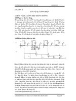
Ideal characteristic
Bias conditions
Forward bias : vd > 0 — current can flow and id > 0.
Reverse bias : vd < 0 — current cannot flow and id = 0.
id
id
Ideal diode
with finite forward drop
(more realistic)
vd
Prof. C.K. Tse: Diode circuits
0.7V
vd
3
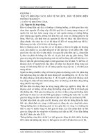
Real characteristic
Take a closer look at the characteristic around the
turning point.
The i-v characteristic is an exponential function.
id
From physics, we have
id = I ss (e q vd
/kT
Also, the diode can only stand the
negative voltage up to a certain
threshold VBD , beyond which
the diode conducts reverse
current (breakdown).
- 1)
–VBD
breakdown
Prof. C.K. Tse: Diode circuits
vd
0.7V
4
Which model to use?
The choice depends on the external voltage magnitudes.
Ideal model:
id = 100/100 = 1 A
With 0.7V drop:
id = (100–0.7)/100
= 0.997 A
Ideal model:
id = 10/100 = 100 mA
With 0.7V drop:
id = (10–0.7)/100
= 93 mA
Prof. C.K. Tse: Diode circuits
Ideal model:
id = 2/100 = 20 mA
With 0.7V drop:
id = (2–0.7)/100
= 13 mA
5
Example: rectifier circuit
The ideal model is valid if the external voltages are well above 0.7V.
What is the magnitude of vr ?
Crude — 50 V
Better — 50 – 1.4 = 48.6 V
Prof. C.K. Tse: Diode circuits
6
Application examples
clamper
dc restorer
half-wave doubler
Prof. C.K. Tse: Diode circuits
full-wave doubler
7
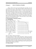
A nonlinear circuit problem
Suppose we wish to find vd , given that the external voltage Vs is not large
enough to validate the use of the ideal diode model.
??
Prof. C.K. Tse: Diode circuits
8
Step 1 : locating the operating points
Recall: The characteristic curve/line for a device actually defines where the point (v, i) can lie.
We know
1
the operating point (vd,
id) is somewhere on the
diode characteristic curve
2
the operating point (vR, iR)
is somewhere on the
resistor characteristic curve
Prof. C.K. Tse: Diode circuits
9
Step 2 : KVL & KCL constraints
We also know
from KCL : id = iR
AND
from KVL : vd + vR = Vs
= Vs
O
+
=
Prof. C.K. Tse: Diode circuits
10
Step 3 : enforcing KVL & KCL
Method:
flip the resistor curve horizontally; and
push the two curves together horizontally until the y-axes are Vs apart.
push
push
add to Vs
Prof. C.K. Tse: Diode circuits
11
Solution : load line
The flipped resistor line is called the LOAD LINE.
Prof. C.K. Tse: Diode circuits
12
General problem
+ vR –
How to find vd and id ?
iR
id
R
:)
Vs
+
_
id
+
vd
–
nonlinear device
vd
Prof. C.K. Tse: Diode circuits
13
Basic load line construction
+ vR –
iR
i
R
:)
Vs
+
_
id
+
vd
–
slope = –1/R
id
device
characteristic
nonlinear device
vd
Prof. C.K. Tse: Diode circuits
v
Vs
14
Alternative construction
+ vR –
iR
i
R
:)
Vs
+
_
id
+
vd
–
id when
device is
short-circuit
nonlinear device
device
characteristic
load line
v
vd when
device is opencircuit
Prof. C.K. Tse: Diode circuits
15
Tutorial problem
Find the operating point.
Prof. C.K. Tse: Diode circuits
16