Thiết kế và lập trình hệ thống - Chương 7
Bạn đang xem bản rút gọn của tài liệu. Xem và tải ngay bản đầy đủ của tài liệu tại đây (284.06 KB, 12 trang )
Systems Design & Programming Memory I CMPE 310
1 (Feb. 25, 2002)
UMBC
U M B C
U
N
I
V
E
R
S
I
T
Y
O
F
M
A
R
Y
L
A
N
D
B
A
L
T
I
M
O
R
E
C
O
U
N
T
Y
1
9
6
6
Memory Types
Two basic types:
• ROM: Read-only memory
• RAM: Read-Write memory
Four commonly used memories:
• ROM
• Flash (EEPROM)
• Static RAM (SRAM)
• Dynamic RAM (DRAM)
Generic pin configuration:
A
0
A
1
A
N
O
0
O
1
O
N
Address connection
Output/Input-output connection
...
...
WE
Write
OE
CS
Read
Select
Systems Design & Programming Memory I CMPE 310
2 (Feb. 25, 2002)
UMBC
U M B C
U
N
I
V
E
R
S
I
T
Y
O
F
M
A
R
Y
L
A
N
D
B
A
L
T
I
M
O
R
E
C
O
U
N
T
Y
1
9
6
6
Memory Chips
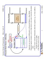
The number of address pins is related to the number of memory locations.
Common sizes today are 1K to 256M locations.
Therefore, between 10 and 28 address pins are present.
The data pins are typically bi-directional in read-write memories.
The number of data pins is related to the size of the memory location.
For example, an 8-bit wide (byte-wide) memory device has 8 data pins.
Catalog listing of 1K X 8 indicate a byte addressable 8K memory.
Each memory device has at least one chip select (
CS) or chip enable (CE) or
select (
S) pin that enables the memory device.
This enables read and/or write operations.
If more than one are present, then all must be 0 in order to perform a
read or write.
Systems Design & Programming Memory I CMPE 310
3 (Feb. 25, 2002)
UMBC
U M B C
U
N
I
V
E
R
S
I
T
Y
O
F
M
A
R
Y
L
A
N
D
B
A
L
T
I
M
O
R
E
C
O
U
N
T
Y
1
9
6
6
Memory Chips
Each memory device has at least one control pin.
For ROMs, an output enable (
OE) or gate (G) is present.
The
OE pin enables and disables a set of tristate buffers.
For RAMs, a read-write (R/
W) or write enable (WE) and read enable (OE)
are present.
For dual control pin devices, it must be hold true that both are not 0
at the same time.
ROM:
Non-volatile memory: Maintains its state when powered down.
There are several forms:
ROM: Factory programmed, cannot be changed. Older style.
PROM: Programmable Read-Only Memory.
Field programmable but only once. Older style.
EPROM: Erasable Programmable Read-Only Memory.
Reprogramming requires up to 20 minutes of high-intensity UV light
exposure.
Systems Design & Programming Memory I CMPE 310
4 (Feb. 25, 2002)
UMBC
U M B C
U
N
I
V
E
R
S
I
T
Y
O
F
M
A
R
Y
L
A
N
D
B
A
L
T
I
M
O
R
E
C
O
U
N
T
Y
1
9
6
6
Memory Chips
ROMs (cont):
Flash EEPROM: Electrically Erasable Programmable ROM.
Also called EAROM (Electrically Alterable ROM) and NOVRAM
(NOn-Volatile RAM).
Writing is much slower than a normal RAM.
Used to store setup information, e.g. video card, on computer sys-
tems.
Can be used to replace EPROM for BIOS memory.
Systems Design & Programming Memory I CMPE 310
5 (Feb. 25, 2002)
UMBC
U M B C
U
N
I
V
E
R
S
I
T
Y
O
F
M
A
R
Y
L
A
N
D
B
A
L
T
I
M
O
R
E
C
O
U
N
T
Y
1
9
6
6
EPROMs
Intel 2716 EPROM (2K X 8):
A
7
V
CC
2K x 8 EPROM
1
2
3
4
5
6
7
8
9
20
19
18
17
16
15
14
13
10
2716
11
12
21
22
23
24
A
6
A
5
A
4
A
3
A
2
A
1
A
0
GND
O
0
O
1
O
2
A
8
A
9
V
PP
CS
A
10
PD/PGM
O
7
O
6
O
5
O
4
O
3
Pin(s)
Function
A
0
-A
10
PD/PGM
CS
O
0
-O
7
Address
Power down/Program
Chip Select
Outputs
Chip Select
PWR Down
Prog Logic
Y
Decoder
X
Decoder
CS
PD/PGM
Address Inputs
Data Outputs
Output
Buffers
Y-Gating
16,384
Cell Matrix
V
PP
is used to program the device
by applying 25V and pulsing PGM
while holding
CS high.