Thiết kế và lập trình hệ thống - Chương 8
Bạn đang xem bản rút gọn của tài liệu. Xem và tải ngay bản đầy đủ của tài liệu tại đây (574.13 KB, 21 trang )
Systems Programming 8086/88 Memory Interface II CMPE 310
1 (April 10, 2000 12:36 pm)
UMBC
U M B C
U
N
I
V
E
R
S
I
T
Y
O
F
M
A
R
Y
L
A
N
D
B
A
L
T
I
M
O
R
E
C
O
U
N
T
Y
1
9
6
6
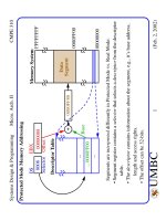
Memory Address Decoding
The processor can usually address a memory space that is much larger than
the memory space covered by an individual memory chip.
In order to splice a memory device into the address space of the processor,
decoding is necessary.
For example, the 8088 issues 20-bit addresses for a total of 1MB of memory
address space.
However, the BIOS on a 2716 EPROM has only 2KB of memory and 11
address pins.
A decoder can be used to decode the additional 9 address pins and allow the
EPROM to be placed in any 2KB section of the 1MB address space.
Systems Programming 8086/88 Memory Interface II CMPE 310
2 (April 10, 2000 12:36 pm)
UMBC
U M B C
U
N
I
V
E
R
S
I
T
Y
O
F
M
A
R
Y
L
A
N
D
B
A
L
T
I
M
O
R
E
C
O
U
N
T
Y
1
9
6
6
Memory Address Decoding
A
0
A
1
A
10
O
0
O
1
O
7
...
...
CS
RD of 8088/86
2716
IO/M
A
19
A
18
A
17
A
16
A
15
A
14
A
13
A
12
A
11
Address Bus Data Bus
Logic 0 when A
11
through A
19
are all 1.
Or MRDC bus signal.
(2K X 8)
(Book shows
OE
connection
for RD
but
chip definition
does NOT have
EPROM
this pin).
Systems Programming 8086/88 Memory Interface II CMPE 310
3 (April 10, 2000 12:36 pm)
UMBC
U M B C
U
N
I
V
E
R
S
I
T
Y
O
F
M
A
R
Y
L
A
N
D
B
A
L
T
I
M
O
R
E
C
O
U
N
T
Y
1
9
6
6
Memory Address Decoding
To determine the address range that a device is mapped into:
This 2KB memory segment maps into the reset location of the 8086/8088
(FFFF0H).
NAND gate decoders are not often used.
Rather the 3-to-8 Line Decoder (74LS138) is more common.
1111 1111 1XXX XXXX XXXX
A
19
- A
11
A
10
- A
0
1111 1111 1000 0000 0000 (FF800H)
To
1111 1111 1111 1111 1111 (FFFFFH)
Systems Programming 8086/88 Memory Interface II CMPE 310
4 (April 10, 2000 12:36 pm)
UMBC
U M B C
U
N
I
V
E
R
S
I
T
Y
O
F
M
A
R
Y
L
A
N
D
B
A
L
T
I
M
O
R
E
C
O
U
N
T
Y
1
9
6
6
Memory Address Decoding
The 3-to-8 Line Decoder (74LS138)
Note that all three Enables (G2A, G2B, and G1) must be active, e.g. low, low
and high, respectively.
Each output of the decoder can be attached to an 2764 EPROM (8K X 8).
G2A
G2B
G1
A
B
C
0
1
2
3
4
5
6
7
Enable
Select Inputs
Outputs
Inputs
Output
Enable Select
G2A G2B G1
C B A 0 1 2 3 4 5 6 7
1 X X X X X 1 1 1 1 1 1 1 1
X 1 X X X X 1 1 1 1 1 1 1 1
X X 0 X X X 1 1 1 1 1 1 1 1
0 0 1 0 0 0 0 1 1 1 1 1 1 1
0 0 1 0 0 1 1 0 1 1 1 1 1 1
0 0 1 0 1 0 1 1 0 1 1 1 1 1
0 0 1 0 1 1 1 1 1 0 1 1 1 1
0 0 1 1 0 0 1 1 1 1 0 1 1 1
0 0 1 1 0 1 1 1 1 1 1 0 1 1
0 0 1 1 1 0 1 1 1 1 1 1 0 1
0 0 1 1 1 1 1 1 1 1 1 1 1 0
Systems Programming 8086/88 Memory Interface II CMPE 310
5 (April 10, 2000 12:36 pm)
UMBC
U M B C
U
N
I
V
E
R
S
I
T
Y
O
F
M
A
R
Y
L
A
N
D
B
A
L
T
I
M
O
R
E
C
O
U
N
T
Y
1
9
6
6
Memory Address Decoding
The EPROMs cover a 64KB section of memory.
G2A
G2B
G1
A
B
C
0
1
2
3
4
5
6
7
A
0
A
12
O
0
O
7
... ...
CS
2764
A
16
A
17
A
18
A
19
A
13
A
14
A
15
CS
CS
CS
CS
CS
CS
CS
RD of 8088/86
Data Bus
Address Bus
F2000-F3FFF
F0000-F1FFF
F4000-F5FFF
F6000-F7FFF
F8000-F9FFF
FA000-FBFFF
FC000-FDFFF
FE000-FFFFF
Address space
F0000H-FFFFFH
A
13
through A
15
select
a 2764
A
16
through A
19
enable
the decoder
(8K X 8)
(Not sure about 2764 pinout,
text is in error with 2716)
74LS138
EPROM
Systems Programming 8086/88 Memory Interface II CMPE 310
6 (April 10, 2000 12:36 pm)
UMBC
U M B C
U
N
I
V
E
R
S
I
T
Y
O
F
M
A
R
Y
L
A
N
D
B
A
L
T
I
M
O
R
E
C
O
U
N
T
Y
1
9
6
6
Memory Address Decoding
Yet a third possibility is a PLD (Programmable Logic Device).
PLDs come in three varieties:
• PLA (Programmable Logic Array)
• PAL (Programmable Array Logic)
• GAL (Gated Array Logic)
PLDs have been around since the mid-1970s but have only recently appeared
in memory systems (PALs have replaced PROM address decoders).
PALs and PLAs are fuse-programmed (like the PROM).
Some are erasable (like the EPROM).
A PAL example (16L8) is shown in the text and is commonly used to decode
the memory address, particularly for 32-bit addresses generated by the
80386DX and above.
Systems Programming 8086/88 Memory Interface II CMPE 310
7 (April 10, 2000 12:36 pm)
UMBC
U M B C
U
N
I
V
E
R
S
I
T
Y
O
F
M
A
R
Y
L
A
N
D
B
A
L
T
I
M
O
R
E
C
O
U
N
T
Y
1
9
6
6
Memory Address Decoding
AMD 16L8 PAL decoder.
It has 10 fixed inputs (Pins 1-9, 11), two fixed outputs (Pins 12 and 19)
and 6 pins that can be either (Pins 13-18).
AND/NOR device with logic expressions (outputs) with up to 16
ANDed inputs and 7 ORed product terms.
O3
1
2
3
4
5
6
7
15
11
20
19
16
16L8
17
18
I4
I5
I6
I7
V
CC
I3
I2
O6
O8
I1
O4
O5
O7
9
8
10
12
13
14
I8
I9
GND
O2
O1
I10
;pins 1 2 3 4 5 6 7 8 9 10
A19
A18 A17 A16 A15 A14 A13 NC NC GND
;pins 11 12 13 14 15 16 17 18 19 20
NC O8 O7 O6 O5 O4 O3 O2 O1 VCC
Equations:
/O1 = A19 * A18 * A17 * A16 * /A15 * /A14 * /A13
/O2 = A19 * A18 * A17 * A16 * /A15 * /A14 * A13
/O3 = A19 * A18 * A17 * A16 * /A15 * A14 * /A13
/O4 = A19 * A18 * A17 * A16 * /A15 * A14 * A13
/O5 = A19 * A18 * A17 * A16 * A15 * /A14 * /A13
/O6 = A19 * A18 * A17 * A16 * A15 * /A14 * A13
/O7 = A19 * A18 * A17 * A16 * A15 * A14 * /A13
/O8 = A19 * A18 * A17 * A16 * A15 * A14 * A13
Programmed to decode address lines A
19
- A
13
onto 8 outputs.
Systems Programming 8086/88 Memory Interface II CMPE 310
8 (April 10, 2000 12:36 pm)
UMBC
U M B C
U
N
I
V
E
R
S
I
T
Y
O
F
M
A
R
Y
L
A
N
D
B
A
L
T
I
M
O
R
E
C
O
U
N
T
Y
1
9
6
6
8088 and 80188 (8-bit) Memory Interface
The memory systems “sees” the 8088 as a device with:
• 20 address connections (A19 to A0).
• 8 data bus connections (AD7 to AD0).
• 3 control signals, IO/M, RD, and WR.
We’ll look at interfacing the 8088 with:
• 32K of EPROM (at addresses F8000H through FFFFFH).
• 512K of SRAM (at addresses 00000H through 7FFFFH).
The EPROM interface uses a 74LS138 (3-to-8 line decoder) plus 8 2732 (4K X
8) EPROMs.
The EPROM will also require the generation of a wait state.
The EPROM has an access time of 450ns.
The 74LS138 requires 12ns to decode.
The 8088 runs at 5MHz and only allows 460ns for memory to access data.
A wait state adds 200ns of additional time.