Thiết kế và lập trình hệ thống - Chương10
Bạn đang xem bản rút gọn của tài liệu. Xem và tải ngay bản đầy đủ của tài liệu tại đây (291.43 KB, 15 trang )
Systems Design and Programming Basic I/O II CMPE 310
1 (Apr. 10, 2002)
UMBC
U M B C
U
N
I
V
E
R
S
I
T
Y
O
F
M
A
R
Y
L
A
N
D
B
A
L
T
I
M
O
R
E
C
O
U
N
T
Y
1
9
6
6
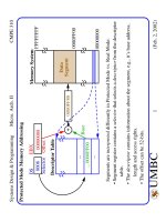
Programmable Peripheral Interface (82C55)
The 82C55 is a popular interfacing component, that can interface any TTL-
compatible I/O device to the microprocessor.
It is used to interface to the keyboard and a parallel printer port in PCs (usu-
ally as part of an integrated chipset).
Requires insertion of wait states if used with a microprocessor using higher
that an 8 MHz clock.
PPI has 24 pins for I/O that are programmable in groups of 12 pins and has
three distinct modes of operation.
In the PC, an 82C55 or its equivalent is decoded at I/O ports 60H-63H.
Systems Design and Programming Basic I/O II CMPE 310
2 (Apr. 10, 2002)
UMBC
U M B C
U
N
I
V
E
R
S
I
T
Y
O
F
M
A
R
Y
L
A
N
D
B
A
L
T
I
M
O
R
E
C
O
U
N
T
Y
1
9
6
6
Pinout of 82C55 PPI
D1
D2
D3
D4
D5
D6
D7
D0
82C55
RD
WR
A0
A1
CS
RESET
VCC
GND
A
1
A
0
Function
0
0
1
1
0
1
0
1
I/O Port Assignments
Port A (PA7-PA0) and upper
half of port C (PC7 - PC4)
Group A
Port B (PB7-PB0) and lower
half of port C (PC3 - PC0)
Group B
Port A
Port B
Port C
Command Register
PA1
PA2
PA3
PA4
PA5
PA6
PA7
PA0
PB1
PB2
PB3
PB4
PB5
PB6
PB7
PB0
PC1
PC2
PC3
PC4
PC5
PC6
PC7
PC0
Systems Design and Programming Basic I/O II CMPE 310
3 (Apr. 10, 2002)
UMBC
U M B C
U
N
I
V
E
R
S
I
T
Y
O
F
M
A
R
Y
L
A
N
D
B
A
L
T
I
M
O
R
E
C
O
U
N
T
Y
1
9
6
6
Interfacing the 82C55 PPI
Port A
Port B
Port C
A7
A3
A4
A6
A5
A0
A
B
C
G1
G2A
G2B
0
1
2
3
4
5
6
7
74ALS138
IORC
IOWC
A1
A2
RESET
D1
D2
D3
D4
D5
D6
D7
D0
PA1
PA2
PA3
PA4
PA5
PA6
PA7
PA0
PB1
PB2
PB3
PB4
PB5
PB6
PB7
PB0
PC1
PC2
PC3
PC4
PC5
PC6
PC7
PC0
RD
WR
A0
A1
CS
RESET
VCC
GND
82C55
(C0H)
(C2H)
(C4H)
(C6H)
Command
Register
(Port addresses)
D
7
--D
0
8
Systems Design and Programming Basic I/O II CMPE 310
4 (Apr. 10, 2002)
UMBC
U M B C
U
N
I
V
E
R
S
I
T
Y
O
F
M
A
R
Y
L
A
N
D
B
A
L
T
I
M
O
R
E
C
O
U
N
T
Y
1
9
6
6
Programming the 82C55
Port C (PC3 - PC0)
1 = input
0 = output
Port B
1 = input
0 = output
Mode
0 = mode 0
1 = mode 1
Mode
00 = mode 0
01 = mode 1
1x = mode2
Port A
1 = input
0 = output
Port C (PC7 - PC4)
1 = input
0 output
1
7
Command Byte A
Command Byte B
Bit set/reset
1 = set
0 = reset
Selects a bit
(Programs ports A, B, C)
0
Group B
Group A
(Sets or resets any bits in port C)
6 5 4 3 2 1 0
x x x
7 6 5 4 3 2 1 0
Systems Design and Programming Basic I/O II CMPE 310
5 (Apr. 10, 2002)
UMBC
U M B C
U
N
I
V
E
R
S
I
T
Y
O
F
M
A
R
Y
L
A
N
D
B
A
L
T
I
M
O
R
E
C
O
U
N
T
Y
1
9
6
6
82C55: Mode 0 Operation
D
7
--D
0
82C55
D
0
D
7
A
0
A
7
B
7
B
0
C
7
C
0
A
0
A
1
Reset
IORC
IOWC
7
7
8-Digit Seven Segment LED Display Interface
NC
Vcc
Gnd
16L8
A
4
A
5
A
6
A
8
A
9
A
7
A
10
A
12
A
14
A
15
A
13
IO/M
A
11
CS
A
0
A
1
RD
WR
Reset
I
1
I
10
O
1
O
8
A
3
A
2
8
Systems Design and Programming Basic I/O II CMPE 310
6 (Apr. 10, 2002)
UMBC
U M B C
U
N
I
V
E
R
S
I
T
Y
O
F
M
A
R
Y
L
A
N
D
B
A
L
T
I
M
O
R
E
C
O
U
N
T
Y
1
9
6
6
82C55: Mode 0 Operation
Mode 0 operation causes the 82C55 to function as a buffered input device or
as a latched output device.
In previous example, both ports A and B are programmed as (mode 0) simple
latched output ports.
Port A provides the segment data inputs to display and port B provides a
means of selecting one display position at a time.
Different values are displayed in each digit via fast time multiplexing.
The values for the resistors and the type of transistors used are determined
using the current requirements (see text for details).
Textbook has the assembly code fragment demonstrating its use.
Examples of connecting LCD displays and stepper motors are also given.