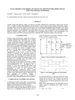
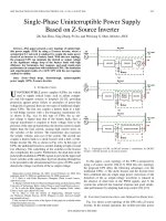
Z source inverter for UPS application
Bạn đang xem bản rút gọn của tài liệu. Xem và tải ngay bản đầy đủ của tài liệu tại đây (859.99 KB, 5 trang )
1-4244-1355-9/07/$25.00 @2007 IEEE
International Conference on Intelligent and Advanced Systems 2007
~ 835
Z-Source Inverter for UPS Application
R.Senthilkumar, R.Bharanikumar, Jovitha Jerom
Bannari Amman Institute of Technology PSG College of Technology
Sathyamangalam, Coimbatore
Tamil Nadu, India
Abstract- This project proposes an impedance-source inverter and its
control method for implementing dc-to-ac, ac-to-dc, ac-to-ac, and dc-to-dc
power conversion. The Z-source converter employs a unique impedance
network to couple the converter main circuit to the power source. The Z-
source converter overcomes the conceptual and theoretical barriers and
limitations of the traditional voltage-source converter and current-source
converter and provides a novel power conversion concept. The Z-source
concept can be applied to all dc-to-ac, ac-to-dc, ac-to-ac, and dc-to-dc power
conversion. To describe the operating principle and control, this paper
focuses on an Uninterrupted Power Supply (UPS) applications
Keywords- ZSI, VSI, CSI, Inverter
I.
I
NTRODUCTION
raditionally there are two inverters available.
These are voltage source inverters and current source
inverters. Each inverter has two switches in the main circuit.
These switches are power switches with anti-parallel diodes.
These diodes provide bidirectional current flow and reverse
voltage blocking capability. Traditional inverters have following
limitations .They can operate either as a boost or buck inverter
and cannot be a buck-boost inverter. Their output voltage range
is limited to either greater or smaller than the input voltage.
Their main circuit is not being interchangeable. In other words
neither the voltage source inverter can be used for the current
source inverter nor vice versa. They are vulnerable to EMI noise
in terms of reliability. The above limitations can be rectified in
impedance source inverter to get higher efficiency. This concept
can be applied to all AC to DC, AC to AC, DC to DC, DC to AC
power conversions [4].
II. TRADITIONAL SOURCE INVERTERS
Traditional source inverters are voltage source inverters and
current inverters. The output of voltage source inverter is a stiff
dc voltage supply, which can be a battery or a controlled
R.Senthilkumar Asst.Professor EEE Department Bannari Amman Institute of
technology Sathyamangalam.e-mail id:
R.Bharanikumar Asst.Professor EEE DepartmentBannari Amman Institute of
technology Sathyamangalam.e-mail id:
Dr.Jovitha Jerome Professor, C&I Department, PSG college of Technology,
Coimbatore.e-mail id:
rectifier (both single phase and single phase voltage source
inverter). The switching device can be a conventional MOSFET,
thyristor or a power transistor.
A. Traditional source inverters
Traditional source inverters are voltage source inverters and
current inverters. The output of voltage source inverter is a stiff
dc voltage supply, which can be a battery or a controlled rectifier
(both single phase and single phase voltage source inverter). The
switching device can be a conventional MOSFET, thyristor or a
power transistor. Voltage source inverter is one in which the dc
source has small or negligible impedance. In other words a
voltage source has stiff dc source voltage at its input terminals.
A current source- fed inverter or current source inverter is fed
with adjustable dc current source. In current source inverter,
output current waves are not affected by the load.
B. Voltage source inverter [VSI]
The traditional voltage-source inverter input is a dc voltage
source supported by a relatively large voltage source can be a
battery, fuel-cell stack, diode rectifier, and/or capacitor. Four
switches are used in the main circuit; each in traditionally
bidirectional current flow and unidirectional voltage blocking
capability. The V-source inverter is widely used however; it has
the following conceptual limitations [5].
C. Limitations of voltage source inverter
The V-source inverter is buck (step down) inverter for dc-to-
ac power conversion. For applications where over drive is
desirable and the available dc voltage is limited, an additional
dc-dc boost (step up) stage is needed to obtain a desired ac
output [1]. The additional power converter stage increases
system cost and lowers efficiency.
The upper and lower devices of each phase leg cannot be
gated on simultaneously either by purpose or by EMI noise.
Otherwise, a shoot-through would occur and destroy the devices.
The shoot-through problem by electromagnetic interference
(EMI) noise’s misgating-on is a major killer to the inverter to the
inverter’s reliability. Dead time to block both upper and lower
devices has to be provided in the V-source inverter, which
causes waveform distortion, etc. [1]. An output LC filter is
needed for providing a sinusoidal voltage compared with the
current-source inverter, which causes additional power loss and
control complexity.
D. Current source inverter
[CSI]
The traditional current-source inverter input is a dc current
source feeds by the main converter circuit. The dc current source
can be a relatively large dc inductor fed by a voltage source such
as a battery, fuel-cell stack, diode rectifier, or thyristor
converter. Four switches are used in the main circuit; each is
traditionally composed of a semiconductor switches device with
reverse block capacity such as gate-turn-off thyristor (GTO) and
SCR or a power transistor with a series diode to provide
unidirectional current flow and bidirectional voltage blocking.
However, the current -source inverter has the following
conceptual barriers and limitations. [2]
T
-20 -18 -16 -14 -12 -10 -8 -6 -4 -2 0 2
0
5
10
15
20
25
exciter mode
inter area
mode
Figure 6. Root locus with PSS, Alternative-I
TABLE 6
D
OMINANT
P
OLES WITH
PSS
AT
M
ACHINE
3
AND
4,
ALTERNATIVE-I
Initial Estimate Dominant Poles Damping Ratio
0 + 3.0000i -0.2627 + 3.0542i 0.0857
0 - 3.0000i -0.2627 - 3.0542i 0.0857
TABLE 7
WITHOUT PSS, ALTERNATIVE-II
Estimate
Dominant
eigenvalue
Damping Ratio
Frequency of
oscillation
0 + 3.0000i 0.0211 + 3.2250i -0.0065 0. 513
0 - 3.0000i 0.0211 -3.2250i -0.0065 0. 513
Table7 exhibits dominant poles of the system in Alternative-
II. Again the inter-area modes are unstable with negative
damping.
Corresponding root locus is shown in figure 7. The PSS
designed for Alternative-I when used in this configuration,
damping improves to 2.81% as shown in Table 8. The
corresponding root locus shown in figure 8 indicates an
additional stable mode with a preferred damping of 5 %.
-20 -18 -16 -14 -12 -10 -8 -6 -4 -2 0 2
0
2
4
6
8
10
12
14
16
18
20
inter
area
modes
exciter modes
Figure 7 Root locus, without PSS, Alternative-II
TABLE8
DOMINANT POLES WITH PSS, ALTERNATIVE-II
Initial Estimate Dominant Eigen values Damping Ratio
0 + 3.0000i -0.0896 + 3.1888i 0.0281
0 - 3.0000i -0.0896 - 3.1888i 0.0281
-25 -20 -15 -10 -5 0
0
5
10
15
20
25
inter
area
mode
exciter
modes
Figure 8 Root locus with PSS, Alternative-II
C
ONCLUSIONS
Only a few of the numerous modes of oscillation in a large
interconnected power system are of interest for control design.
Multivariable state space description overcomes hidden
dynamics or uncontrollable/unobservable modes related
difficulties. Modal approximation of the transfer function
matrix using dominant poles enables control design for
suppressing inter-area oscillations, while reducing
computation volume.
R
EFERENCES
[1] Graham Rogers.
Power System Oscillations
. Kluwer Academic b
Publishers, Boston, 2000.
[2] R. Sadikovic, “Damping Controller Design for Power System
Oscillations”, Internal Report, Zurich, 2004.
[3] M. Klein, G.J. Rogers, and P. Kundur. “A fundamental study of inter-
area oscillations in power systems,”
IEEE Trans. on power systems
, vol.
6(3), 1991.
[4] J. Machowski, J. W. Bialek, J. R. Bumby,
Power system Dynamics and
Stability.
John Wiley & Sons.
[5] Tan Kar Khai, R.N.Mukerjee
, “
Investigations into interplay mechanism
between inter-area and local oscillatory modes in a power system
”,
7
th
IEE international Conference on Advances in Power System Control,
Operation and Management, Hong Kong, Paper Reference Number:
APSCOM 2006-157, 30
th
Oct 2
nd
November, 2006.
[6] N.M. Muhamad Razali, R. N. Mukerjee, V. K. Ramachandaramurthy,
“
Integrated Modelling and Residue Method Based Tuning of PWM
based STATCOM for Suppressing Power System Oscillations
“
,
proceedings, pp 110-114, The 8
th
IEE International conference on AC
and DC Power Transmission, ACDC 2006, 28-31 March 2006, Savoy
Place, London
[7] J M. Macieejowski,
Multivariable feedback design,
Addison-Wesley
[8] Nelson Martins, Paulo E. M. Quintão, “Computing Dominant Poles of
Power System Multivariable Transfer Functions”
IEEE Transaction
on Power Systems
, Vol. 18, No. 1, 2003.
[9] IEEE Std. Recommended Practice for Excitation System Models for
Power System Stability Studies, 1992.
International Conference on Intelligent and Advanced Systems 2007
836 ~
E. Limitations of current source inverter
The ac output voltage has to be greater than the original dc
voltage that feeds the dc inductor or the dc voltage produced is
always smaller than the ac input voltage. For applications where
a wide voltage range is desirable, an additional dc-dc boost stage
is needed. The additional power conversion stage increases
system cost and lowers efficiency. [1]At least one of the upper
devices and one of the lower devices have to be gated on and
maintained on at any time. Otherwise, an open circuit of the dc
inductor would occur and destroy the devices. The open-circuit
problem by EMI noise’s misgating-off is a major concern of the
converter’s reliability [3].overlap time for safe current
commutation is needed in the I-source converter, which also
causes waveform distortion. The main switches of the I-source
inverter have to block reverse voltage that requires a series diode
to be used in combination with high-speed and high-
performance transistors such as insulated gate bipolar transistors
(IGBT). This prevents the direct use of low-cost and high-
performance IGBT modules.
F. Limitations in both voltage and current source inverter
Their obtained output voltage range is limited to either
greater or smaller than the input voltage [2]. Their main circuit
cannot be interchangeable. In other words, neither the V-source
inverter main circuit can be used for the I-source inverter nor
vice versa. They are vulnerable to EMI noise in terms of
reliability [5].
III
IMPEDANCE SOURCE INVERTER
A. Block diagram of impedance source inverter
To overcome the above limitations of the traditional V-source
and I-source inverter, this thesis deals an impedance-source
inverter and its control method for impedance dc-to-ac power
conversion. This thesis also deals with how to overcome the
limitations of voltage source inverter and current source inverter
Single
Pha s e
AC
Sup ply
Rect ifier
Unit
Impedan ce
Network
Inverter L
oad
Figure 1. Block diagram of Impedance Source Inverter
TABLE 1
Comparison of VSI, CSI and ZSI
Current Source
Inverter (CSI)
Voltage Source
Inverter(VSI)
Impedance
Source Inverters (ZSI)
1. As inductor is used
in the d.c link, the
source Impedance is
high. It acts as a
constant current
source.
2. A current source
inverter is capable of
withstanding short
circuit across any two
of its output terminals.
Hence momentary
short circuit on load
and mis-firing of
switches are
acceptable.
3. This is used in only
buck or boost
operation of inverter.
4. The main circuits
cannot b
e
interchangeable.
5. It is affected by the
EMI noise.
6. It has a considerable
amount of harmonic
distortion
7. Power loss should
be high because of
filter
8. Lower efficiency
because
of high power loss
As capacitor is used
in the d.c link, it acts
as a low impedance
voltage source.
A VSI is more
dangerous situation
as the parallel
Capacitor feeds more
powering to the fault.
This is also used in a
buck or boost
operation of inverter.
The main circuit
cannot be
Interchange
able here also.
It is affected by the
EMI noise
It has a considerable
amount of harmonic
distortion
Power loss is high
Efficiency should be
low because of high
power
loss
As capacitor and inductor
is used in the d.c link, it
acts
as a constant high
impedance voltage
source.
In ZSI mis-firing of the
switches are also
acceptable sometimes.
This is used in both buck
and boost operation of
Inverter.
Here the main circuits are
Interchange
able
It is less affected by the
EMI noise.
Harmonics Distortion is
low
Power loss should
be low
Higher efficiency
because of less
power loss
The proposed impedance source inverter block diagram is
shown in Fig 1. It is consists of rectifier unit, Impedance
network, single phase inverter and load. AC voltage is rectified
to DC voltage by the rectifier. The rectified output DC voltage is
fed to the network
B. Advantages of the impedance source network
The impedance source inverter concept can be applied in all
ac-ac, dc-dc, ac-dc, dc-ac power conversion. The output voltage
range is not limited. The impedance source inverter is used as a
buck-boost inverter. The impedance source inverter does not
affect the electro magnetic interference noise. The impedance
source inverter cost is low. The impedance source inverter
International Conference on Intelligent and Advanced Systems 2007
~ 837
provides the buck-boost function by two stage power
conversion.
IV ANALYSIS AND DESIGN OF THE IMPEDANCE
NETWORK
A. Equivalent circuit, operating principle, and control
The unique feature of the impedance-source inverter is that
the output ac voltage can be any value between zeros to infinity
regardless of the DC voltage. That is, the impedance-source
inverter is a buck-boost inverter that has a wide range of
obtainable voltage. The traditional V-and I-source inverters
cannot provide such feature. To describe the operating principle
and control of the impedance-source inverter in Fig. 2, let us
briefly examine the impedance-source inverter structure.
C 2
L2
C1
L1
DC
D2
+ +
+ +
+
+
-
-
-
Vd Vi i1
Figure 2. Equivalent Circuit of Impedance Source Inverter
The single -phase Z-source Inverter Bridge has six
permissible switching states unlike the traditional single-phase
V-source inverter that has five. The traditional single-phase V-
source inverter has five active vectors when the dc voltage is
impressed across the load and one zero vector when the load
terminals are shorted through either the lower or upper single
devices, respectively. However, the single-phase impedance-
source inverter bridge has one extra zero state.
When the load terminals are shoot-through both the upper and
lower devices of any one phase leg. This shoot-through zero
state is forbidden in the traditional V-source inverter, because it
would cause a shoot-through. We call this third zero state the
shoot-through zero state, which can be generated by seven
different ways: shoot-through via any one phase leg,
combinations of any two phase legs, and all single phase legs.
The impedance source network makes the shoot-through zero
state possible.
Figure 3. Equivalent circuit of the impedance source inverter viewed form the
dc link
The inverter bridge is equivalent to a short circuit when the
inverter bridge is in the shoot-through zero state, as shown in
Fig.3, whereas the inverter bridge becomes an equivalent current
source as shown in Fig 3 when in one of the six active states.
The inverter bridge can be also represented by a current
source with zero value (i.e., an open circuit) when it is in one of
the two traditional zero states. Therefore, Fig. 3, shows the
equivalent circuit of the Z-source inverter viewed from the dc
link when the inverter bridge is in one of the eight nonshoots-
through switching states. All the traditional pulse width-
modulation (PWM) schemes can be used to control the Z-source
inverter and their theoretical input–output relationships still hold
[1].
V CIRCUIT ANALYSIS AND OBTAINABLE OUTPUT
VOLTAGE
From the symmetry and the equivalent circuits, we have
V
C1
=V
C2
=V
C
; V
L1
=V
L2
=V
L
(1)
Given that the inverter bridge is in the shoot-through zero state
for an interval ofT0, during a switching cycle, T and from the
equivalent circuit, Fig. 3 one has
V
L
=V
C
; V
d
=2V
C
; V
i
=0 (2)
Now consider that the inverter bridge is in one of the eight
nonshoots- through states for an interval of T, during the
switching cycle, from the equivalent circuit,
V
l
=V
0
-V
C
: V
d
=V
0
; Vi=V
C
=V
L
=2V
C
-V
0
(3)
Where V
O
is the dc source voltage and T=T
0
+T
1
.
The average voltage of the inductors over one
switching period (T) should be zero in steady state, from
equation (2) and equation (3), we have
V
L
=V
l
=T
0
.V
C
+ (T
1
(V
0
- V
C
))/T = 0 (4)
V
C
/V
0
=T
1
/(T
1
-T
0
) (5)
Similarly, the average dc-link voltage across the inverter bridge
can be found as follows:
V
l
=V
i1
=T
0
+T
1
(2V
C
-V
0
))/T=
(T
1
/ (T
1
-T
0
)) V
0
=V
C
(6)
For the traditional V-source PWM inverter, we have the well
known relationship
:
V
S
=M.BV
0
/2 (7)
Equation shows that the output voltage can be stepped up and
down by choosing an appropriate buck-boost factor,
Bb=M*B (0 to Į) (8)
From (1),(6) and (7), the capacitor voltage can expressed as
V
C
1=V
C
2= ((1-(T
0
/T))/ (1-2(T
0
/T)) V
0
(9)
International Conference on Intelligent and Advanced Systems 2007
838 ~
The buck–boost factor is determined by the modulation index
and boost factor. The boost factor can be controlled by duty
cycle (i.e., interval ratio) of the shoot-through zero state over the
nonshoots-through states of the inverter PWM. Note that the
shoot-through zero state does not affect the PWM control of the
inverter, because it equivalently produces the same zero voltage
to the load terminal.
The available shoot through period is limited by the zero-state
period that is determined by the modulation index. The
impedance source network should require less capacitance and
smaller size compared with the traditional V-source inverter.
Similarly, when the two capacitors are small and approach zero
the impedance source network reduces to two inductors in series
and becomes a traditional I-source. Therefore, a traditional I-
source inverter’s inductor requirements and physical size is the
worst case requirement for the impedance source network.
Considering additional filtering and energy storage by the
capacitors, the impedance source network should require less
inductance and smaller size compared with the traditional I-
source inverter [1].
VI.
SIMULATION CIRCUIT AND RESULTS OF THE
IMPEDANCE SOURCE INVERTER
Simulations have been performed to confirm the above
analysis. Fig shows the main circuit configuration of impedance
source inverter for UPS application. The impedance network
parameters are L1=L2=160µH and C1=C2=C=1000µF. The
purpose of the system is to produce single phase 208V rms
power from the DC source whose voltage changes 150-240V dc
depending on load current.
0
L1
160u
C2
100u
C1
100u
D4
SD51
D3
SD51
D2
SD51
D1
SD51
M4
IR FP450
M3
IR FP450
M2
IRF P450
M1
IRF P450
L2
160u
V4V3
V2
V1
R1
5k
V5
Figure 4. Circuit Diagrams of impedance source inverter
Figure. 5, shows the input voltage and output voltage of the
z-source inverter. Input voltage is 100V AC supply. The output
voltage 100V DC is given by the rectifier unit. The output
voltage of impedance source inverter is shown above.
Figure 5. Input and Output voltage waveform
The simulation proved the impedance source inverter concept.
The waveforms are consistent with the simulation results.
Figure 6. Modified gating pulse
VII.
EXPERIMENTAL RESULTS
The z-source inverter is practically implemented and the
hardware results obtained satisfy the specifications.
The Figure. 7, shows the PWM pulses with a phase shift of
180
0
each other and is applied to the MOSFETs of single
phase inverter. Here there is no delay time between the pulses
but there is a shoot through in between the pluses. The pulses
are generated at a voltage of magnitude 14 volts
Figure 7. Pulses before the Driver Circuit
International Conference on Intelligent and Advanced Systems 2007
~ 839
The voltage waveform is obtained after the impedance
source terminals. This is a sine waveform which is fed to the
inverter. There is no need of output filter. Impedance source acts
as a second order filter
.
Figure 8. Input of Inverter Circuit (Z-Source Output Voltage)
This is a sine output voltage waveform of the inverter
circuit across the load terminals and has the amplitude of
30Volts and frequency of 50Hz
Figure 9. Output Voltages across the Load
Variable inputs and load conditions are tabulated below. The
input AC voltage ranges from 100V to 160V and the load to be
fed to the switching equipment also varies correspondingly. For
any such variation in the input side as well as the load, the
output AC voltage changes according to the input voltage.
Finally a pure constant AC voltage is obtained and it is fed to
the switching equipment of the UPS. This voltage is utilized to
track the route to provide efficient UPS Application. Hardware
results also ensure it.
VIII.
CONCLUSION
A new type of inverter for UPS application has been proposed
and corresponding simulated waveforms are verified. The
Impedance source inverter is specially suited for above
applications. Unique features like single stage power conversion,
improved reliability, strong EMI immunity and low EMI. The
impedance source technology can be applied to the entire
spectrum of power conversion.
REFERENCES
[1] F. Z. Peng, “Z-Source inverter,” IEEE Trans. Ind Applicat., vol. 39, pp.504–
510, Mar. /Apr. 2003.
[2] F. Z. Peng, X. Yuan, X. Fang, and Z. Qian, “Z-source inverter for adjustable
speed drives,” IEEE Power Electron. Lett., vol. 1, no. 2, pp. 33–35, Jun.
2003.
[3] F. Z. Peng, M. Shen, and Z. Qian, “Maximum boost control of the z-source
inverter,” in Proc. 39th IEEE Industry Applications Conf., vol. 1, Oct. 2004.
[4] M. Shen, J.Wang, A. Joseph, F. Z. Peng, L. M. Tolbert, and D. J. Adams,
“Maximum constant boost control of the Z-source inverter,” presented at the
IEEE Industry Applications Soc. Annu. Meeting, 2004.
[5] Theory on single phase inverters are presented by M.H.RASHID in power
electronics circuit device and applications, 2nd edition, Englewood cliffs,
N.J.,prentice-hall, 1993.
[6] Design of the impedance network is presented by COMPTUN.K.T in
electrics handbook, 6th edition, London, 1947.
BIOGRAPHY
Senthil Kumar.R was born in Tamilnadu, India, on
November 2, 1966. He received the B.E degree in Electrical
and Electronics Engineering from Madurai Kamaraj
University, in 1989. He received his M.E (Power systems)
from Annamalai University, in 1991. He has 15 yrs of
teaching experience. Currently he is working as Asst.
Professor in EEE department, Bannari Amman Institute of
Technology, Sathyamanglam. Currently he is doing research
in the field of power converters for UPS Applications.
Bharanikumar R. was born in Tamilnadu,
India, on may 30, 1977. He received the B.E degree in
Electrical and Electronics Engineering from Bharathiyar
University, in 1998. He received his M.E Power Electronics
and Drives from college of Engineering Guindy Anna
University in 2002.He has 8 yrs of teaching experience.
Currently he is working as Asst. Professor in EEE
department, Bannari Amman Institute of Technology,
Sathyamanglam. Currently he is doing research in the field of
power converter for special machines; vector controlled based
synchronous machine drives, converters for wind energy
conversion systems.
Dr. Jovitha Jerome was born in Tamilnadu, India, on June
2, 1957. She received the B.E. degree in Electrical and
Electronics Engineering and M.E. degree in Power Systems
from College of Engineering, Guindy, Chennai. She did her
DEng in Power Systems. Presently she is working as
Professor and Head in Instrumentation and Control
Engineering Department of PSG College of Technology,
Coimbatore