Bài tập cảm biến và kỹ thuật đo lường
Bạn đang xem bản rút gọn của tài liệu. Xem và tải ngay bản đầy đủ của tài liệu tại đây (484.4 KB, 8 trang )
Low Cost, Low Noise ±2 g Dual Axis
Accelerometer with Ratiometric
Analog Outputs
MXR7202GL/ML
FEATURES
Low cost
Resolution better than 1 milli-g
Dual axis accelerometer fabricated on a monolithic
CMOS IC On chip mixed signal processing
No moving parts; No loose particle issues
>50,000 g shock survival rating
5mm X 5mm X 2mm LCC package
2.7V to 5.25V single supply continuous operation
Compensated for sensitivity over temperature
Ultra low initial Zero-g Offset
No adjustment needed outside
APPLICATIONS
Security – Gas Line/Elevator/Fatigue Sensing
Information Appliances – Computer Peripherals/
PDA’s/Mouse Smart Pens/Cell Phones
Gaming – Joystick/RF Interface/Menu Selection/Tilt Sensing
GPS – electronic Compass tilt Correction
Consumer – LCD projectors, pedometers, blood pressure
Monitor, digital cameras
GENERAL DESCRIPTION
The MXR7202GL/ML is a low cost, dual axis accelerometer
fabricated on a standard, submicron CMOS process. It is a
complete sensing system with on-chip mixed signal
processing. The MXR7202GL/ML measures acceleration
with a full-scale range of ±2 g and a sensitivity of 312mV/g
@5V. It can measure both dynamic acceleration (e.g.
vibration) and static acceleration (e.g. gravity). The
MXR7202GL/ML design is based on heat convection and
requires no solid proof mass. This eliminates stiction and
particle problems associated with competitive devices and
provides shock survival greater than 50,000 g, leading to
significantly lower failure rate and lower loss due to handling
during assembly and at customer field application.
MXR7202GL/ML FUNCTIONAL BLOCK DIAGRAM
The MXR7202GL/ML provides two ratiometric analog
outputs that are proportional to 50% of the supply at zero g
acceleration.
The typical noise floor is 0.3 mg/ Hz allowing signals
below 1 milli-g to be resolved at 1 Hz bandwidth. The
MXR7202GL/ML is packaged in a hermetically sealed LCC
surface mount package (5 mm x 5 mm x 2 mm height) and is
operational over a 0°C to 70°C(GL) or a -40°C to +85°C(ML)
temperature range.
Information furnished by MEMSIC is believed to be accurate and reliable. However,
no responsibility is assumed by MEMSIC for its use, nor for any infringements of
patents or other rights of third parties which may result from its use. No license is
granted by implication or otherwise under any patent or patent rights of MEMSIC.
MEMSIC MXR7202GL/ML
Page 1 of 1
MEMSIC, Inc.
800 Turnpike St., Suite 202, North Andover, MA 01845
Tel: 978.738.0900
Fax: 978.738.0196
www.memsic.com
2004.03.15
MXR7202GL/ML SPECIFICATIONS (Measurements @ 25°C, Acceleration = 0 g unless otherwise noted; VDD = 5.0V unless
otherwise specified)
MXR7202GL
Parameter
Conditions
SENSOR INPUT
Min
Typ.
MXR7202ML
Max
Min.
Typ.
Max.
Units
Each Axis
1
±2.0
Measurement Range
Nonlinearity
Best fit straight line
2
Alignment Error
Alignment Error
X Sensor to Y Sensor
Cross Axis Sensitivity3
SENSITIVITY
±2.0
g
0.5
0.5
% of FS
±1.0
±1.0
degrees
0.01
0.01
degrees
±0.5
±0.5
%
Each Axis
Sensitivity Xout, Yout
VDD=5.0V
287
312
337
287
312
337
mV/g
Sensitivity Xout, Yout
VDD=3.0V
168
187
206
168
187
206
mV/g
15
%
Sensitivity Change over
Temperature4
10
Delta from 25°C
Each Axis
ZERO g BIAS LEVEL
0 g Voltage Xout, Yout
VDD=5.0V
2.42
2.50
2.58
2.42
2.50
2.58
V
0 g Voltage Xout, Yout
VDD=5.0V
-0.26
0.00
0.26
-0.26
0.00
0.26
g
0 g Voltage Xout, Yout
VDD=3.0V
1.44
1.50
1.56
1.44
1.50
1.56
V
0 g Voltage Xout, Yout
VDD=3.0V
-0.32
0.00
0.32
-0.32
0.00
0.32
g
0 g Offset vs. Temperature4
Delta from 25°C
1.5
@25°C
0.3
1.5
mg/°C
NOISE PERFORMANCE
Noise Density, rms
0.8
0.3
0.8
mg/
Hz
FREQUENCY RESPONSE
3dB Bandwidth
19
19
Hz
POWER SUPPLY
Operating Voltage Range
2.70
5.25
2.70
5.25
V
Quiescent Supply Current
@5.0V
4.0
4.9
4.0
4.9
mA
Quiescent Supply Current
@3.0V
4.3
5.3
4.3
5..3
mA
AoutX and AoutY OUTPUTS
@5.0V Supply
Output High Voltage
Output Low Voltage
Current
V
Vs-0.4
Vs-0.4
Source or sink
0.4
0.4
V
250
250
uA
@3.0V-5.0V Supply
Turn-On Time
Level(0g), @5.0V
100
100
mS
Supply
TEMPERATURE RANGE
Operating Range
0
+70
-40
+85
°C
4
Defined as the output change from ambient to maximum temperature or ambient to
minimum temperature.
NOTES
1
Guaranteed by measurement of initial offset and sensitivity.
2
Alignment error is specified as the angle between the true and indicated axis of
sensitivity.
3
Cross axis sensitivity is the algebraic sum of the alignment and the inherent
sensitivity errors.
MEMSIC MXR7202GL/ML
Page 2 of 2
2004.03.15
ABSOLUTE MAXIMUM RATINGS*
………………...-0.5 to +7.0V
Supply Voltage (VDD)
Storage Temperature ……….…………-65°C to +150°C
Acceleration ……………………………………..50,000 g
*Stresses above those listed under Absolute Maximum Ratings may cause permanent
damage to the device. This is a stress rating only; the functional operation of the
device at these or any other conditions above those indicated in the operational
sections of this specification is not implied. Exposure to absolute maximum rating
conditions for extended periods may affect device reliability.
Pin Description: LCC-8 Package
Pin
Name
Description
1
NC
Do Not Connect
2
TP
Connect to ground
3
COM
Common
4
NC
Do Not Connect
5
NC
Do Not Connect
6
Yout
Y Channel Output
7
Xout
X Channel Output
8
VDD
2.7V to 5.25V
THEORY OF OPERATION
The MEMSIC device is a complete dual-axis acceleration
measurement system fabricated on a monolithic CMOS IC
process. The device operation is based on heat transfer by
natural convection and operates like other accelerometers
having a proof mass. The stationary element, or ‘proof
mass’, in the MEMSIC sensor is a gas.
Ordering Guide
Model
Package
Style
LCC - 8
MXR7202GL
Temperature
Range
Device
Weight
0 to 70°C
<1.0 gram
LCC - 8
-40 to +85°C
<1.0 gram
MXR7202ML
All parts are shipped in tape and reel packaging.
Caution: ESD (electrostatic discharge) sensitive device.
A single heat source, centered in the silicon chip is
suspended across a cavity. Equally spaced
aluminum/polysilicon thermopiles (groups of
thermocouples) are located equidistantly on all four sides of
the heat source (dual axis). Under zero acceleration, a
temperature gradient is symmetrical about the heat source,
so that the temperature is the same at all four thermopiles,
causing them to output the same voltage.
Acceleration in any direction will disturb the temperature
profile, due to free convection heat transfer, causing it to be
asymmetrical. The temperature, and hence voltage output
of the four thermopiles will then be different. The
differential voltage at the thermopile outputs is directly
proportional to the acceleration. There are two identical
acceleration signal paths on the accelerometer, one to
measure acceleration in the x-axis and one to measure
acceleration in the y-axis. Please visit the MEMSIC
website at www.memsic.com for a picture/graphic
description of the free convection heat transfer principle.
Note: The MEMSIC logo’s arrow indicates the -X sensing
direction of the device. The +Y sensing direction is rotated 90°
away from the +X direction following the right-hand rule. Small
circle indicates pin one(1).
MEMSIC MXR7202GL/ML
Page 3 of 3
2004.03.15
MEMSIC
MXR7202GL/ML PIN DESCRIPTIONS
VDD – This is the supply input for the circuits and the
sensor heater in the accelerometer. The DC voltage should
be between 2.7 and 5.25 volts. Refer to the section on PCB
layout and fabrication suggestions for guidance on external
parts and connections recommended.
COM– This is the ground pin for the accelerometer.
TP- This pin should be connected to the ground.
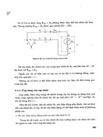
Figure 2: Accelerometer Position Relative to Gravity
Xout – This pin is the output of the x-axis acceleration
sensor. The user should ensure the load impedance is
sufficiently high as to not source/sink >250µA typical.
While the sensitivity of this axis has been programmed at
the factory to be the same as the sensitivity for the y-axis,
the accelerometer can be programmed for non-equal
sensitivities on the x- and y-axes. Contact the factory for
additional information.
X-Axis
Orientation
To Earth’s
Surface
(deg.)
Yout – This pin is the output of the y-axis acceleration
sensor. The user should ensure the load impedance is
sufficiently high as to not source/sink >250µA typical.
While the sensitivity of this axis has been programmed at
the factory to be the same as the sensitivity for the x-axis,
the accelerometer can be programmed for non-equal
sensitivities on the x- and y-axes. Contact the factory for
additional information.
DISCUSSION OF TILT APPLICATIONS AND
RESOLUTION
Tilt Applications: One of the most popular applications of
the MEMSIC accelerometer product line is in
tilt/inclination measurement. An accelerometer uses the
force of gravity as an input to determine the inclination
angle of an object.
A MEMSIC accelerometer is most sensitive to changes in
position, or tilt, when the accelerometer’s sensitive axis is
perpendicular to the force of gravity, or parallel to the
Earth’s surface. Similarly, when the accelerometer’s axis is
parallel to the force of gravity (perpendicular to the Earth’s
surface), it is least sensitive to changes in tilt.
X-Axis
90
85
80
70
60
45
30
20
10
5
0
X Output
(g)
Change
per deg.
of tilt
(mg)
Y-Axis
Y Output
(g)
-1.000
0.15
0.000
-0.996
1.37
0.087
-0.985
2.88
0.174
-0.940
5.86
0.342
-0.866
8.59
0.500
-0.707
12.23
0.707
-0.500
15.04
0.866
-0.342
16.35
0.940
-0.174
17.16
0.985
-0.087
17.37
0.996
0.000
17.45
1.000
Table 1: Changes in Tilt for X- and Y-Axes
Change
per deg.
of tilt
(mg)
17.45
17.37
17.16
16.35
15.04
12.23
8.59
5.86
2.88
1.37
0.15
Resolution: The accelerometer resolution is limited by
noise. The output noise will vary with the measurement
bandwidth. With the reduction of the bandwidth, by
applying an external low pass filter, the output noise drops.
Reduction of bandwidth will improve the signal to noise
ratio and the resolution. The output noise scales directly
with the square root of the measurement bandwidth. The
maximum amplitude of the noise, its peak- to- peak value,
approximately defines the worst case resolution of the
measurement. With a simple RC low pass filter, the rms
noise is calculated as follows:
Noise (mg rms) = Noise(mg/ Hz ) * ( Bandwidth( Hz) *1.6)
The peak-to-peak noise is approximately equal to 6.6 times
the rms value (for an average uncertainty of 0.1%).
Table 1 and Figure 2 help illustrate the output changes in
the X- and Y-axes as the unit is tilted from +90° to 0°.
Notice that when one axis has a small change in output per
degree of tilt (in mg), the second axis has a large change in
output per degree of tilt. The complementary nature of
these two signals permits low cost accurate tilt sensing to
be achieved with the MEMSIC device (reference
application note AN-00MX-007).
MEMSIC MXR7202GL/ML
Page 4 of 4
2004.03.15
USING THE MXR7202GL/ML WITH OPERATING
VOLTAGES OTHER THAN 5V
The MXR7202GL/ML is tested and specified at VDD=5V;
however, it can be powered with VDD as low as 2.7V or as
high as 5.25V. Some performance parameters will change
as the supply voltage is varied. The MXR7202GL/ML
output sensitivity will be linearly proportional to supply
voltage. At 3V the output sensitivity is 3.0/5.0* 312mV/g =
187.2 mV/g. The zero g bias output is also ratiometric, so
the zero g is normally equal to VDD/2 at all supply voltages.
EXTERNAL FILTERS
AC Coupling: For applications where only dynamic
accelerations (vibration) are to be measured, it is
recommended to ac couple the accelerometer output as
shown in Figure 3. The advantage of ac coupling is that
zero g offset variations from part to part and zero g offset
change over temperature can be eliminated. Figure 3 is a
HFP (high pass filter) with a –3dB breakpoint given by the
. In many applications it may be
equation: f = 1
2πRC
desirable to have the HFP –3dB point at a very low
frequency in order to detect very low frequency
accelerations. Sometimes the implementation of this HFP
may result in unreasonably large capacitors, and the
designer may turn to digital implementations of HFPs
where very low frequency –3dB breakpoints can be
achieved.
A OUTX
A OUTY
C
R
A O UTX
Filtered
Output
R
A O UTY
Filtered
Output
C
A O UTX
A O UTY
R
C
A OUTX
Filtered
Output
C
A OUTY
Filtered
Output
R
Figure 4: Low Pass Filter
POWER SUPPLY NOISE REJECTION
One capacitor is recommended for best rejection of power
supply noise (reference Figure 5 below). The capacitor
should be located as close as possible to the device supply
pin (VDD). The capacitor lead length should be as short as
possible, and surface mount capacitor is preferred. For
typical applications, the capacitor can be ceramic 0.1 µF.
Figure 5: Power Supply Noise Rejection
PCB LAYOUT AND FABRICATION SUGGESTIONS
1.
Figure 3: High Pass Filter
Low Pass Filter: An external low pass filter would be
useful in low frequency applications such as tilt or
inclination. The low pass filter limits the noise floor and
improves the resolution of the accelerometer. The low pass
filter shown in Figure 4 has a –3dB breakpoint given by the
. For the 200 Hz ratiometric output
equation: f = 1
2πRC
device filter, C=0.1µF and R=8kΩ, ±5%, 1/8W.
2.
3.
4.
5.
MEMSIC MXR7202GL/ML
Page 5 of 5
Liberal use of ceramic bypass capacitors is
recommended.
Robust low inductance ground wiring should be used.
Care should be taken to ensure there is “thermal
symmetry” on the PCB immediately surrounding the
MEMSIC device and that there is no significant heat
source nearby.
A metal ground plane should be added directly beneath
the MEMSIC device. The size of the plane should be
similar to the MEMSIC device’s footprint and be as
thick as possible.
Vias can be added symmetrically around the ground
plane. Vias increase thermal isolation of the device
from the rest of the PCB.
2004.03.15
MXR7202GL/ML TYPICAL PERFORMANCE CHARACTERISTICS (@ 25°C, unless otherwise specified)
VDD= 5V
40%
50%
35%
45%
PERCENT OF PARTS
PERCENT OF PARTS
VDD= 3V
30%
25%
20%
15%
10%
5%
40%
35%
30%
25%
20%
15%
10%
5%
0%
1.44
1.46
1.48
1.5
1.52
1.54
0%
2.42
1.56
45%
35%
40%
PERCENT OF PARTS
PERCENT OF PARTS
40%
30%
25%
20%
15%
10%
5%
1.46
1.48
1.5
1.52
1.54
2.47
2.50
2.53
2.55
2.58
Voltages
X-axis Zero g Bias Distribution at Xout, VDD=5V
Voltages
X-axis Zero g Bias Distribution at Xout, VDD=3V
0%
1.44
2.45
35%
30%
25%
20%
15%
10%
5%
0%
2.42
1.56
2.45
2.47
2.50
2.53
2.55
2.58
Voltages
Y-axis Zero g Bias Distribution at Yout, VDD=5V
Voltages
Y-axis Zero g Bias Distribution at Yout, VDD=3V
30%
18%
16%
25%
PERCENT OF PARTS
PERCENT OF PARTS
14%
12%
10%
8%
6%
4%
2%
0%
168
187
206
mV/g
X-axis Sensitivity Distribution at Xout, VDD=3V
MEMSIC MXR7202GL/ML
20%
15%
10%
5%
0%
287
311
335
mV/g
X-axis Sensitivity Distribution at Xout, VDD=5V
Page 6 of 6
2004.03.15
18%
35%
30%
14%
PERCENT OF PARTS
PERCENT OF PARTS
16%
12%
10%
8%
6%
4%
2%
0%
168
187
206
mV/g
Y-axis Sensitivity Distribution at Yout, VDD=3V
MEMSIC MXR7202GL/ML
25%
20%
15%
10%
5%
0%
287
311
335
mV/g
Y-axis Sensitivity Distribution at Yout, VDD=5V
Page 7 of 7
2004.03.15
LCC-8 PACKAGE DRAWING
Fig 6: Hermetically Sealed Package Outline
MEMSIC MXR7202GL/ML
Page 8 of 8
2004.03.15