- Trang chủ >>
- Khoa Học Tự Nhiên >>
- Vật lý
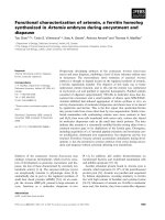
Characterization of tin catalyzed silicon nanowires synthesized by the hydrogen radical assisted deposition method
Bạn đang xem bản rút gọn của tài liệu. Xem và tải ngay bản đầy đủ của tài liệu tại đây (632.24 KB, 3 trang )
Characterization of Tin-catalyzed silicon nanowires synthesized by the hydrogen
radical-assisted deposition method
Minsung Jeon
⁎
, Hisashi Uchiyama, Koichi Kamisako
Department of Electronic and Information Engineering, Tokyo University of Agriculture and Technology, 2-24-16 Nakacho, Koganei, Tokyo 184-8588, Japan
abstractarticle info
Article history:
Received 11 September 2008
Accepted 2 October 2008
Available online 9 October 2008
Keywords:
Tin catalyst
Silicon nanowires
Hydrogen radicals
VLS mechanism
Phase diagram
Tin-catalyzed silicon nanowires (SiNWs) were synthesized at various hydrogen gas flow rates using the
hydrogen radical-assisted deposition method. Large quantities of SiNWs with various crystal phases were
synthesized and their characteristics were estimated. Tin-capped SiNWs were straightly grown and their
structures were changed with increasing hydrogen gas flow rates. Their diameters on the bottom side were
increased ranging from approximately 50 to 200 nm and their lengths extended up to ~2 µm with increasing
hydrogen gas flow rates.
© 2008 Elsevier B.V. All rights reserved.
1. Introduction
Since the synthesis of carbon nanotubes [1], much attempt has
been devoted to synthesizing one-dimensional nanostructure materi-
als, such as nanowires, nanorods, nanotubes and nanoribbons [2].
These nanomaterials provide a good system to research the depen-
dence of electrical, optical and magnetic properties [3–8]. They are
also expected to play an important role as both interconnections and
functional units in fabrication of e lectronic, optoelectronic and
electrochemical devices with low-dimensional structures. In recent
years, silicon nanowires (SiNWs) as one-dimensional structure have
attracted due to their unique mechanical and semiconducting
properties. SiNWs have been synthesized by using various methods,
such as chemical vapor deposition (CVD) [9], oxide-assisted [10],
template-assisted [11] and laser ablation method [12] via well-known
vapor–liquid–solid (VLS) mechanism [9,13]. Moreover, various metal
nanoparticles, such as Au, Al, Ga, Ti and Sn [9,14–17], have been
studied for synthesizing SiNWs. Among these, tin (Sn) appears to be
the favorable catalyst for low temperature synthesis from its phase
diagram, because the Sn–Si alloy has relatively low eutectic tempera-
ture as 232 °C [18]. The low melting point materials form eutectic with
silicon at low temperature and with extremely low content of the
elemental semiconductors. We have also reported a simple way to
synthesize SiNWs using the low-melting-point metal catalysts, such
as In and Ga, by the hydrogen radical-assisted deposition method
[19,20]. In particular, the synthesis of SiNWs with Sn catalyst, which
has relatively low eutectic temperature with Si, has been reported by a
few researchers [17,21]. Moreover, their properties are not well-
known yet. In this study, therefore, the SiNWs are synthesized using
Sn nanoparticles as catalyst at various growth conditions and their
characteristics are investigated.
2. Experimental
Tin (Sn) metal thin film as catalyst is evaporated on Corning #1737
glass substrates. Before metal film evaporation, the glass substrates are
cleaned in a bath containing acetone, ethanol and deionized water with
ultrasonic agitation for 5 min. The substrates are located in vacuum
chamber and Sn metal film approximately 100 nm is deposited. The Sn-
coated glass substrates are set and heated at 400 °C in the experimental
vacuum chamber with a pressure of 2×10
− 5
Torr. Hydrogen (H
2
) gas is
introduced into the 1/2-inch diameter trumpet-like quartz tube, which
is surrounded by microwave cavity. Then, the hydrogen radicals
generated by 2.45 GHz microwave are irradiated for 1 min onto the
samples to fabricate nanosize metal particles. To fabricate nanoparticles,
aH
2
gas flow, microwave power and working p ressure are selected to
100 sccm, 40 W and 0.5 Torr, respectively. For synthesizing silicon
nanowires (SiNWs), silane (SiH
4
) gas as Si source is introduced into the
experimental chamber from a ring-type copper tube that has many
orifices, and it is reacted with hydrogen radicals generated by
microwave in the quartz discharge tube. In order to investigate the
effect of synthesis conditions, SiNWs are synthesized using the
hydrogen radical-assisted deposition method [19] at various hydrogen
gas flow rates ranging from 130 to 180 sccm. Detailed other synthesis
conditions are summarized in Table 1 .
SiNWs are syn thesized for 1 0 min, and t heir characteristics a r e
estimated by Field Emission Scanning Electron Microscopy (FE-SEM) and
X -ra y diffractometer (XRD). For further investigation, the sy nthesized
Materials Letters 63 (2009) 246–248
⁎ Corresponding author. Tel./fax: +81 42 388 7446.
E-mail address: (M. Jeon).
0167-577X/$ – see front matter © 2008 Elsevier B.V. All rights reserved.
doi:10.1016/j.matlet.2008.10.005
Contents lists available at ScienceDirect
Materials Letters
journal homepage: www.elsevier.com/locate/matlet
SiNWs are remo ved onto a car bon copper grid. The detailed characteristics
of as-synthesized S iNWs are analyzed by a scanning transmission electron
microscopy (S- T EM) and an energy dispersive X -ray spectrometer (EDS) .
3. Results and discussion
Before synthesis of silicon nanowires (SiNWs ), hydrogen radical treatment is performed
on the Sn-coated substrate to fabricate Sn nanoparticles. The hydrogen radical tr eatment is
effective to o btain voluminous SiNWs. S ubseq uently, the SiNWs wer e s ynthesized a t various
hydrogen (H
2
)gasflow rates. In order t o investig ate the morphological property of as-
synthesized SiNWs at varied conditions, a FE-SEM observation was performed after
synthesis of SiNWs for 1 0 min at 400 °C.
Fig. 1 (a)–(c) shows the low-magnification FE-SEM images of the as-synthesized SiNWs
at va rious H
2
gas flow r a tes: (a ) 130 sccm, ( b) 150 sccm a nd (c ) 180 sccm. V o luminous S iNWs
were whisker-like ly synthesized at all growth conditions. Their structures were gradually
changed w ith i ncr easing H
2
gas flo w rate. When the SiNWs w ere synthesized at H
2
gas flow
of 13 0 s ccm, the SiNWs we re smoothly curved as shown in inset of Fig. 1 (a). On the other
hand, when the SiNWs w ere s ynthesized at above H
2
flow r ate of 1 30 sccm, the SiNWs were
straightly gr own a s shown in insets of Fig. 1 (b) a nd (c). How ever, their si zes became thicker
with increasing H
2
gas flo w. The diameters of SiNWs on the bottom side were gradually
increased ranging from approximat ely 50 t o 200 nm with increasing H
2
gas flow rates.
Moreover , their lengths extended up to ~2 µm. It indicates that the H
2
gas flow affect the
growth of SiNWs. Moreover, the high-magnification FE-SEM images explained that th e
SiNWs were tapered and that Sn catalysts r emained on the tip of Si NWs (see r ed c ircles i n
inset of Fig. 1 (a)). It means that the SiNWs a r e synthesized via vapor–liq uid–solid (VLS)
mechanism [9, 13]. The detailed explanation of the VLS mechanism will be followed later .
Above mentioned sampl es w ere also e xamined b y XRD measurement. Fig. 1 (d) s hows the
XRD p att erns of S iNWs synthesized a t varied H
2
gas flow r at es. The XRD patterns indicate that
the syn thesized SiNWs ar e highl y crystallized sil icon with di ffraction peaks of (111), (220)and
(3 11). Mor e over, the Snmetal peaks of (200) and (1 0 1) were also w eakly detected at 30.66 and
32.044 deg., r espectively (see black arrows in Fig. 1 ( d)). These peaks were reveal ed because
theSncatalystswerelocatedonthetopofSiNWsasshownininsetofFig. 1(a). Such SiNWs
grew randomly wi th different crystal orientations.
Fig. 2 shows a schematic of the Sn–Si alloy binary phase diagram [18]. SiNWs are
typically synthesized via the VLS growth mechanism at temperatures higher than the Sn–
Si eutectic temperature. This VLS mechanism has been introduced by Wagner et al. to
growth single crystalline silicon [9]. A typical VLS growth starts with the dissolution of
gaseous reactants into a nano-size metal liquid droplet, followed by nucleation and growth
Table 1
Synthesis conditions for silicon nanowires (SiNWs)
H
2
flow [sccm] SiH
4
flow [sccm] M.W.P [W] Press. [Torr] Temp. [°C] Time [min]
130–180 12 40 0.5 400 10
Fig. 1. FE-SEM images of the as-synthesized SiNWs at hydrogen gas flow of (a) 130 sccm, (b) 150 sccm and (c) 180 sccm. All the scale bars represent 2.5 µm. (d) XRD patterns of the as-
synthesized SiNWs at various hydrogen gas flow rates.
Fig. 2. Schematic of the Sn–Si alloy binary phase diagram.
247M. Jeon et al. / Materials Letters 63 (2009) 246–248
of crystalline wires. Here, the Sn nanoparticles and decomposed SiH
4
are typical metal
catalyst and silicon source used to synthesize SiNWs. The fabricated Snnanoparticles after
hydrogen radical treatment provide energetically favored Sn–Si sites for the adsorption of
incoming vapor silicon sources. The adsorbed Si atoms diffused into the liquid Sn
nanoparticles, which results in the formation of a Sn–Si alloy. The continued adsorption of
the Si sources into the Sn–Si alloy liquid droplets leads to the supersaturation of the Sn–Si
eutectic in a broad region above 230 °C, which results in the growth of a solid Si nucleus.
TheSnnanoparticlesarepushedawayfromthesubstratebycontinuousSisourcefeeding
in the liquid–solid interface and it is lifted upward by the growing SiNWs. As a result, large
quantities of SiNWs are synthesized.
The detailed compositions of as-synthesized SiNWs via VLS mechanism were
examined by S-TEM and EDS measurement. Fig. 3(a)–(c) shows a high-magnification
SEM image of as-synthesized Si nanowire and corresponding EDS analysis. The S-TEM
micrograph in inset of Fig. 3(a) represents the Si nanowire capped by a catalyst
nanoparticle. The EDS measurement was operated during the S-TEM observation. The
EDS analysis carried out on the nanowire stem and metal nanoparticle. As can be seen in
Fig. 3(b), the Si nanowire comprises only Si element. The other peaks, such as C and Cu,
were also detected. It is attributed to the effect of the TEM grid. Fig. 3(c) shows the EDS
spectra taken for the nanoparticle shown in inset of Fig. 3(a). It indicates that the
nanoparticle comprises Sn and Si elements. The Sn nanoparticle located on the top of Si
nanowire implies that a Sn catalyst assisted VLS mechanism is typically related in the
growth of SiNWs. These results denote that the as-synthesized SiNWs by ourexperimental
method are pure crystalline silicon without oxygen and other impurities.
4. Conclusion
Tin-catalyzed silicon nanowires (SiNWs) were synthesized atvarious
hydrogen gas flow rates using the hydrogen radical-assisted deposition
method. Voluminous SiNWs, which have various crystal phases, were
whisker-likely synthesized at all growth condition. Their structures
were gradually changed with increasing hydrogen gas flow rate. The
diameters of SiNWs on the bottom side were increased ranging from
approximately 50 to 200 nm and their lengths extended up to ~2 µm. It
indicates that the SiNWs can be controlled by the introduced hydrogen
gas flow rates.
References
[1] Iijima S. Nature 1991;354:56.
[2] Wang ZL. Nanowires and Nanobelts: Materials, Properties and Devices. Kluwer
Academic Publishers; 2003.
[3] Westwater J, Gosain DP, Usui S. Jpn J Appl Phys 1997;36:6204.
[4] Alivisatos AP. Science 1996;271:933.
[5] Kang SH, Kim JY, Kim HS, Sung YE. J Ind Eng Chem 2008;14:52.
[6] Cui Y, Lieber CM. Science 2001;291:851.
[7] Chung SW, Yu JY, Heath JR. Appl Phys Lett 2000;76:2068.
[8] Duan X, Niu C, Sahi V, Chen J, Parce JW, Empedocles S, et al. Nature 2003;425:274.
[9] Wagner RS, Ellis WC. Appl Phys Lett 1964;4:89.
[10] Wang N, Tang YH, Zhang YH, Lee CS, Bello I, Lee ST. Chem Phys Lett 1999;299:237.
[11] Zhang XY, Zhang L, Meng GW, Li GH, Phillipp NY, Phillipp F. Adv Mater 2001;13:1238.
[12] Morals AM, Lieber CM. Science 1998;279:208.
[13] Givargizov EI. J Cryst Growth 1975;31:20.
[14] Wang Y, Schmidt V, Senz S, Gosele U. Nat Nanotechnol 2006;1:186.
[15] Sunkara MK, Sharma S, Miranda R, Lian G, Dickey EC. Appl Phys Lett 2001;79:1546.
[16] Kamins TI, Williams RS, Chen Y, Chang YL, Chang YA. Appl Phys Lett 2000;76:562.
[17] Chen ZH, Jie JS, Luo LB, Wang H, Lee CS, Lee ST. Nanotechnology 2007;18:345502.
[18] Olesinski RW, Abbaschian GJ. Bull Alloy Phase Diagr 1984;5:273.
[19] Jeon MS, Kamisako K. Mater Lett 2008;62:3903.
[20] Jeon MS,Tomitsuka Y,Kamisako K. J Ind Eng Chem 2008. doi:10.1016/j.jiec.2008.06.004.
[21] Shao M, Hui H, Li M, Ban H, Wang M, Jiang J. Chem Commun 2007;8:793.
Fig. 3. (a) S-TEM micrograph of the silicon nanowire capped by a Sn catalyst
nanoparticle. (b) and (c) represent the corresponding EDS spectra taken from the
nanowire stem and the catalyst nanoparticle, respectively.
248 M. Jeon et al. / Materials Letters 63 (2009) 246–248