- Trang chủ >>
- Khoa Học Tự Nhiên >>
- Vật lý
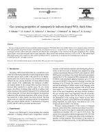
gas sensor response of pure and activated wo3 nanoparticle
Bạn đang xem bản rút gọn của tài liệu. Xem và tải ngay bản đầy đủ của tài liệu tại đây (431.72 KB, 7 trang )
Sensors and Actuators B 117 (2006) 128–134
Gas sensor response of pure and activated WO
3
nanoparticle
films made by advanced reactive gas deposition
L.F. Reyes
a,∗,1
, A. Hoel
a
, S. Saukko
b
, P. Heszler
a,2
, V. Lantto
b
, C.G. Granqvist
a
a
Department of Engineering Sciences, The
˚
Angstr¨om Laboratory, Uppsala University, P.O. Box 534, SE-75121 Uppsala, Sweden
b
Microelectronics and Materials Physics Laboratories, University of Oulu, Linnanmaa, FIN-90570 Oulu, Finland
Received 6 July 2005; received in revised form 2 November 2005; accepted 7 November 2005
Available online 7 December 2005
Abstract
Pure and activated (doped) nanocrystalline WO
3
films, produced by advanced reactive gas deposition, were investigated for gas sensing appli-
cations. Activation took place by co-evaporation of Al or Au with tungsten oxide as the particles were produced. Structural characterization of
the films was performed by electron microscopy and X-ray diffractometry. Sensitivity, response time, and recovery time of the sensors were
systematically investigated as a function of annealing and operating temperature, using H
2
S, CO, and NO
2
as test gases. The sensitivity was found
to lie below and around the ppm level for H
2
S and NO
2
, respectively.
© 2005 Elsevier B.V. All rights reserved.
Keywords: Microstructure; Electrical properties; WO
3
; Au; Sensor
1. Introduction
Nanocrystalline materials are in the focus of contemporary
materials research as a consequence of the superior properties
that are achievable when materials are built up from structural
units with sizes on the nanometer scale [1]. Materials of this
type can be produced by a variety of techniques including gas
deposition [2], sputtering [3], sol–gel technology [4], microbi-
ological preparation [5], etc. Gas-phase synthesis stands out as
being of particular interest [6].
Materials consisting of crystalline nanoparticles with a
porous structure can have extremely large surface areas and be
well suited for applications in semiconductor-based gas sensors.
For example, it has been recently shown that nanocrystalline
WO
3
films exhibit very interesting sensor properties and are
candidates for detecting toxic gases such as H
2
S [7],NO
2
[8],
and ozone [9]. The sensor properties can be boosted by activa-
tion with metals such as Au, Pd, and Pt [10]. The purpose of
∗
Corresponding author. Tel.: +51 1 2922528.
E-mail address: (L.F. Reyes).
1
Permanent address: Facultad de Ciencias, Universidad Nacional de Inge-
nier
´
ıa, Av. T
´
upac Amaro 210, CP 31-139 Lima, Peru.
2
Also at Research Group on Laser Physics of Hungarian Academy of Sci-
ences, P.O. Box 406, H-6701 Szeged, Hungary.
activation is to improve the sensitivity as well as the selectiv-
ity of the sensor films for the gas to be detected. We note that
nanocrystalline WO
3
is well known also as an electrochromic
material capable of sustaining reversible and persistent changes
of its optical properties [11,12]. Analogously with the case for
sensors, the electrochromic properties can be radically changed
by inclusion of Au nanoparticles [13].
Below we present results from a study on gas sensing using
nanocrystalline films of WO
3
in pure (intrinsic) form and after
activation with Au or Al. The films were prepared by reactive gas
deposition. Materials characterization was accomplished by X-
ray diffraction (XRD) and scanning electron microscopy (SEM).
The performance of sensor devices, based on the WO
3
films, was
investigated by a two-point measuring system capable of in situ
conductivity determinations as a function of sensor temperature
and gas concentration. Test gases of H
2
S, NO
2
, and CO were
used at different concentrations on the ppm level.
2. Experimental details
A reactive gas deposition unit (Ultra Fine Particle equip-
ment, ULVAC Ltd., Japan) was used for producing nanocrys-
talline WO
3
-based films. A detailed description of this unit was
given elsewhere [14]. Briefly, the system consists of an evap-
oration chamber, a deposition chamber, a transfer pipe, and an
0925-4005/$ – see front matter © 2005 Elsevier B.V. All rights reserved.
doi:10.1016/j.snb.2005.11.008
L.F. Reyes et al. / Sensors and Actuators B 117 (2006) 128–134 129
evacuation pipe. The chambers were evacuated to a base pressure
of ∼3 × 10
−2
mbar prior to the experiments. For producing WO
3
nanoparticles, a tungsten pellet was placed inside an induction
coil in the evaporation chamber and was heated up to ∼1200
◦
C.
Reactive evaporation was performed using synthetic air (80% N
2
and 20% O
2
) introduced with a flow of 10 l/min at the bottom
of the induction coil so that an operating pressure of ∼20 mbar
was maintained. The surface of the tungsten pellet was oxidized,
and the chosen temperature allowed vaporization of the tung-
sten oxide layer. The gas flow moved the tungsten oxide vapor
upward, leading to a cooling of the vapor as it was removed
from the heating zone and thereby yielding first molecular oxide
clusters and then WO
3
nanoparticles. One part of the gas flow
in the nanoparticle formation zone was diverted by the transfer
pipe to the deposition chamber. This selection, and the fact that
the gas flow is highly laminar, results in a narrow size distribu-
tion of the particles [15,16]. For producing the activated WO
3
nanoparticle films, additional Au or Al pellets were placed in the
heating zone, thus resulting in co-evaporation or sublimation of
the metallic dopant. Doping was manifest as a color induced in
the film, which made the visual impression different from that of
the unactivated WO
3
nanoparticle films. Both unactivated and
activated WO
3
films were deposited on alumina substrates with
previously prepared gold electrodes, separated by 0.3 mm, on
the front side and a platinum wire heater on the back side. Sam-
ples were heat treated at temperatures between 100 and 600
◦
C
for 1 h to examine the annealing effect on the sensitivity of the
WO
3
nanoparticle films.
Thickness measurements were made by a Tencor Alpha-Step
200 mechanical stylus instrument with a maximal resolution of
0.5 nm. An average thickness of 11 m was found for the as-
prepared films. The crystal structure of the deposited materials
was examined by X-ray diffraction, using a Siemens D5000
diffractrometer (40 kV, 40 mA) with monochromatized Cu K␣
radiation having a wavelength of 1.5406
˚
A. The mean grain size
was determined using Scherrer’s equation [17]. Microstructures
of the nanocrystalline WO
3
films were investigated by scanning
electron microscopy using a LEO 1550 Gemini instrument with
an in-lens detector.
The conductance of the samples was measured by a two-
point set-up in an evacuated system comprising a gas source, a
gas blender (Signal series 850), and a test chamber. Synthetic
air was used as a carrier gas at a constant flow rate 1 l/min.
Diverse parameters – such as sensor temperature, gas concen-
tration, exposition time to different gases, etc. – were computer
controlled and monitored in real time.
3. Results and discussion
3.1. XRD analysis
Fig. 1 shows X-ray diffraction patterns of as-deposited and
annealed (sintered) nanocrystalline WO
3
films. Reflection peaks
due to tetragonal (t) and monoclinic (m) phases of WO
3
and of
the substrate (Al
2
O
3
) can be seen. Clearly the WO
3
films con-
sist of a mixture of tetragonal and monoclinic phases. It should
be noted, though, that films produced at low heating powers
Fig. 1. X-ray diffractograms of nanocrystalline WO
3
films on alumina sub-
strates in as-deposited state and after sintering at a temperature T between 100
and 600
◦
C. Peaks denoted by m, t, and (*)Al
2
O
3
are characteristic for the mon-
oclinic and tetragonal phases of WO
3
and for the alumina substrate, respectively.
only gave evidence for the tetragonal phase [7,18]. The tetrag-
onal structure corresponds to a high-temperature phase of WO
3
that is stable above 740
◦
C, while a monoclinic phase is stable
at lower temperatures. It is evident that the high temperature
associated with the W oxide evaporation – being ∼1200
◦
C
during film fabrication – can lead to a tetragonal phase which
remains metastable during cooling in the gas stream. No sig-
nificant changes in the diffractograms could be observed for
sintering temperatures up to 300
◦
C. However, the tetragonal
phase started to transform to monoclinic above 300
◦
C, and only
the monoclinic phase appeared to be present at a sintering tem-
perature of 600
◦
C. The crystallite grain size was ∼10 nm for
the as-deposited films, and no grain growth could be seen up
to 300
◦
C. However, grain growth could be observed above this
temperature, and the crystallite size was ∼40 nm at 600
◦
C.
3.2. SEM analysis
Scanning electron microscopy data on as-deposited
nanocrystalline WO
3
films are shown in Fig. 2. A minimum
feature size of ∼12 nm can be seen, which is in agreement
with XRD measurements analyzed by using Scherrer’s equa-
tion. Aggregates in a porous network-like structure could be
observed; this is an important characteristic for gas sensors [19].
Fig. 2. Scanning electron micrograph (inset with higher magnification) of an
as-deposited nanocrystalline WO
3
film.
130 L.F. Reyes et al. / Sensors and Actuators B 117 (2006) 128–134
Transmission electron microscopy data on samples produced at
slightly lower temperatures were reported elsewhere [18].
4. Sensitivity measurements
The sensitivity of the active layer upon gas exposure was
defined as the ratio G
gas
/G
air
, where G
gas
and G
air
denote the
conductance of the sensor exposed to a test gas (H
2
S, NO
2
,
or CO) and in pure synthetic air, respectively. First the pure
nanocrystalline WO
3
films, sintered at temperatures between
100 and 600
◦
C, were tested upon exposure to 10 ppm of H
2
S
at room temperature. Fig. 3 shows that the sample annealed at
300
◦
C displayed the highest sensitivity.
Fig. 4(a) depicts room-temperature sensitivity upon 10 min
exposures to several concentrations of H
2
S gas of a sample sin-
tered at 300
◦
C. This exposure produced a drastic increase of
the sensitivity; specifically an increment by more than three
orders of magnitude can be observed at 35 ppm of H
2
S. One can
also note that the increase in sensitivity does not reach satura-
tion for the applied concentration range, between 5 and 35 ppm,
but the sensitivity increases linearly with the H
2
S concentration
as apparent from Fig. 4b. The slope of the sensitivity curve is
somewhat below 100 per ppm, indicating sensitivity below the
ppm level for H
2
S at room temperature. However, the change
of the sensitivity as a function of time was very slow at room
temperature; the response time was several minutes, and the
recovery time amounted to some hours after evacuation of the
gas. However, high-temperature operation at 600 K significantly
improved the response and recovery times of the sensors (see
Fig. 5a), but there is a concomitant decrease of the sensitivity
by more than two orders of magnitude compared to the case of
room-temperature operation (see Fig. 5b). The sensitivity always
reached its initial value after the H
2
S gas had been evacuated,
which shows that the adsorption and desorption processes were
reversible under cycles of gas exposure and ensuing evacuation.
A slightly non-linear behavior of the sensitivity versus H
2
S con-
centration was apparent at 600 K (see Fig. 5b).
Fig. 3. Sensitivity as a function of annealing temperature for a pure nanocrys-
talline WO
3
sensor exposed to 10 ppm of H
2
S at room-temperature operation.
The line is a guide for the eye.
Fig. 4. (a) Sensitivity as a function of time for a pure nanocrystalline WO
3
sensor (sintered at 300
◦
C) exposed to several H
2
S concentrations at room-
temperature operation. H
2
S injection and evacuation took place after 5 and
15 min, respectively. (b) Sensitivity S (maximum values) as a function of H
2
S
concentration C for the experiment described in (a). The line corresponds to the
stated equation.
A comparison of the room-temperature sensitivity for as-
deposited unactivated and activated films is presented in Fig. 6.
Clearly the WO
3
nanoparticle film activated by Al exhibited
a sensitivity increase by more than one order of magnitude,
while activation with Au increased the sensitivity approximately
by a factor of two. Neither the concentration nor phase of the
dopant was investigated in this study, but it is likely that the
Al co-evaporation resulted in an inclusion of aluminum oxide.
Sensitivity measurements are in progress to determine optimal
concentrations of the activation material.
Slow response and long recovery time prevailed for room-
temperature operation of activated films (see Fig. 6), just as for
unactivated films (see Fig. 4a). However, these characteristics
could be significantly improved by having the sensor oper-
ate at higher temperature (see Fig. 7a and b). Fig. 7a shows
that the processes of adsorption and desorption were reversible
for several concentrations of H
2
S gas at 600 K. We note that
these processes were irreversible for continued H
2
S exposures in
10 min-intervals for the 300–450 K temperature range. It is also
observed that Au is a better dopant for high-temperature oper-
ation than Al, contrary to the situation for room-temperature
sensing (see Fig. 6). A slight non-linearity can be seen in the
sensitivity versus concentration curves (see Fig. 7b).
L.F. Reyes et al. / Sensors and Actuators B 117 (2006) 128–134 131
Fig. 5. (a) Sensitivity as a function of time for a pure nanocrystalline WO
3
film
(sintered at 300
◦
C) exposed to several H
2
S concentrations at 600 K operation
temperature. The solid lines represent the H
2
S concentration (right-hand scale),
while the dotted curves denote measured data (left-hand scale). (b) Sensitivity
S as a function of H
2
S concentration C for the experiment described in part (a).
The curve corresponds to the stated equation.
Fig. 8 depicts the conductance response of an Au-activated
sensor film under exposure to CO and NO
2
gases at an
operating temperature of 700 K. For a reducing gas such
as CO, the conductance was increased, while a conductance
Fig. 6. Sensitivity as a function of time for pure and activated as-deposited
nanocrystalline WO
3
sensors upon exposure to 10 ppm H
2
S at room-temperature
operation. H
2
S injection and evacuation took place after 5 and 15 min, respec-
tively.
Fig. 7. (a) Sensitivity as a function of time for pure and activated as-deposited
nanocrystalline WO
3
sensors exposed to several H
2
S concentrations at 600 K
operation temperature. Solid bars represent H
2
S concentrations (right-hand
scale), while curves represent measured data (left-hand scale). (b) Sensitivity
as a function of H
2
S concentration for the experiments described in (a).
decrease could be observed for an oxidizing gas such as
NO
2
.
In order to determine the optimal operating temperature, the
sensitivity of an Al-activated sensor film was tested at different
operation temperatures in H
2
S, CO, and NO
2
. Results are shown
in Fig. 9 for gas concentrations being 10 ppm H
2
S, 100 ppm
CO, and 5 ppm NO
2
. The sensor exhibited different optimum
operating temperatures, specifically being 400, 525, and 700 K
for H
2
S, NO
2
, and CO, respectively. Importantly, the sensor did
Fig. 8. Conductance response of an as-deposited Au-activated WO
3
sensor upon
CO (50 and 100 ppm) and NO
2
(5 and 10 ppm) exposures at 700 K operating
temperature.
132 L.F. Reyes et al. / Sensors and Actuators B 117 (2006) 128–134
Fig. 9. Sensitivity as a function of operating temperature for as-deposited Al-
activated WO
3
films exposed to 10 ppm H
2
S (right-hand scale), 5 ppm NO
2
(left-hand scale), and 100 ppm CO (left-hand scale). The lines are guide for the
eye.
not show any overlap in its maximum gas-specific sensitivities,
which implies that chemical selectivity can be obtained when the
sensor is operated at 400, 525, and 700 K. At optimal operating
temperatures, the sensor is ∼20 and ∼2000 times more sensitive
to H
2
S than to NO
2
and CO, respectively, normalized to the
concentration.
5. Discussion
Semiconductor gas sensors are mostly used at in air at atmo-
spheric pressure, so that the surface of the sensor is continuously
exposed to oxygen with a partial pressure of ∼0.2 atm. Stud-
ies on the operating mechanism of semiconductor gas sensors
indicated that most target gases are detected via the influence
they exert on the adsorbed oxygen [20]. In particular, several
investigations showed that the key reaction for detecting reduc-
ing gases involves oxygen ions on the surface of the sensor
[19].
We first consider processes that are – or at least may be –
responsible for conductivity changes in sensor films. At low
temperatures, it has been suggested [20] that resistance changes
due to H
2
S adsorption occur as a consequence of the reactions
O
2
(g) + e
−
↔ O
2
−
(ads) (1)
2H
2
S(g) + 3O
2
−
(ads) ↔ 2H
2
O + 2SO
2
+ 3e
−
(2)
where (g) and (ads) denote gas phase and adsorbed species,
respectively. Reaction (1) takes place prior to sensing and creates
a thin electron-depleted layer at the surfaces of the WO
3
grains.
As H
2
S is adsorbed, electrons are released into the conduction
band according to reaction (2), resulting in conductivity and
thus sensitivity increase. For high-temperature operation, the
reactions
O
2
−
(ads) + e
−
↔ 2O
−
(ads) (3)
H
2
S(ads) + O
−
(ads) ↔ H
2
O + S + e
−
(4)
are relevant [20]. Reaction (3) assumes that O
2
−
has already
been formed on the surface by reaction (1).
Another mechanism, that can play a role in the gas sensing,
is the formation of additional surface oxygen vacancies, created
by the interaction of H
2
S with lattice oxygen according to [21]
3WO
3
+ 7H
2
S → 3WS
2
+ SO
2
+ 7H
2
O (5)
This reaction takes place on the surface and involves a reduction
of W
6+
to W
4+
. Oxygen leaves the surface thereby releasing
electrons into the grains so that the conductivity of the film is
increased. However, re-oxidation of the vacancies by O
2
results
in a competition with the formation of the oxygen vacancies by
H
2
S.
Samples sintered at 300
◦
C exhibited the largest sensitivity.
This may be associated with structural modifications, shown by
the XRD analysis which indicated that a transformation from
a tetragonal to a monoclinic phase commenced at ∼300
◦
C. It
therefore appears that a certain ratio of tetragonal to monoclinic
phase is required for optimal sensitivity.
The high sensitivity at room temperature is remarkable and in
accordance with earlier results of ours [22]. It may be explained
as a consequence of several different effects such as (i) the occur-
rence of a tetragonal phase of WO
3
in the film [22]; (ii) a high
surface area of the nanocrystalline films; and (iii) a porous struc-
ture with percolating networks that can be extremely sensitive
to minor changes in the conductivity of the individual nanopar-
ticles ensuing from H
2
S adsorption.
The room-temperature sensitivity could be increased by
active materials, especially by Al as found from Fig. 6. Although
we could not identify the pertinent phase of Al, it is very likely
that it was in oxide form in the films since the Al evaporation took
place in synthetic air. It is known that Al
2
O
3
can be active for
oxygen adsorption in an air ambient [23], and it follows that it can
exert a catalytic role for reaction (1) in the WO
3
layers. Thisleads
to a lower intrinsic conductivity for the Al-doped films than for
the non-activated ones. According to reaction (2),H
2
S exposure
increases the conductivity of the sensor. In addition, active Al-
oxide centers can be neutralized by water produced by reaction
(2), thus resulting in further conductivity increase. Considera-
tions ofthis kind may explain theenhanced sensing capability for
the Al-doped films at room temperature. For high-temperature
sensing, the significant water desorption makes the neutraliza-
tion of the active Al oxide centers less effective, thereby yielding
less sensitivity than at low-temperature operation.
For room-temperature sensing, the long response times can
be explained by the slow reaction rate of H
2
S with adsorbed
oxygen ions (reaction (2)), and the long recovery time is due
to incomplete desorption of the adsorbed reaction products and
H
2
S after finishing the H
2
S exposure. By increasing the temper-
ature, the reactions described by (1) and (2) as well as desorption
of the products are faster, according to an Arrhenius-type behav-
ior, which explains the decrease of the response time as well
as the recovery time (see Fig. 7a). However, both pure and
activated WO
3
nanoparticle films exhibit low sensitivity for
high-temperature operation, as found from Fig. 7b. In addition,
Au-activated films were more sensitive than Al-activated ones
– in contrast to the behavior at room temperature (see Fig. 6)–
indicating that the catalytic effects are temperature sensitive.
L.F. Reyes et al. / Sensors and Actuators B 117 (2006) 128–134 133
Several reasons can be given for the sensitivity loss at high
temperatures. The rates of the reactions (3) and (4) become sig-
nificant at high temperatures and as a consequence – although
the net result of these reactions is neutral in terms of the number
of electrons – the involved electrons tend to block reaction (2) so
that fewer electrons are injected into the conduction band, thus
leading to a loss of sensitivity. Formation of hydrogen tungsten
bronze upon exposure to H
2
S may also contribute to the sensitiv-
ity loss at high temperatures. Similar effects have been reported
in electrochromic tungsten oxide [11,12]. It is also worth noting
that transformation to WS
2
occur for WO
3
powder reacting with
H
2
S at atmospheric pressure and elevated temperature according
to reaction (5) [24]. This implies that the amount of surface-
adsorbed oxygen available for reaction’s (2) and (4) decreases,
i.e., a thin layer containing W
S bonds works as an inhibitor,
which would result in lesssensitivity. The decrease of the amount
of the tetragonal phase as the operating temperature was elevated
may also contribute to the sensitivity loss [22]. Furthermore, the
desorption rate for adsorbed O
2
−
ions is accelerated at high tem-
peratures, thus leading to less sensitivity toward H
2
S according
to reaction (2).
The WO
3
nanoparticle sensor films are also sensitive to
CO and NO
2
at 700 K, as seen from Fig. 9. The conductivity
increased for CO exposure while it decreased for NO
2
expo-
sure. Reactions similar to those described by (1)–(4) above can
be used to account for the conductivity increase due to CO. As
the molecule is adsorbed, it is oxidized to CO
2
by the help of
an adsorbed
1
2
O
2
−
, thereby leaving one electron to the conduc-
tion band. Adsorption of NO
2
on WO
3
nanoparticles results in
a decrease of the conductivity, which may be explained by the
reactions [25]
NO
2
(g) + e
−
↔ NO
2
−
(ads) (6)
NO
2
(g) + e
−
↔ NO(g) + O
−
(ads) (7)
Both of these reactions require electrons from the conduction
band of WO
3
, which then leads to a decrease of the conductivity.
It is very likely that the reactions indicated for the various test
gases have different rates depending on the operating tempera-
ture. This may lead to different optimal operating temperatures
and, indeed, these temperatures were found to be 400 K for H
2
S,
525 K for NO
2
, and700 K for CO, as seen from Fig. 9. It is impor-
tant to observe that this effect, with no noticeable cross-over, can
be exploited for chemical selectivity.
6. Conclusions
Pure and activated nanocrystalline WO
3
films were pro-
duced by advanced reactive gas deposition on alumina substrates
prepared for gas sensor application. Activation took place by
co-evaporation of Al and Au with the tungsten source. As-
deposited films exhibited ∼10 nm average crystal size, high
electrical resistivity, and tetragonal structure. Agglomerates of
WO
3
nanoparticles with a porous structure – hence being suit-
able for gas sensing – could be observed by electron microscopy.
The tetragonal phase changed gradually to a monoclinic phase
as the sintering temperature was elevated from 100 to 600
◦
C.
Importantly, the WO
3
-nanoparticle-based sensors were sensitive
to H
2
S even at room temperature. However, room-temperature
operation resulted in a slow response (some minutes) and a long
recovery time (several hours). Both of these times could be sig-
nificantly decreased by operating at elevated temperature.
Activation by Al or Au increased the sensitivity of the WO
3
nanoparticle-based devices by about an order of magnitude. It
was also found that the activity of the dopants is temperature
dependent. Al is more effective at room temperature, while Au
is preferable at high-temperature operation. The sensitivity of
the sensors was measured for different test gases and at various
temperatures. The optimum sensing temperatures for H
2
S, NO
2
,
and CO were 400, 525, and 700 K, respectively. There is no
significant cross-over in the sensitivity curves for the three test
gases, thus pointing at chemical selectivity. The sensitivity of
the sensors is below and around the ppm level for H
2
S and NO
2
,
respectively.
Acknowledgement
One of us (L.F.R.) thanks the International Science Pro-
gramme of Uppsala University for a scholarship which made
it possible to carry out Ph.D. work at Uppsala University and at
the University of Oulu.
References
[1] H. Gleiter, Nanostructured materials: state of the art and perspectives,
Nanostruct. Mater. 6 (1995) 3.
[2] R. Uyeda, Studies of ultrafine particles in Japan: crystallography meth-
ods of preparation and technological applications, Prog. Mater. Sci. 35
(1991) 1.
[3] J. Rodr
´
ıguez, M. G
´
omez, J. Lu, E. Olsson, C.G. Granqvist, Reac-
tively sputter-deposited titanium oxide coatings with parallel penniform
microstructure, Adv. Mater. 12 (2000) 341.
[4] L.C. Klein (Ed.), Sol–Gel Optics: Processing and Applications, Kluwer,
Dordrecht, The Netherlands, 1994.
[5] R. Joerger, T. Klaus, C.G. Granqvist, Biologically produced
silver–carbon composite materials for optically functional thin-film coat-
ings, Adv. Mater. 12 (2000) 407.
[6] C.G. Granqvist, L.B. Kish, W.H. Marlow (Eds.), Gas Phase Nanoparticle
Synthesis, Kluwer, Dordrecht, The Netherlands, 2004.
[7] J.L. Solis, A. Hoel, V. Lantto, C.G. Granqvist, Infrared spectroscopy
study of electrochromic nanocrystalline tungsten oxide films made by
reactive advanced gas deposition, J. Appl. Phys. 89 (2001) 2727.
[8] D S. Lee, S D. Han, J S. Huh, D D. Lee, Nitrogen oxides-sensing
characteristics of WO
3
-based nanocrystalline thick film gas sensor, Sens.
Actuators B 60 (1999) 57.
[9] K. Aguir, C. Lemire, D.B.B. Lollman, Electrical properties of reactively
sputtered WO
3
thin films as ozone gas sensor, Sens. Actuators B 84
(2002) 1.
[10] M. Penza, C. Martucci, G. Cassano, NO
x
gas sensing characteristics of
WO
3
thin films activated by noble metals (Pd, Pt, Au) layers, Sens.
Actuators B 50 (1998) 52.
[11] C.G. Granqvist, Handbook of Inorganic Electrochromic Materials, Else-
vier, Amsterdam, The Netherlands, 1995.
[12] C.G. Granqvist, Electrochromic tungsten oxide films: review of progress
1993–1998, Sol. Energ. Mater. Sol. C 60 (2000) 201.
[13] T. He, Y. Ma, Y. Cao, W. Yang, J. Yao, Enhanced electrochromism of
WO
3
thin film by gold nanoparticles, J. Electroanal. Chem. 514 (2001)
129.
[14] L.F. Reyes, S. Saukko, A. Hoel, V. Lantto, C.G. Granqvist, Struc-
ture engineering of WO
3
nanoparticles for porous film applications
134 L.F. Reyes et al. / Sensors and Actuators B 117 (2006) 128–134
by advanced reactive gas deposition, J. Eur. Ceram. Soc. 24 (2004)
1415.
[15] J. S
¨
oderlund, L.B. Kiss, G.A. Niklasson, C.G. Granqvist, Lognormal size
distributions in particle growth processes without cuagulation, Phys. Rev.
Lett. 80 (1998) 2386.
[16] A. Hoel, J. Ederth, J. Kopniczky, P. Heszler, L.B. Kish, E. Olsson, C.G.
Granqvist, Conduction invasion noise in nanoparticle WO
3
/Au thin-film
devices for gas sensing application, Smart Mater. Struct. 11 (2002) 640.
[17] B.D. Cullity, Elements of X-ray Diffraction, Addison-Wesley, Reading,
MA, USA, 1956.
[18] A. Hoel, L.F. Reyes, S. Saukko, P. Heszler, V. Lantto, C.G. Granqvist,
Gas sensing with films of nanocrystalline WO
3
and Pd made by
advanced reactive gas deposition, Sens. Actuators 105 (2005) 283.
[19] S.R. Morrison, The Chemical Physics of Surfaces, Plenum, New York,
USA, 1978.
[20] P.T. Moseley, J.O.W. Norris, D.E. Williams, Technique and Mechanism
in Gas Sensing, Adam Hilger, Bristol, UK, 1991.
[21] A. Katrib, F. Hemming, P. Wehrer, L. Hilaire, G. Maire, The multi-
surface structure and catalytic properties of partially reduced WO
3
,WO
2
and WC + O
2
orW+O
2
as characterized by XPS, J. Electron Spectrosc.
76 (1995) 195.
[22] J.L. Solis, S. Saukko, L.B. Kish, C.G. Granqvist, V. Lantto, Nanocrys-
talline tungsten oxide thick-films with high sensitivity to H
2
S at room
temperature, Sens. Actuators B. 77 (2001) 316.
[23] L. Salvati, L.E. Makovsky, J.M. Stencel, F.R. Brown, D.M. Hercules,
Surface spectroscopic study of tungsten-alumina catalysts using X-ray
photoelectron, ion scattering, and Raman spectroscopies, J. Phys. Chem.
85 (1981) 3700.
[24] B. Ampe, J.M. Lovey, D. Thomas, G. Tridot, Contribution
`
al’
´
etude
des syst
`
emes: tungst
`
ene-oxyg
`
ene et tungst
`
ene-vanadium-oxyg
`
ene, Rev.
Chim. Min. 5 (1968) 801.
[25] O.V. Safonova, G. Delabouglise, B. Chenevier, A.M. Gaskov, M. Labeau,
CO and NO
2
gas sensitivity of nanocrystalline tin dioxide thin films
doped with Pd, Ru and Rh, Mater. Sci. Eng. C 21 (2002) 105.