Báo cáo " Implementation of the digital phase-sensitive system for low signal measurement " docx
Bạn đang xem bản rút gọn của tài liệu. Xem và tải ngay bản đầy đủ của tài liệu tại đây (926.39 KB, 6 trang )
VNU Journal of Science, Mathematics - Physics 24 (2008) 239-244
239
Implementation of the digital phase-sensitive system for low
signal measurement
Pham Quoc Trieu*, Nguyen Anh Duc
Department of Physics, College of Science, VNU, 334 Nguyen Trai, Thanh Xuan, Hanoi, Vietnam
Received 17 October 2008; received in revised form 2 December 2008
Abstract. In this paper we present the implementation of a digital lock-in amplifier (LIA)
completely based on Labview with a general-purpose data acquisition board (or a high quality
sound card) and a high-gain low-noise amplifier. The signal analysis is processed by the software.
We describe some characteristics of the LIA including output voltage vs. frequency and output
phase vs. noise. The LIA can be used to measure the small signals, even in presence of broadband
noise which is several times greater than the signal itself. Since the signal processing takes place
on the computer, the ones can display the waveform – as a time series or power spectrum – as it
progresses through the instrument, which makes it an excellent tool for the senior-level physics
lab.
Keywords: low signal, implementation, digital.
1. Introduction
Low-level signal processing is of practical importance in various aspects but it is usually coupled
with difficulties. As the state of the instrument undergoes changes with temperature and time, the
measurement results fluctuates. The low-level signal is characterized by the low signal-to-noise ratio
(SNR). The common sources of noise include the 50/60 Hz noise from the power network, the 1/f
noise from the pre-amplifiers, thermal noise and leakage current noise from sensors or a combination
of them. Those kinds of noises are always present and effect the measurement equipment [1].
The lock-in amplifier uses the phase-sensitive detection (PSD) which filters off all signal parts
having different frequencies than the nominal frequency so does not effect the measurement. The PSD
equipment not only can detect the amplitude of a signal having the same frequency as the reference
signal but also is sensitive to the difference in their phases. Therefore, a system involving PSD can be
used in detection of both amplitude and phase of a signal in presence of noise. Those systems based on
PSD are called the lock-in systems. If the amplifier uses PSD than it will be called the lock-in
amplifier [2].
______
*
Corresponding author. Tel.: (84-4) 38585277
E-mail:
P.Q. Trieu, N.A. Duc / VNU Journal of Science, Mathematics - Physics 24 (2008) 239-244
240
2. System implementation
The lock-in amplifier is called the digital lock-in amplifier if its PSD is performed digitally.
Normally, the lock-in amplifiers are divided into two groups: the first using only a single PSD is called
the single-phase lock-in and the second involving two PSD is called the two-phase lock-in [3].
In the single-phase lock-in we have to adjust the phases of reference signal and signal to achieve
the maximal output signal. The obtained amplitude is what we need to measure. If the phases are
shifted, than the output amplitude decreases. The phase adjustment block is needed here. In the two-
phase lock-in the phase shifts do not play any role so we do not need to adjust this shift, furthermore,
we can determine this shift [4].
The principle of work:
The principle of a lock-in lies is the phase-sensitive
detection technique. The lock-in amplifier needs a reference
signal. Normally, the experiment is provided with a fixed
frequency (from the frequency generator) and the lock-in
amplifier is concerning with the frequency. In Fig.1, the
reference signal is a square-pulsed with frequency ω
r
This
signal can be retrieved from the synchronous output of a
functional generator. If the sinus signal was used than the output
signal would be as in the Fig.1 This signal has the following
form [5]:
V
sig
sin(ω
r
t + θ
sig
)
where V
sig
is an amplitude of signal. The reference signal is of form:
V
L
sin(ω
L
t + θ
ref
)
The amplified signal is multiplied by a reference signal by using a PSD or an integration circuit.
The output from PSD has a form:
V
psd
= V
sig
sin(ω
r
t + θ
sig
) * V
L
sin(ω
L
t + θ
ref
) =
= 1/2V
sig
V
L
cos([ω
r
- ω
L
]t + θ
sig
- θ
ref
) - 1/2V
sig
V
L
cos([ω
r
+ ω
L
]t + θ
sig
+ θ
ref
)
The output signal from the PSD is an AC signal having two frequencies: (ω
r
- ω
L
) and (ω
r
+ ω
L
).
If this signal is filtered by a low frequency filter than the AC component can be filtered. But if ω
r
= ω
L
than the first component V
psd
becomes DC. In this case, the output signal is:
)cos(
2
1
refsigLsigpsd
VVV
θθ
−=
Thus the output voltage of a PSD is proportional to V
sig
cosθ, where θ = θ
sig
- θ
ref
. θ is a difference
between the phases of the signal and a reference signal. By adjusting the θ
ref
so that θ = 0, we obtain
V
sig
(cosθ = 1). Inversely, if θ = 90
o
than the output voltage is 0. The single-phase lock-in provides the
output voltage [6]:
)cos()cos(
2
1
1
θθ
sigLsigpsd
VVVV ≈=
So with the single-phase lock-in amplifier, the output voltage depends also on the phase shift
between signal and the reference level. To omit this dependence the further PSD block must be
involved. In the second PSD the signal is multiplied with the reference signal being shifted by π/2:
)2/sin(
πθω
+−=
refLLL
tVV
Fig. 1. Wave diagram.
P.Q. Trieu, N.A. Duc / VNU Journal of Science, Mathematics - Physics 24 (2008) 239-244
241
Then the output voltage takes form:
θθθ
πθθ
sin)sin(
2
1
)2/cos(
2
1
2
sigrefsigLsig
refsigLsigpsd
VVV
VVV
≈−=
−−=
Now the system has two outputs: the first produces voltage proportional to cosθ whereas the
second to sinθ. Denote X as the first output and Y as the second output we have:
θ
θ
sin
cos
sig
sig
VY
VX
=
=
These two quantities represent the signal and the reference. X is called the synchronous in-phase
component and Y is the quadrature. When θ = 0, X reaches maximum and Y = 0.
Taking the square of both X and Y then sum up them, we have:
sig
VYXR =+=
22
R is an amplitude of a signal. Thus the amplitude can be determined independently on the phase
shift between signal and reference [7].
The phase shift is calculated according to:
=
X
Y
arctan
θ
System design:
Based on the theoretical conception given above [8], we designed a digital two phase lock-in
amplifier. All the calculation is performed on a computer using Labview [9]. The diagram of the
system is feature in Fig. 2 and Fig. 3 gives the interface of the software.
Fig. 2. The schematic diagram of a dual-phase lock-in
amplifier.
Fig. 3. Program interface.
The measuring signal (1) from the settled experiment is taking to the pre-amplifier (2). Here the
amplifying coefficient must be chosen appropriately so that the output signal lies in the range of the
providing ADC. The digital signal from ADC is divided into 2 multiplying circuits. At the circuit (5)
the signal is multiplying with the reference signal of the form sin(ω
r
t + θ
r
), and at the circuit (6) the
S
ignal
Pre-
-amplifier
P.Q. Trieu, N.A. Duc / VNU Journal of Science, Mathematics - Physics 24 (2008) 239-244
242
signal is multiplying with the reference signal of the form sin(ω
r
t + θ
r
+π/2). The outputs from these
circuits are put forward to the low pass filter. This filter eliminates the AC component and retain only
the DC one. The filter (7) produces the synchronous output and the filter (8) produces the quadrature.
These two parts are inputed in the calculation circuit (9), whose outputs are the amplitude and the
phase shift. The amplitude may be the maximal amplitude V
0
or the effective voltage V
rms
, the phase
shift can be given in radian or degree.
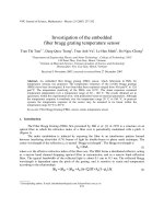
3. System testing
The dependence of the dc-output voltage from a PSD on the phase shift between the signal and the
reference (
θ
s
-
θ
r
)
The development of the output voltage X = V
s
sin(θ
s
-θ
r
) according to the phase shift between the
signal and the reference (θ
s
-θ
r
) in the first PSD is given in Fig.4. The same is for the output voltage
from the second PSD (Fig.5).
Fig. 4. Output voltage X vs. phase shift.
Fig. 5. Output voltage Y vs. phase shift.
The dependence of the dc-output voltage on frequency
Let have the reference at frequency 1kHz and the
effective signal V
o
= 1V. The frequency of the signal is
modulating from 980 Hz to 1020 Hz. The development
of the dc-output voltage (R) of a PSD according to the
frequency is given in Fig.6
This figure shows the maximal output voltage at
the frequency exactly equal to the reference frequency
(1000 Hz). There are also three different smaller
amplitudes. This shows the improvement of the lock-in
amplifier: it amplifies only the signal having the same
frequency as the reference signal whereas the other
signals are filtered off. In brief, the lock-in amplifier has an ability to suppress the noise belonging to
different frequencies than the reference.
Amplitude(V)
Phase shift (degree)
Phase shift (degree)
Amplitude(V)
Fig. 6. Output voltage vs. frequency.
Amplitude(V)
Frequency (Hz)
P.Q. Trieu, N.A. Duc / VNU Journal of Science, Mathematics - Physics 24 (2008) 239-244
243
The development of the amplitude and the phase shift according to the noise level
Let the reference frequency equal 1 kHz, the
maximal amplitude V
r
= 1 V. The measured signal
has the same frequency, and shifted in phase ϕ in
comparison to the reference. Let the amplitude of
the signal without noise is V
s
= 0.495 V. After the
incorporation of noise (white noise), the maximal
amplitude of the noise is 2.5 V, we received the
signal of the form showed in Fig.7. To continue this
test, we mix the signal with the increasing noise and
record the output voltage.
The result is showed in Fig.8. The Fig. 8 shows
the constancy of the output dc-voltage (V
s
= 0.495 V) when the amplitude of noise reaches 5V.
Similarly, we record the dependence of the phase shift on the amplitude of noise in Fig.9. If we take
the average of the measured data, we can obtain the more accurate result.
Fig. 8. The dependence of the output dc-voltage on
the noise level.
Fig. 9. The dependence of the phase shift on the noise
level.
4. Conclusion
The implemented two-phase lock-in amplifier is low-cost because it uses only one PC with
network card and a sound card with the pre-amplifier. It is easy to implement this device in the
laboratories. Its functionality is adaptible for very low level signal. The design characteristics can be
easily modified for various kinds of experiments. The data processing is automatic and convenient and
can be saved directly to disks. The further important application is that it can be used as a teaching
tool. Since the system uses Labview, it is easy to control and to evaluate the signals at every its
segments so provides clarity for users to understand the working of the digital lock-in amplifier.
Amplitude(V)
Phase(degree)
Noise (V)
Noise (V)
Fig. 7. Signal plus noise (maximal noise level 2.5V).
Amplitude(V)
P.Q. Trieu, N.A. Duc / VNU Journal of Science, Mathematics - Physics 24 (2008) 239-244
244
References
[1] Philip Kromer, Ralph Robinett, Roger Bengtson, Charles Hays, PC-Based Digital Lock-In Detection of Small Signals in
the Presence of Noise, Department of Physics, University of Texas at Austin,
[2] M.L. Meade, Lock-in amplifiers: Principles and Applications, Peter Peregrinus Ltd., London UK (1983).
[3] The Digital Lock-in Amplifier Technical Note TN1003, PerkinElmer Instruments Inc. 2000
[4] LIA-150 Dual Phase Lock-in Amplifier, Becker & Hickl GmbH Nahmitzer Damm Berlin (1999).
[5] MODEL SR830 DSP Lock-In Amplifier, Stanford Research Systems Inc (R2.2 2005).
[6] NI Lock-in Amplifier Start-Up Kit User Manual, National Instruments (8-2002).
[7] UTiLIA: A PC-Based Lock-in Amplifier (Using Labview), At
[8] Coly L. Crark, Labview Digital Processing and Digital Communications, McGraw-Hill Publisher (2005).
[9] Labview Measurement Manual, National Instruments Corporation Part Number 322661A-01 (2000 Edition).