high transmission nanoscale bowtie shaped aperture probe for near field
Bạn đang xem bản rút gọn của tài liệu. Xem và tải ngay bản đầy đủ của tài liệu tại đây (222.53 KB, 3 trang )
High transmission nanoscale bowtie-shaped aperture probe for near-field
optical imaging
Liang Wang and Xianfan Xu
a͒
School of Mechanical Engineering, Purdue University, West Lafayette, Indiana 47907
͑Received 12 March 2007; accepted 5 June 2007; published online 25 June 2007͒
A near-field scanning optical microscope probe integrated with nanoscale bowtie aperture for
enhanced optical transmission is demonstrated. The bowtie-shape aperture allows a propagating
mode in the bowtie gap region, which enables simultaneous nanoscale optical resolution and
enhanced optical transmission. The optical characteristics of the bowtie aperture are demonstrated
by measuring the optical near fields produced by the aperture. It is shown that bowtie aperture
probes have one order of magnitude increase in transmission over probes with a regular shape
aperture of the same resolution. The imaging results using bowtie aperture are in agreement with
those obtained from numerical calculations. © 2007 American Institute of Physics.
͓DOI: 10.1063/1.2752542͔
Since the demonstrations of the near-field scanning op-
tical microscope ͑NSOM͒ in 1984,
1,2
NSOM systems with
subwavelength resolution have become an important tool in
many application fields, including single molecule
detection,
3
nanofabrication,
4
and high density data storage.
5
The simplest way for obtaining nanoscale optical resolution
is to employ a nanoscale aperture in a metal screen.
6
Many
NSOMs use such a nanoscale aperture, called aperture-
NSOM, to achieve subwavelength resolution.
1,2
For aperture-
NSOMs, the size of the aperture at the apex of the probe
determines the ultimate optical resolution. Nowadays, ta-
pered optical fibers and microfabricated cantilever aperture
probes are commercially available, benefiting from the rapid
development of various fabrication techniques. The most
widely used aperture probe consists of a tapered optical fiber
obtained by heating and subsequent pulling to create an ap-
erture smaller than 100 nm.
1,2
Another method for manufac-
turing aperture NSOM probes is by wet chemical etching to
produce a taper with a sharp end point.
7,8
However, commer-
cial NSOM probes suffer from poor transmission efficiency
due to the wavelength cutoff effect, therefore light cannot be
efficiently coupled through.
9,10
To improve the optical transmission efficiency through
nanoscale apertures, a special type of nanoaperture in a
bowtie shape as well as its opposed part the bowtie antenna
has been investigated recently.
11–15
As shown in the top of
the left column in Fig. 1, a bowtie aperture has two open
arms and a gap. Numerical
11,12
and experimental studies
16,17
have demonstrated that the bowtie aperture allows propagat-
ing waveguide mode in the gap region under properly polar-
ized irradiation, which enables bowtie nanoapertures to si-
multaneously achieve nanoscale light concentration and
enhanced optical transmission. It is also known that surface
plasmon can enhance field transmission in noble metals. The
difference of using the bowtie aperture is that it provides a
broad band ͑from IR to UV͒ field localization and enhance-
ment and does not need to use noble metal which can be soft
͑gold͒ or unstable in air ͑silver͒. There is also plasmonic
effect in a bowtie aperture as studied in our earlier work,
11
which found that the plasmonic effect does not always local-
ize the field since the plasmon is a surface wave which
propagates along the surface and spreads the field.
As a high precision fabrication technique, focused ion
beam ͑FIB͒ milling has been used for fabricating subwave-
length aperture at a fiber tip and cantilever tip.
18,19
Here we
investigate fabricating bowtie aperture on NSOM probe to
utilize its superior optical characteristics. The transmission
enhancement of bowtie apertures is demonstrated by com-
paring with comparable square apertures by far-field mea-
surements. We then examine NSOM probes with nanoscale
bowtie apertures fabricated at the probe apex by FIB machin-
ing. The capability of bowtie aperture probes for optical im-
aging is demonstrated by comparing with regular aperture
probes using a homebuilt transmission-collection NSOM
system. The experimental results are also compared with nu-
merical simulations.
The bowtie apertures were fabricated using FIB milling.
A 150-nm-thick aluminum film was deposited on a quartz
a͒
Author to whom correspondence should be addressed; electronic mail:
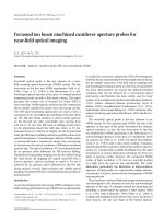
FIG. 1. ͑Color online͒ Left: scanning electron microscopy images of fabri-
cated bowtie and comparable square apertures. From top to bottom: bowtie
aperture with outline dimension of 160 nm, 105ϫ 105 nm
2
square aperture,
33ϫ33 nm
2
square aperture, bowtie aperture with outline dimension of
180 nm, and 130ϫ 130 nm
2
square aperture. Right: far-field transmission
measurement results of bowtie apertures and square apertures. The five im-
ages in each row are produced by five apertures of the same geometry to
show the consistency of the measurements.
APPLIED PHYSICS LETTERS 90, 261105 ͑2007͒
0003-6951/2007/90͑26͒/261105/3/$23.00 © 2007 American Institute of Physics90, 261105-1
Downloaded 27 Jun 2007 to 128.46.184.20. Redistribution subject to AIP license or copyright, see />wafer by e-beam deposition. Bowtie apertures with outline
dimensions of 160 and 180 nm and a gap of 33 nm were
fabricated. For the purpose of comparison, square apertures
with dimensions of 105ϫ105 nm
2
and 130ϫ130 nm
2
, hav-
ing the same opening area as the two bowtie apertures, and a
33ϫ33 nm
2
square aperture having the same area as the gap
of the bowtie aperture were fabricated ͑left column of Fig.
1͒. Transmission of the apertures was measured using a
458 nm argon ion laser. The transmitted laser light through a
single aperture in the sample is collected by a 50ϫ objective
lens and directed onto a photomultiplier tube ͑PMT͒. The
sample was raster scanned and recorded by the PMT signal
readout. The power throughput of each aperture can there-
fore be compared by the photon counts. The two bowtie
apertures with outline dimensions of 160 and 180 nm had
100ϫ10
3
and 160ϫ 10
3
/s photon counts, respectively. On
the other hand, there were only 5 ϫ 10
3
and 15ϫ10
3
/s pho-
ton counts obtained from the two comparable square aper-
tures. This indicates more than one order of magnitude
higher transmission from bowtie apertures when compared to
the square apertures with the same opening areas. The small
33ϫ33 nm
2
square apertures did not transmit enough light
to be detected by the PMT.
We then investigated using bowtie aperture on NSOM
probes and compared them with regular aperture probes. The
probe fabrication procedure is as follows. We started with
standard silicon nitride cantilevered atomic force microscopy
͑AFM͒ probes, which had a pyramidal-shaped tip near the
end of cantilever. On the tip of the probe, a platform was
created by FIB side slicing. Then an aluminum film of about
100 nm thick was deposited to cover the entire tip side of the
cantilever, including the platform. FIB drilling was then used
to make bowtie apertures and regular square apertures
through the aluminum film. The bowtie aperture fabricated
on the NSOM probe has a 180 nm outline dimension with a
33 nm gap. Figure 2 shows the front and side views of a
fabricated bowtie aperture probe.
The bowtie aperture probes were investigated using a
homebuilt transmission-collection NSOM system. The
sample was illuminated by an argon ion laser at a wavelength
of 458 nm. The transmitted light through the apertures on the
sample was collected by the NSOM probe and directed onto
a PMT. A 75
m pinhole was placed in the image plane of
the objective lens to block the ambient light. Standard AFM
feedback scheme based on light deflection was used to con-
trol the probe position. NSOM images were obtained by ras-
ter scanning the sample using a high precision piezoscanner
and recording the optical signal from the PMT by photon
counting.
We first characterized the probes by measuring light out-
put from 90ϫ90 nm
2
square apertures in aluminum film
͑coated on a quartz substrate͒. The full width at half maxi-
mum ͑FWHM͒ of the measured light spot is 110 nm, slightly
larger than the size of the aperture due to the convolution
between the aperture and finite size of the bowtie aperture on
the probe. To better characterize the optical resolution of
NSOM probes, a smaller or pointlike light source is needed.
One can obtain a smaller output light spot from an aperture
by reducing its size. However, the optical transmission
through subwavelength square aperture decreases drastically
as the aperture size is reduced. We have attempted measuring
a40ϫ 40 nm
2
square aperture but no signal was detected. On
the other hand, a bowtie aperture can also be used to produce
a small light spot with much higher transmission efficiency.
We characterized bowtie aperture probes by scanning
them over bowtie apertures made in aluminum film. For
comparison, square aperture probes with an opening of
90ϫ90 nm
2
were also used.
Figures 3͑a͒ and 3͑b͒ show the NSOM images obtained
by the bowtie aperture probe and the square aperture probe
using the same intensity scale. It was found that the bowtie
aperture probe provides near-field measurement counts seven
times higher than the regular aperture probe. Line scans of
the image shown in Figs. 3͑a͒ and 3͑b͒ are shown in Fig.
3͑c͒. The edge resolutions for both probes measured by
10%–90% criterion of the transmission power are about
90 nm. When using a bowtie aperture probe, a small amount
of light can transmit through the arm region of the bowtie
aperture. In the NSOM image, two tails were found at the
bottom of the scanning profile, as indicated in Fig. 3͑c͒,
which were possibly caused by the light leaking through the
arm regions of the bowtie aperture. It is also noted from Fig.
FIG. 2. Front and side views of a bowtie aperture probe. The bowtie aper-
ture has a 180 nm outline dimension and a 33 nm gap.
FIG. 3. ͑Color online͒ NSOM images obtained by ͑a͒ bowtie aperture probe
and ͑b͒ regular aperture probe. ͑c͒ Near-field line profiles of the two NSOM
images, and the solid line and dashed line represent bowtie and squarer
aperture probes, respectively.
261105-2 L. Wang and X. Xu Appl. Phys. Lett. 90, 261105 ͑2007͒
Downloaded 27 Jun 2007 to 128.46.184.20. Redistribution subject to AIP license or copyright, see />3 that compared with the one obtained using the square ap-
erture probe, the scanning profile obtained using the bowtie
aperture probe is different, which has a narrow peak in the
middle with a FWHM equal to 66 nm. ͑A dashed line is
drawn across the bottom of the narrow peak.͒ The FWHM of
the peak roughly equals the sum of the two gaps of the two
bowtie apertures, which can be explained by the enhanced
field in the gap region of the bowtie aperture.
The NSOM images obtained using a bowtie aperture
probe were also analyzed using finite difference time domain
͑FDTD͒ simulations, which have been previously used to
analyze other NSOM imaging processes.
20,21
Commercial
software package
XFDTD 5.3 from Remcom is used in this
work. 4ϫ4ϫ4nm
3
cells are used to model bowtie nanoap-
ertures. 1400 time steps were run which is determined ac-
cording to the stability criteria of the FDTD. Debye model
parameters of aluminum at 458 nm are found as
ϰ
=1,
s
=−507.825,
=9.398ϫ10
−16
s, and
=4.8ϫ10
6
s/m. The
simulation geometry includes two 150-nm-thick aluminum
layers in contact, with the bottom layer represents the aper-
ture sample. The top layer represents the bowtie probe, con-
sisting of a 180 nm outline bowtie aperture in aluminum fol-
lowed by a semi-infinite Si
3
N
4
layer. Plane wave of
wavelength of 458 nm polarized in the direction across the
bowtie gap irradiated the sample from the quartz substrate
side. In order to simulate the scanning process, the top layer
was moved by steps of 8 nm with respect to the bottom
layer. Both electric and magnetic components of the trans-
mitted filed were calculated and used to compute the Poyn-
ting vectors. Total transmitted power through the bowtie ap-
erture probe was then calculated by integrating the Poynting
vectors over the opening cross section of bowtie aperture.
Figure 4 plots the power throughput, which is calculated by
normalizing the transmitted power to the incident power of
the same area. Compared with Fig. 3͑c͒, it can be seen that
the calculated near-field image has a similar field distribution
with that obtained from NSOM measurement. The calculated
edge resolution using the 10%–90% transmission criterion is
84 nm. There is also a narrow peak in the middle of the
profile with a FWHM equal to 64 nm. These values match
the NSOM results very well.
In summary, we developed NSOM probes with inte-
grated bowtie apertures for enhancing optical transmission in
NSOM measurements. Far field measurement results demon-
strated that bowtie apertures provided transmitted field inten-
sity one order of magnitude higher than comparable regu-
larly shaped apertures. To characterize the optical resolution
of bowtie aperture probes, NSOM measurements using aper-
ture probe were carried out. It was found that the bowtie
aperture probe provides high optical transmission compared
with a probe with regular shaped aperture. The edge resolu-
tion of bowtie aperture probe was larger than the gap size of
the bowtie due to the light leaking through the arm. FDTD
numerical simulations were carried out and the results
matched with experimental findings. This work demonstrated
unique properties of bowtie aperture probes compared with
regular NSOM probes.
The financial support to this work by the National Sci-
ence Foundation is acknowledged. Fabrications of aperture
samples and NSOM probes by FIB were carried out in the
Birck Nanotechnology Center, Purdue University.
1
D. W. Pohl, W. Denk, and M. Lanz, Appl. Phys. Lett. 44,651͑1984͒.
2
A. Lewis, M. Isaacson, A. Harootunian, and A. Muray, Ultramicroscopy
13, 227 ͑1984͒.
3
E. Betzig and R. J. Chichester, Science 262, 1422 ͑1993͒.
4
I. I. Smolyaninov, D. L. Mazzoni, and C. C. Davis, Appl. Phys. Lett. 67,
3859 ͑1995͒.
5
E. Betzig, J. K. Trautman, R. Wolfe, E. M. Gyorgy, P. L. Finn, M. H.
Kryder, and C. H. Chang, Appl. Phys. Lett. 61, 142 ͑1992͒.
6
E. H. Synge, Philos. Mag. 6, 356 ͑1928͒.
7
P. Hoffmann, B. Dutoit, and R. Salathé, Ultramicroscopy 61,165͑1995͒.
8
D. Zeisel, S. Nettesheim, B. Dutoit, and R. Zenobi, Ultramicroscopy 68,
2491 ͑1996͒.
9
H. Bethe, Phys. Rev. 66, 163 ͑1944͒.
10
G. A. Valaskovic, M. Holton, and G. H. Morrison, Appl. Opt. 34, 1215
͑1995͒.
11
E. X. Jin and X. Xu, Appl. Phys. Lett. 86, 111106 ͑2005͒.
12
K. Sendur and W. Challener, J. Microsc. 210, 279 ͑2002͒.
13
R. Grober, R. Schoelkopf, and D. Prober, Appl. Phys. Lett. 70, 1354
͑1997͒.
14
W. Challener, T. Mcdaniel, C. Mihalcea, K. Mountfield, K. Pelhos, and I.
Sendur, Jpn. J. Appl. Phys., Part 1 42, 981 ͑2003͒.
15
W. Challener, E. Gate, A. Itagi, and C. Peng, Jpn. J. Appl. Phys., Part 1
45, 6632 ͑2006͒.
16
L. Wang, S. M. Uppuluri, E. X. Jin, and X. Xu, Nano Lett. 6,361͑2006͒.
17
E. X. Jin and X. Xu, Appl. Phys. Lett. 88,153110͑2006͒.
18
J. A. Veerman, A. M. Otter, L. Kuipers, and N. F. Van Hulst, Appl. Phys.
Lett. 72,3115͑1998͒.
19
Y. Mitsuoka, T. Niwa, S. Ichihara, K. Kato, H. Muramatsu, K. Nakajima,
M. Shikida, and K. Sato, J. Microsc. 202,12͑2001͒.
20
O. Martin, J. Microsc. 194, 235 ͑1999͒.
21
M. Spajer, G. Parent, C. Bainier, and D. Charraut, J. Microsc. 202,45
͑2001͒.
FIG. 4. Scanning profile obtained from the simulation results.
261105-3 L. Wang and X. Xu Appl. Phys. Lett. 90, 261105 ͑2007͒
Downloaded 27 Jun 2007 to 128.46.184.20. Redistribution subject to AIP license or copyright, see />