highly efficient blue organic light emitting diodes using quantum well like
Bạn đang xem bản rút gọn của tài liệu. Xem và tải ngay bản đầy đủ của tài liệu tại đây (2.23 MB, 16 trang )
Nanoscale Research Letters
This Provisional PDF corresponds to the article as it appeared upon acceptance. Fully formatted
PDF and full text (HTML) versions will be made available soon.
Highly efficient blue organic light-emitting diodes using quantum well-like
multiple emissive layer structure
Nanoscale Research Letters 2014, 9:191
doi:10.1186/1556-276X-9-191
Ju-An Yoon ()
You-Hyun Kim ()
Nam Ho Kim ()
Seung Il Yoo ()
Sang Youn Lee ()
Fu Rong Zhu ()
Woo Young Kim ()
ISSN
1556-276X
Article type
Nano Idea
Submission date
7 February 2014
Acceptance date
2 April 2014
Publication date
24 April 2014
Article URL
/>
This peer-reviewed article can be downloaded, printed and distributed freely for any purposes (see
copyright notice below).
Articles in Nanoscale Research Letters are listed in PubMed and archived at PubMed Central.
For information about publishing your research in Nanoscale Research Letters go to
/>For information about other SpringerOpen publications go to
© 2014 Yoon et al.
This is an Open Access article distributed under the terms of the Creative Commons Attribution License ( which
permits unrestricted use, distribution, and reproduction in any medium, provided the original work is properly credited.
Highly efficient blue organic light-emitting diodes
using quantum well-like multiple emissive layer
structure
Ju-An Yoon1
Email:
You-Hyun Kim1
Email:
Nam Ho Kim1
Email:
Seung Il Yoo1
Email:
Sang Youn Lee1
Email:
Fu Rong Zhu2
Email:
Woo Young Kim1*
*
Corresponding author
Email:
1
Department of Green Energy & Semiconductor Engineering, Hoseo University,
Asan 336-795, South Korea
2
Department of Physics, Hong Kong Baptist University, Hong Kong, China
Abstract
In this study, the properties of blue organic light-emitting diodes (OLEDs), employing
quantum well-like structure (QWS) that includes four different blue emissive materials of
4,4′-bis(2,2′-diphenylyinyl)-1,1′-biphenyl (DPVBi), 9,10-di(naphth-2-yl)anthracene (ADN),
2-(N,N-diphenyl-amino)-6-[4-(N,N-diphenyl amine)styryl]naphthalene (DPASN), and bis(2methyl-8-quinolinolate)-4-(phenyl phenolato) aluminum (BAlq), were investigated.
Conventional QWS blue OLEDs composed of multiple emissive layers and charge blocking
layer with lower highest occupied molecular orbital (HOMO)-lowest unoccupied molecular
orbital (LUMO) energy level, and devices with triple emissive layers for more significant
hole-electron recombination and a wider region for exciton generation were designed. The
properties of triple emissive layered blue OLEDs with the structure of indium tin oxide (ITO)
/N,N′-diphenyl-N,N′-bis(1-naphthyl-phenyl)-(1,1′-biphenyl)-4,4′-diamine (NPB) (700 Ǻ)/X
(100 Ǻ)/BAlq (100 Ǻ)/X (100 Ǻ)/4,7-diphenyl-1,10-phenanthroline (Bphen) (300 Ǻ)/lithium
quinolate (Liq) (20 Ǻ)/aluminum (Al) (1,200 Ǻ) (X = DPVBi, ADN, DPASN) were
examined. HOMO-LUMO energy levels of DPVBi, ADN, DPASN, and BAlq are 2.8 to 5.9,
2.6 to 5.6, 2.3 to 5.2, and 2.9 to 5.9 eV, respectively. The OLEDs with
DPASN/BAlq/DPASN QWS with maximum luminous efficiency of 5.32 cd/A was achieved
at 3.5 V.
Keywords
Blue organic light-emitting diodes; HOMO-LUMO; QWS
Background
Since the report by Tang and VanSlyke on organic light-emitting diodes (OLEDs), [1,2]
OLEDs have become a popular research subject due to its several technical advantages such
as reduced power consumption, compatibility with flexible substrates, high color rendering
index, high contrast, and wide viewing angle. OLEDs have emerged as strong candidates for
next-generation flat panel displays and solid-state lighting sources [3-6]. Many progresses
have been made in improving the performance of OLEDs, including high power efficiency
tandem organic light-emitting diodes based on bulk heterojunction organic bipolar charge
generation layer [7]. However, improving the performance of blue OLEDs still remains as an
open challenge [8-10]. Various methods have been developed to optimize blue OLED's
performance. Such methods include replacing emitters from fluorescent to phosphorescent
materials [11], including balancing the carrier ratio in the emissive layer (EML) [12],
designing a better surface texture for improving external quantum efficiency [13], and
reduced efficiency roll-off in OLEDs at ultrahigh current densities by suppression of tripletpolaron quenching [14].
Among various methods for enhanced efficiency, the QWS has proved to be an effective
approach for high device performance [15,16], by confining charge carriers and exciton
within the multi-emitting layer. Thus, the charge carrier recombination efficiency and exciton
formation probability can be beneficially enhanced [17]. The organic molecules were
insufficiently restricted by Van der Waals force among molecules in the organic quantum
well. The main features of QWS were high electroluminescence (EL) efficiency [18], tunable
EL zone [19], and great carrier balance [20-23].
In this study, the performance of blue OLEDs with multiple emissive layers 4,4′-bis(2,2′diphenylyinyl)-1,1′-biphenyl (DPVBi), 9,10-di(naphth-2-yl)anthracene (ADN), 2-(N,Ndiphenyl-amino)-6-[4-(N,N-diphenyl amine)styryl]naphthalene (DPASN), and bis(2-methyl8-quinolinolate)-4-(phenyl phenolato) aluminum (BAlq) was investigated. These emissive
materials have different highest occupied molecular orbital (HOMO)-lowest unoccupied
molecular orbital (LUMO) energy levels. Emissive layers with different orders in the QWStype OLEDs were investigated and optimized to achieve the best device performances.
Luminous efficiency and I-V-L characteristics were observed considering the effects of QWS
and the variation of recombination region in EML.
Experiment
Indium tin oxide (ITO)-coated glass was cleaned in ultrasonic bath by regular sequences: in
acetone, methanol, diluted water, and isopropyl alcohol. Hereafter, pre-cleaned ITO was
treated by O2 plasma under condition of 2 × 10⁻² Torr and 125 W for 2 min. Blue OLEDs
were fabricated using the high vacuum (1.0 × 10⁻⁶ Torr) thermal evaporation and N,N′-
diphenyl-N,N′-bis(1-naphthyl-phenyl)-(1,1′-biphenyl)-4,4′-diamine (NPB), BAlq, DPVBi,
ADN, DPASN, 4,7-diphenyl-1,10-phenanthroline (Bphen), lithium quinolate (Liq), and
aluminum (Al) were deposited at different evaporation rates of 1.0, 0.5, 0.5, 0.5, 0.5, 1.0, 0.1,
5.0 Ǻ/s.
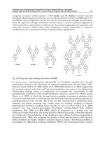
Figure 1 shows the molecular structures of the different blue chromophores used in the
OLED devices. We fabricated two types of blue OLEDs. The first type has a conventional
device structure of ITO/NPB/DPVBi or ADN or DPASN/BAlq/Bphen/Liq/Al, where ITO,
NPB, DPVBi (or ADN or DPASN), and Al are the anode, hole transporting layer, emissive
layer, electron transporting layer, and cathode, respectively. The other type of blue OLEDs
with a structure of ITO/NPB/DPVBi or ADN or DPASN/BAlq/DPVBi or ADN or
DPASN/Bphen/Liq/Al was also fabricated for comparison studies. A list of OLEDs with
different layer structures is summarized in Table 1.
Figure 1 Molecular structures of different blue emissive materials used in this work.
Table 1 Layer structures of OLED devices A, B, C, and D
Structure
Device A
ITO (1,800 Ǻ)/NPB (700 Ǻ)/DPVBi (300 Ǻ)/Bphen (300 Ǻ)/Liq (20 Ǻ)/Al
(1,200 Ǻ)
Device B
ITO (1,800 Ǻ)/NPB (700 Ǻ)/ADN (300 Ǻ)/Bphen (300 Ǻ)/Liq (20 Ǻ)/Al
(1,200 Å)
Device C
ITO (1,800 Ǻ)/NPB (700 Ǻ)/DPASN (300 Ǻ)/Bphen (300 Ǻ)/Liq (20 Ǻ)/Al
(1,200 Ǻ)
Device D
ITO (1,800 Ǻ)/NPB (700 Ǻ)/BAlq (300 Ǻ)/Bphen (300 Ǻ)/Liq (20 Ǻ)/Al
(1,200 Ǻ)
Device E
ITO (1,800 Ǻ)/NPB (700 Ǻ)/DPVBi (100 Ǻ)/BAlq (100 Ǻ)/DPVBi (100
Ǻ)/Bphen (300 Ǻ)/Liq (20 Ǻ)/Al (1,200 Ǻ)
Device F
ITO (1,800 Ǻ)/NPB (700 Ǻ)/ADN (100 Ǻ)/BAlq (100 Ǻ)/ADN (100 Ǻ)/Bphen
(300 Ǻ)/Liq (20 Ǻ)/Al (1,200 Ǻ)
Device G
ITO (1,800 Ǻ)/NPB (700 Ǻ)/DPASN (100 Ǻ)/BAlq (100 Ǻ)/DPASN (100
Ǻ)/Bphen (300 Ǻ)/Liq (20 Ǻ)/Al (1,200 Ǻ)
With various DC voltage bias, the optical and electrical properties of blue OLEDs such as the
current density, luminance, power efficiency, luminous efficiency, Commission
Internationale deL'eclairage (CIExy) coordinates, and electroluminescence spectra were
measured with Keithley 238 (Seoul, Korea), LMS PR-650 spectrophotometer and colorimeter
(Photo Research Inc., CA, USA) and the IVL system (LMS Inc., Gyeonggi-do, Korea).
Results and discussion
Figure 2a shows the current density-voltage characteristics measured for each conventional
blue OLED devices. Device C has the highest current density, and its EML consists of
DPASN which is a p-type emitting material with a higher hole mobility; device B, which also
had a p-type material, shows the second highest current density device. However, device D
with an n-type emitting material of BAlq shows the lowest current density. Consequently, we
realized that a p-type semiconductor has more electron affinity than a n-type semiconductor
[24]. Figure 2b shows the current density-voltage characteristics measured for each QWS
triple emissive layer blue OLED device. Devices E, F, and G actually have similar current
density characteristic, and this phenomenon is caused by different charge injection barriers
between emitting materials. The energy band diagrams of devices A to G are shown in Figure
3. Although it is not so significant to compare other QWS blue OLED devices, the device G
including DPASN shows the highest current density at 8 V because the hole and electron
injection barriers of device G were higher than those of another devices. As a result, the
charge flow of charge injection barriers are interrupted, in turn decreasing its current density.
Current densities of QWS blue OLED devices E, F, and G were lower than that of
conventional OLED devices A, B, and C because electrons and holes are confined in the
QWS which could possibly inhibit the current flow in EML.
Figure 2 Current density-voltage characteristics. Measured for (a) conventional blue
OLED devices A, B, C, and D and (b) OLEDs E, F, and G with QWS multiple emissive
layers.
Figure 3 HOMO-LUMO energy levels of the functional organic materials used in the
device fabrication.
Figure 4a,b shows the luminance-voltage (L-V) characteristics of conventional blue OLEDs
and QWS multi-emissive layer blue OLEDs. Conventional blue OLEDs have higher
luminance than QWS blue OLEDs. This is because QWS blue OLEDs consist of p-type
emissive materials of DPVBi, ADN, and DPASN, and n-type emissive material of BAlq
together. Consequently, n-type emissive materials influence on luminance much more than ptype emissive material although p-type emissive materials tend to have a higher luminance
characteristic. Table 2 summarizes the luminance of each blue OLED device measured at 5,
6, and 7 V.
Figure 4 Luminance-voltage characteristics. (a) Conventional OLED devices A, B, C, and
D and (b) QWS OLED devices E, F, and G.
Table 2 Luminance of OLED devices measured at 5 to 7 V
5V
6V
2
Device A
432.5 cd/m
1,461 cd/m2
2
Device B
431.3 cd/m
1,384 cd/m2
Device C
1,296 cd/m2
3,071 cd/m2
Device D
89.17 cd/m2
538.6 cd/m2
1,083 cd/m2
Device E
291.6 cd/m2
Device F
216.9 cd/m2
801.1 cd/m2
2
Device G
454.9 cd/m
1,489 cd/m2
7V
3,777 cd/m2
3,460 cd/m2
4,750 cd/m2
1,840 cd/m2
2,925 cd/m2
2,192 cd/m2
3,696 cd/m2
Figure 5a,b shows the plot of luminous efficiency versus current density of conventional blue
OLED device and QWS multi-emissive blue OLED devices. Table 3 summarizes the
luminous efficiency of each device ranging from 50 to 150 mA/cm2. Luminous efficiency of
QWS blue OLED devices is higher than that of conventional OLED devices. This
phenomenon caused by emissive region of QWS OLED was evenly formed by DPVBi,
ADN, DPASN, and BAlq. As a result, the power efficiency was enhanced because ADN and
BAlq were emissive at different wavelengths. However, devices including DPASN show
remarkable enhancement of efficiency. This can be explained by depth of QWS according to
the difference of HOMO-LUMO energy level of emissive materials. HOMO and LUMO
difference of DPVBi, BAlq, AND, and BAlq was 0, 0.1, 0.3, and 0.3 eV, respectively. This
HOMO and LUMO level difference is not enough to confine charges and excitons in the
emissive layer. Therefore, it was not enough to enhance luminous efficiency of OLED
devices. However, when DPASN was used, luminous efficiency remarkably improved
because HOMO and LUMO level difference of QWS OLED device was 0.7 and 0.6 eV
between DPASN and BAlq. Therefore, QWS OLED devices need enough intermolecular
HOMO and LUMO level difference of more than at least 0.3 eV.
Figure 5 Luminous efficiencies. (a) Conventional OLED devices A, B, C, and D and (b)
QWS OLED devices E, F, and G as a function of the current density.
Table 3 Luminous efficiency of OLED devices measured at different current densities of
50 to 150 mA/cm2
50 mA/cm2
100 mA/cm2
150 mA/cm2
Device A
3.01 cd/A
2.86 cd/A
2.57 cd/A
Device B
2.48 cd/A
2.19 cd/A
2.14 cd/A
Device C
2.93 cd/A
2.65 cd/A
2.31 cd/A
Device D
3.62 cd/A
3.38 cd/A
3.31 cd/A
Device E
3.24 cd/A
2.85 cd/A
2.84 cd/A
Device F
2.62 cd/A
2.23 cd/A
2.21 cd/A
Device G
3.97 cd/A
3.64 cd/A
3.60 cd/A
The depth of QWS according to the difference of HOMO-LUMO energy level of emissive
materials was concerned with the performance of the OLED. It is shown that the performance
of OLEDs changes according to the depth of QWS (Figure 6). Figure 6 shows the plot of
external quantum efficiency (EQE) as a function of current density for conventional OLEDs
and QWS OLEDs. EQEs of OLED devices measured at 100 mA/cm2 were 2.71%, 2.21%,
1.99%, 1.75%, 2.53%, 1.81%, and 2.76%, respectively. QWS OLEDs having DPASN
demonstrated a 38% enhancement in EQE. However, if QWS OLED devices include ADN
and DPVBi, the EQE did not change or decrease. As mentioned before, when using DPASN,
EQE enhances because the depth of QWS OLED device is enough for 0.7 and 0.6 eV. If
QWS OLED devices include ADN and DPVBi, the depth of QWS was not enough to
enhance EQE, and the emission region was formed at BAlq with lower EQE. Therefore, the
EQE of OLED devices was decreased.
Figure 6 External quantum efficiency-current density characteristics measured for
conventional OLEDs and QWS OLEDs.
Figure 7 shows the EL spectra of conventional OLED devices and QWS OLED devices at 5
V. We know that if QWS OLED devices include ADN and DPVBi, the full width at half
maximum (FWHM) of EL spectra was increased. We can observe this result in Figure 7a,b.
As the result demonstrates, the emission region formed at BAlq. However, when using
DPASN at QWS OLED, the EL spectra remained almost the same.
Figure 7 A comparison of EL spectra measured for conventional OLEDs and QWS
OLEDs at 5 V (a, b).
Conclusions
Blue OLED with triple emissive layer structure achieved luminous efficiency of 5.23 cd/A at
3.5 V, which is 36% higher than that of the conventional blue OLEDs. Obviously, the
quantum well-like structure is favorable for hole-electron recombination for efficient exciton
generation in the multiple emissive layers of DPVBi, ADN, and DPASN with BAlq in the
device. There was no significant improvement in the luminous efficiency (only about 3% and
4%) when DPVBi and ADN were used as the additional emitting layer to form a quantum
well-like structure; a 36% improvement in luminous efficiency was realized in
DPASN/BAlg/DPASN blue OLEDs. This result shows that blue OLEDs can only improve
luminous efficiency under proper difference in HOMO and LUMO energy level between the
central and surrounding emitting layers. The effect of layer thickness and combination of
different emissive layers on charge carrier transport mechanism from the quantum well-like
and the blue emitting layer based on space charge limited current will be further examined.
Competing interests
The authors declare that they have no competing interests.
Authors’ contributions
JY and YK conceived and designed the experiments. JY and NHK carried out the
experiments with contributions from SYL. FRZ designed and synthesized the materials of
OLEDs. SIY carried out the characterization of devices. YK supervised the work. JY and
WYK wrote the manuscript. All authors read and approved the final manuscript.
Acknowledgements
This work was supported by the Nano-Convergence Foundation (Project Number: B0030016) funded by the Ministry of Education, Science and Technology (MEST, Korea) and
the Ministry of Knowledge Economy (MKE, Korea).
References
1. Tang CW, VanSlyke SA: Organic electroluminescent diodes. Appl Phys Lett 1987,
51:913.
2. Tatsuo M, Takaaki I, Teruyoshi Mizutani J: Electroluminescent properties of organic
light-emitting diodes with blue-emitting Alq. Photopolym Sci Technol 2004, 17:2.
3. Reineke S, Lindner F, Schwartz G, Seidler N, Walzer K, Lüssem B, Leo K: White organic
light-emitting diodes with fluorescent tube efficiency. Nature 2009, 59:234.
4. Gu G, Burrows PE, Venkatesh S, Forrest SR, Thompson ME: Vaccum-deposited,
nonpolymeric flexible organic light-emitting devices. Opt Lett 1997, 22:172.
5. Dandan S, Suling Z, Hany A: Modification of exciton lifetime by the metal cathode in
phosphorescent OLEDs, and implications on device efficiency and efficiency roll-off
behavior. Adv Funct Mater 2011, 21:2311.
6. Choi WH, Tam HL, Zhu FR, Ma DG, Sasabe H, Kido J: High performance
semitransparent phosphorescent white organic light emitting diodes with bi-directional
and symmetrical illumination. Appl Phys Lett 2013, 102:153308.
7. Chen YH, Chen JS, Ma DG, Yan DH, Wang LX, Zhu FR: High power efficiency tandem
organic light-emitting diodes based on bulk heterojunction organic bipolar charge
generation layer. Appl Phys Lett 2011, 98:243309.
8. D'Andrade BW, Forrest SR: White organic light-emitting devices for solid-state
lighting. Adv Mater (Weinheim, Ger) 2004, 16:1585.
9. Krummacher BC, Choong VE, Mathai MK, Choulis SA, So F, Jermann F, Fiedler T,
Zachau M: Highly efficient white organic light-emitting diode. Appl Phys Lett 2006,
88:113506.
10. D'Andrade BW, Holmes RJ, Forrest SR: Efficient organic electrophosphorescent
white-light-emitting device with a triple doped emissive layer. Adv Mater (Weinheim,
Ger) 2004, 16:624.
11. Shinar J: Organic Light-Emitting Devices. New York: Springer; 2004.
12. Gautier-Thianche E, Sentein C, Lorin A, Denis C, Raimond P, Nunzi JM: Effect of
coumarin on blue light-emitting diodes based on carbazol polymers. J Appl Phys 1998,
83:4236.
13. Hubert C, Fiorini-Debuisschert C, Hassiaoui I, Rocha L, Raimond P, Nunzi JM:
Emission properties of an organic light-emitting diode patterned by a photoinduced
autostructuration process. Appl Phys Lett 2005, 87:191105.
14. Zang FX, Sum TC, Huan ACH, Li TL, Li WL, Zhu FR: Reduced efficiency roll-off in
phosphorescent organic light emitting diodes at ultrahigh current densities by
suppression of triplet-polaron quenching. Appl Phys Lett 2008, 93:023309.
15. Kim SH, Jang J, Hong JM, Lee JY: High efficiency phosphorescent organic light
emitting diodes using triplet quantum well structure. Appl Phys Lett 2007, 90:173501.
16. Liu SM, Li B, Zhang LM, Song H, Jiang H: Enhanced efficiency and reduced roll-off
in nondoped phosphorescent organic light-emitting devices with triplet multiple
quantum well structures. Appl Phys Lett 2010, 97:083304.
17. Zhao J, Junsheng Y, Zhang L, Wang J: Non-doped phosphorescent white organic lightemitting devices with a quadruple-quantum-well structure. Physica B 2012, 407:2753.
18. Ohmori Y, Fujii A, Uchida M, Morishima C, Yoshino K: Fabrication and
characteristics of 8‐hydroxyquinoline aluminum/aromatic diamine organic multiple
‐
quantum well and its use for electroluminescent diode. Appl Phys Lett 1993, 62:3250.
19. Qiu Y, Gao Y, Wang L, Wei P, Duan L, Zhang D, Dong G: High-efficiency organic
light-emitting diodes with tunable light emission by using aromatic diamine/5,6,11,12tetraphenylnaphthacene multiple quantum wells. Appl Phys Lett 2002, 81:3540.
20. Qiu Y, Gao Y, Wei P, Wang L: Organic light-emitting diodes with improved holeelectron balance by using copper phthalocyanine/aromatic diamine multiple quantum
wells. Appl Phys Lett 2002, 80:2628.
21. Song SF, Zhao DW, Xu Z, Xu XR: Energy transfer in organic quantum well
structures. Acta Phys Sin 2007, 56:3499.
22. Zhu HN, Xu Z, Zhao SL, Zhang FJ, Kong C, Yan G, Gong W: Influence of well
structure on efficiency of organic light-emitting diodes. Acta Phys Sin 2010, 59:8093.
23. Jian Z, Juan G, Zhuo G, Ke D, Jiule C: An organic light-emitting device with ultrathin
quantum-well structure as light emitting layer. Opt Rev 2011, 18:394.
24. Culligan W, Chen AC-A, Wallace JU, Klubek KP, Tang CW, Chen SH: Effect of hole
mobility through emissive layer on temporal stability of blue organic light-emitting
diodes. Adv Funct Mater 2006, 16:1481.
DPVBi
Figure 1
DPASN
ADN
BAlq
Figure 2
Figure 3
Figure 4
Figure 5
Figure 6
Figure 7