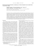
thermomechanical and thermal contact characteristics of bismuth telluride films electrodeposited on carbon nanotube arrays
Bạn đang xem bản rút gọn của tài liệu. Xem và tải ngay bản đầy đủ của tài liệu tại đây (286.69 KB, 4 trang )
Thermomechanical and Thermal Contact
Characteristics of Bismuth Telluride Films
Electrodeposited on Carbon Nanotube Arrays
By Himanshu Mishra, Baratunde A. Cola, Vijay Rawat, Placidus B. Amama,
Kalapi G. Biswas, Xianfan Xu, Timothy S. Fisher, and Timothy D. Sands*
A miniaturized thermoelectric (TE) cooler module is composed of
a large number of TE legs connected electrically in series and
thermally in parallel.
[1]
TE devices operating near room
temperature typically create a temperature difference of
30–50 8C, and the TE film thickness for such devices ranges
from 10 to 100mm.
[2]
From manufacturing and reliability
perspectives, the design of TE cooler modules is often
constrained by the shear stresses that result from differential
thermal expansion, both during steady-state operation and during
on/off cycling. In bulk systems, various strategies, such as
spring-loaded systems, tension bolts, and welding, have been
proposed to enhance compliance during device operation.
[3]
However, none of these strategies can be directly applied to
thin-film based miniaturized TE devices. Additionally, for TE
devices operating at higher temperatures, a pressing need exists
for stable, compliant, and low thermal resistance interface
materials between the TE element and the metallic interconnects.
With this motivation, we report here a scalable electrodeposition
process to integrate thick-film TE materials with carbon
nanotubes (CNT) arrays.
Recently, CNT arrays have been reported to exhibit excellent
fatigue strength under cyclic compressive loading
[4]
and as
interface materials, they have been shown to achieve low
thermal
[5]
and electrical
[6]
interface resistances at moderate
contact pressures. Further, CNTs are amenable to heterogeneous
integration with other materials.
[7]
These attributes suggest that
compliant CNT arrays can be integrated with minimal parasitic
additions to the total electrical and thermal resistances of a TE
device.
The common substrate for this work was 5 Â 6mm
2
Ni(200 nm)/Ti (800 m)/SiO
2
(1 mm)/Si(300 mm). For CNT array
synthesis, some of these substrates were coated with a metal
tri-layer structure of Fe (2.5nm)/Al(10 nm)/Ti(30 nm) by electro-
n-beam evaporation. Multi-walled CNT arrays were synthesized
on these substrates by microwave-plasma chemical vapor
deposition (MPCVD). The feed gases for the reaction were
methane at 10 standard cubic centimeter per minute (sccm), and
hydrogen at 50 sccm, The reaction temperature and pressure
were 1173 K and 10 Torr (1 Torr ¼ 133.32 Pa), respectively. Further
details of the CNT synthesis by the MPCVD technique have been
reported.
[5]
The remaining substrates, without CNTs, served as
control samples. CNTarrays were imaged using a Hitachi S-4800
field-emission scanning electron microscope (FESEM) (Fig. 1).
The average length and diameter of the CNTs were 25 mm and
40 nm, respectively.
Bismuth telluride (Bi
2
Te
3
) was chosen as a representative TE
material for TE/CNT integration by electrodeposition, as it is the
parent compound of the alloys used in commercial Peltier devices
optimized for cooling at temperatures near 300 K.
[8]
Using a
Bio-Analytical Systems (BAS) Epsilon Electrochemical System,
Bi
2
Te
3
was electrodeposited potentiostatically on the CNT
array-coated substrates, and these films were compared with
Bi
2
Te
3
films electrodeposited directly on bare metallized
substrates. A three-electrode setup was used with a CNT
array-coated working electrode, platinum mesh counter elec-
trode, and an Ag/AgCl (3
M NaCl, 0.175 V versus NHE) reference
electrode. The deposition bath was composed of Bi
3þ
(0.75 Â 10
À2
M) and HTeO
2
þ
(1 Â 10
À2
M) (both Alfa Aesar,
99.999% pure) and HNO
3
(1 M) at 298 K.
[2,9]
Continuous
one-minute pulses at À50 mV were applied between the working
and the reference electrodes for about 10 h for electrodeposition
COMMUNICATION
www.advmat.de
[*] Prof. T. D. Sands, V. Rawat, P. B. Amama, K. G. Biswas
School of Materials Engineering, Purdue University West Lafayette
IN 47907 (USA)
E-mail:
Prof. T. D. Sands, H. Mishra, B. A. Cola, V. Rawat, P. B. Amama, K. G.
Biswas, X. Xu, Prof. T. S. Fisher
Birck Nanotechnology Center 1205 West State Street, West Lafayette,
IN 49707-2057 (USA)
Prof. T. D. Sands
School of Electrical and Computer Engineering, Purdue University
West Lafayette, IN 47907 (USA)
H. Mishra, B. A. Cola, Prof. T. S. Fisher
School of Mechanical Engingeering, Purdue University West Lafay-
ette IN 47907 (USA)
DOI: 10.1002/adma.200803705
Figure 1. a) Side view of the MWCNT array and b) magnified image of
MWCNT array.
Adv. Mater. 2009, 21, 1–4 ß 2009 WILEY-VCH Verlag GmbH & Co. KGaA, Weinheim 1
COMMUNICATION
www.advmat.de
of $50 mm thick Bi
2
Te
3
films while maintaining a current density
of about 5 mA cm
À2
.
FESEM images were obtained to assess the morphology of the
deposited TE/CNT heterostructures in both plan and cross-
sectional views (Fig. 2a–c). It can be inferred from the FESEM
images that the Bi
2
Te
3
electrodeposited on and around the CNTs
and ultimately extended above the CNT array as a continuous
polycrystalline thin film. Different durations of electrodeposition
resulted in film thicknesses ranging from 1 to 100 mm. Figure 2d
shows X-ray diffraction patterns obtained from a Bi
2
Te
3
film
deposited directly on a silicon substrate and another grown on
CNT array. The X-ray diffraction patterns confirm the presence of
polycrystalline Bi
2
Te
3
film on the CNT array, and the crystalline
quality of the film is similar to that grown under similar
electrodeposition conditions directly on a metalized silicon
substrate. There is a detectable influence of the CNT array on the
orientation of the Bi
2
Te
3
film and that effect is observed in X-ray
diffraction patterns. Some of the X-ray diffraction peaks observed
in the pattern from the TE/M heterostructure were found to be
missing, or slightly displaced in the pattern from the TE/CNT/M
heterostructure (Fig. 2d). This is expected because the CNT array
underlayer, as opposed to the metal substrate, is a non-planar
substrate that is mechanically compliant. Thus, any influence of
the substrate on crystallographic texture or deposition-induced
stress will be manifested in subtle differences in peak intensity
and diffraction angle. The possibility that carbon contamination
from the CNTs could have influenced the texture and lattice
parameters is remote, as there was no evidence of CNT
dissolution during electrodeposition, and the
Bi
2
Te
3
were sufficiently thick to ensure that
much of the growth occurred by Bi
2
Te
3
deposition on Bi
2
Te
3
rather than on CNTs
directly.
For electrodeposition of Bi
2
Te
3
patterns on
CNT coated surfaces, towards development of
a multi-coupled TE device, an optical litho-
graphy-based fabrication process was devel-
oped. On a CNT array coated surface (CNT/Ni
(200 nm)/Ti (800 nm)/SiO
2
(1 mm)/Si
(300 mm)), MicroChemicals AZ-9260 was spin-
coated to obtain a photoresist layer with a
thickness of $7 mm. The photoresist was then
patterned using optical lithography to open
windows for the electrodeposition of Bi
2
Te
3
patterns. The underlying metallic layer
beneath the CNT layer provided an electrically
conducting path through the sample, and the
non-conducting photoresist mold restricted
electrodeposition of TE materials to the
exposed CNT region. This strategy may be
employed to develop p- and n-type TE legs on
CNT array coated metallic surfaces for thermo-
mechanically compliant multi-couple TE
microdevices (Fig. 3a, b).
To study the effects of the CNT interface
material on the relative thermomechanical
robustness of the TE/CNT/M heterostructure,
the temperature excursion required to induce
catastrophic failure (i.e., delamination of the
film) was assessed for samples with and without the CNT
interface material. The samples were compared to Bi
2
Te
3
films
(5 mm thickness) with lateral dimensions of 5 mm by 6 mm
deposited directly on either metallized (Ni(200 nm)/Ti(800 nm)/
SiO
2
(1 mm)/Si(300 mm)) substrates or 25 mm thick CNT arrays
grown on the same metallized substrate. Samples of both types
were subjected to the same thermal cycle (ramp ¼ 600 8Ch
À1
,
dwell ¼ 1 h, quench to room temperature) in forming gas (5% H
2
,
95% Ar) in a controlled environment furnace (Lindberg
horizontal, three zone tube furnace).
After each thermal cycle, the films were visually analyzed for
signs of cracks or peeling, and the observations are presented in
Table 1. For samples without a CNT interlayer, TE films
completely delaminated from the substrates for a temperature
rise (DT ¼ T
Furnace
À T
Room
) greater than 200 K. However, for the
Figure 2. FESEM images showing a) nucleation of Bi
2
Te
3
on individual MWCNTs, b) Bi
2
Te
3
film/CNT array interface, and a c) magnified view of the Bi
2
Te
3
film/CNT array interface.
d) Comparison of X-ray diffraction pattern obtained from Bi
2
Te
3
film electrodeposited on
Ni(200 nm)/Ti(800 nm)/SiO
2
(1 mm)/Si(300 mm) substrate and similar Bi
2
Te
3
film electrodepos-
ited on top of CNT arrays. The background in the samples is due to the relatively small size of the
samples. All of the indexed diffraction peaks correspond to Bi
2
Te
3
except MWCNT 002, MWCNT
101, and Si 400 peaks, labeled accordingly.
Figure 3. FESEM images showing a) top view of a Bi
2
Te
3
pattern electro-
deposited on top of a CNT array and b) side view of a thick Bi
2
Te
3
pattern
on CNT array.
2 ß 2009 WILEY-VCH Verlag GmbH & Co. KGaA, Weinheim Adv. Mater. 2009, 21, 1–4
COMMUNICATION
www.advmat.de
samples with CNT arrays as an interfacial layer between the
Bi
2
Te
3
film and the metallized substrate, the TE film remained
well adhered to the substrate in all samples up to a temperature
rise of 350 K (Table 1). Using the literature values for coefficients
of thermal expansion for Si (2.6 Â 10
À6
K
À1[10]
) and Bi
2
Te
3
(13.0 Â 10
À6
K
À1[11]
), the theoretical stress-free lateral displace-
ment between the TE film and the substrate was calculated and is
also indicated in Table 1. This maximum displacement was
calculated at the perimeter of the Bi
2
Te
3
film, assuming zero
lateral displacement at the center. The maximum magnitude of
the calculated stress-free displacement at the edge of the film with
the CNT interface is 25 mm at the maximum temperature rise
before failure. This value matches the average CNT length,
supporting the hypothesis that the CNT interface exhibits high
compliance up to the point that the CNTs are under tension. Once
the CNTs are taut, further differential expansion induces
mechanical failure manifested by cracking that initiates at the
outer surface of the TE film under tension induced by buckling.
Effects on the thermal resistances between the metal and TE
film, with and without a CNT layer, were measured as a function
of interface temperature using a photoacoustic (PA) technique
that has been detailed previously.
[12,13]
Briefly, in the PA
technique, a sinusoidally modulated fiber laser is used to
periodically heat the surface of the samples. The heated area of
the sample’s surface is surrounded by a sealed acoustic chamber;
thus, a periodic pressure signal is produced, as measured by a
microphone housed in the chamber wall. The measured pressure
signal is used in conjunction with a thermal model to determine
thermal interface resistance.
[13]
In the PA technique, an 80 nm layer of Ti was deposited on
relatively thin Bi
2
Te
3
films ($30 mm) to absorb the laser energy at
the sample surface and to ensure adequate sensitivity to interface
resistance. The measured interface resistances for the Bi
2
Te
3
/
CNT/M/Si and the Bi
2
Te
3
/M/Si (control) samples are illustrated
as a function of interface temperature in Figure 4. The thermal
interface resistance for the TE/CNT structures was found to be
30 Â 10
À6
m
2
KW
À1
, whereas for the TE/M contacts it was
$2 Â 10
À6
m
2
KW
À1
with an uncertainty of Æ1m
2
KW
À1
. From
a TE device-level perspective, the interface resistance should be
less than 10% of the TE leg resistance. For Bi
2
Te
3
films of 100 mm
thickness, the measured thermal interface resistances of CNT-TE
samples is $55% of the intrinsic resistance of the TE film itself
(0.55 K W
À1
, corresponding to a measured thermal conductivity
of 1.8 W (m K)
À1
at 350 K). For all control samples the interface
resistance was about 3% of the TE film thermal resistance
(0.23 K W
À1
, corresponding to a measured thermal conductivity
of 1.5 W (m K)
À1
at 350 K). The higher thermal resistance at the
TE/CNT/M/Si interface might be caused by reduction in the
contact area due to the CNT array porosity. However, solid
solutions of Bi
2
Te
3
or other classes of TE materials with reduced
thermal conductivity might still benefit from this strategy. For
example, the thermal conductivity of a typical (Bi
0.7
Sb
1.3
)
(Se
2.91
Te
0.09
) alloy is 1.1 W (m K)
À1
at 330 K.
[14]
A 300 mm thick
film of this TE material with the bulk value of thermal
conductivity would present a thermal resistance that is about
nine times larger than the interface resistance measured in the
present study. Furthermore, prior work has shown that contact
resistance decreases with increase in pressure on the con-
tact.
[5,6,12]
Thus, mechanical compression of the TE/CNTcontacts
may reduce thermal contact resistance in the CNT-TE structures.
In conclusion, integration of CNT arrays and TE materials by
an electrodeposition process has been shown to improve
thermomechanical compliance of the contacts. The TE/CNT/
M/Si hybrid contact with a maximum lateral dimension of 6 mm
showed an increase of more than 150 K in the maximum
temperature excursion without mechanical failure. Thermal
interface resistances of the TE/CNT/M/Si and the TE/M/Si
contacts to unalloyed Bi
2
Te
3
films were measured, yielding
30 Â 10
À6
and 2 Â 10
À6
m
2
KW
À1
, respectively. Although the
CNT interface layer increases the total thermal interface
resistance, the contribution of the CNT interfacial layer to
the total thermal resistance is expected to be $11% of the thermal
resistance of (Bi
0.7
,Sb
1.3
)(Se
2.91
,Te
0.09
) alloy TE leg of 300 mm
thickness. Finally, a process flow was developed for patterned
synthesis of TE films on CNT array coated surfaces.
Acknowledgements
One of the authors (H. M.) thanks Ms. Patricia Metcalf for her help with the
controlled environment furnace. Funding from the Cooling Technologies
Research Center at Purdue University in support of this work is
Table 1. Thermomechanical failure of TE/CNT/Si and TE/Si structures.
DT [K] Maximum shear
displacement [mm]
TE/Si structure
observations
TE/CNT/Si structure
observations
50 3.12 No effect No effect
100 6.24 No effect No effect
150 9.36 No effect No effect
200 12.48 Film delaminated No effect
250 15.60 Film delaminated No effect
300 18.72 Film delaminated No effect
350 21.84 Film delaminated No effect
400 24.96 Film delaminated Cracks appeared in film
Figure 4. Thermal interface resistance as a function of interface tempera-
ture measured using the PA technique. The error in the interface resistance
measurements is Æ1mm
2
KW
À1
and too small to appear on the log-scale
for the larger resistance values.
Adv. Mater. 2009, 21, 1–4 ß 2009 WILEY-VCH Verlag GmbH & Co. KGaA, Weinheim 3
COMMUNICATION
www.advmat.de
gratefully acknowledged. Two of the authors (K. G. B and T. D. S)
acknowledge funding from the Office of Naval Research (Award
#N00014061641).
Received: December 16, 2008
Revised: February 10, 2009
Published online:
[1] D. M. Rowe, C. M. Bhandari, Modern Thermoelectrics, Reston Publishing
Company, Virginia 1983.
[2] J. P. Fleurial, A. Borshchevsky, M. A. Ryan, W. M. Phillips, J. G. Snyder, T.
Caillat, E. A. Kolawa, J. A. Herman, P. Mueller, M. Nicolet, MRS Proc. 1998,
545, 493.
[3] Y. Tanji, Y. Nakagawa, K. Kisara, M. Yasuoka, S. Moriya, T. Kumagai, M.
Niino, R. Sato, 18
th
Int. Conf. Thermoelectric. Proc. 1999, 260.
[4] P. V. Suhr, L. Ci, S. Sreekala, X. Zhang, O. Nalamasu, P. M. Ajayan, Nat.
Nanotechnol. 2007, 2, 417.
[5] J. Xu, T. S. Fisher, Int. J. Heat Mass Transfer 2006, 49, 1658.
[6] M. Park, B. Cola, T. Siegmund, J. Xu, M. R. Maschmann, T. S. Fisher, H. M.
Kim, Nanotechnology 2006, 17, 2294.
[7] A. D. Franklin, D. B. Janes, T. S. Fisher, T. D. Sands, Appl. Phys. Lett. 2008,
92, 013133-1-3.
[8] A. Ioffe, Semiconductor Thermoelements and Thermoelectric Cooling, Info-
search, London 1958.
[9] M. S. Martin-Gonzalez, A. L. Prieto, R. Gronsky, T. D. Sands, A. M. Stacy,
J. Electrochem. Soc. 2002, 149, C546.
[10] J. Schilz, L. Helmers, 16
th
Int. Conf. Thermoelectric. Proc. 1997, 375.
[11] H. Watanabe, N. Yamada, M. Okaji, Int. J. Thermophys. 2004, 25,221.
[12] B. A. Cola, Jun. Xu, C. Cheng, X. Xu, T. S. Fisher, J. Appl. Phys. 2007, 101,
054313-9.
[13] C. H. Hu, X. Wang, X. Xu, J. Appl. Phys. 1999, 86, 3953.
[14] M. V. Vedernikov, V. A. Kutasov, L. N. Luk’yanova, P. P. Konstantinov, 16
th
Int. Conf. Thermoelectric. Proc. 1997, 56.
4 ß 2009 WILEY-VCH Verlag GmbH & Co. KGaA, Weinheim Adv. Mater. 2009, 21, 1–4