Điện tử số part 3
Bạn đang xem bản rút gọn của tài liệu. Xem và tải ngay bản đầy đủ của tài liệu tại đây (1.58 MB, 205 trang )
3/1
©
R.Lauwereins
Imec 2001
Digital
design
Combina-
torial
circuits
Sequential
circuits
FSMD
design
VHDL
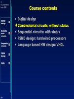
Course contents
•
Digital design
•
Combinatorial circuits: without status
Sequential circuits: with status
•
FSMD design: hardwired processors
•
Language based HW design: VHDL
3/2
©
R.Lauwereins
Imec 2001
Digital
design
Combina-
torial
circuits
Sequential
circuits
FSMD
design
VHDL
Sequential Circuits
•
The flip-flop as building block
•
Design of synchronous sequential
circuits
•
Design of asynchronous sequential
circuits
•
Basic RTL building blocks
3/3
©
R.Lauwereins
Imec 2001
Digital
design
Combina-
torial
circuits
Sequential
circuits
FSMD
design
VHDL
Sequential Circuits
The flip-flop as building block
•
Design of synchronous sequential
circuits
•
Design of asynchronous sequential
circuits
•
Basic RTL building blocks
3/4
©
R.Lauwereins
Imec 2001
Digital
design
Combina-
torial
circuits
Sequential
circuits
FSMD
design
VHDL
The flip-flop as building block
•
Definitions:
Combinatorial circuit: the output is function of
the current value of the inputs
Sequential circuit: the output is function of the
current value of the inputs and of the current
state (i.e. also function of the sequence of past
inputs)
3/5
©
R.Lauwereins
Imec 2001
Digital
design
Combina-
torial
circuits
Sequential
circuits
FSMD
design
VHDL
The flip-flop as building block
•
Definitions
Asynchronous sequential circuits: outputs and
state change as soon as an input changes
Synchronous sequential circuits: outputs and
state change only when a special input, the
clock, gets a certain value
Clock period: duration between two
consecutive 1→0 transitions of the clock
Clock frequency: 1 / (clock period)
Duty cycle: (duration that the clock equals 1) /
(clock period)
Rising edge: 0→1 transition of the clock
Falling edge: 1→0 transition of the clock
3/6
©
R.Lauwereins
Imec 2001
Digital
design
Combina-
torial
circuits
Sequential
circuits
FSMD
design
VHDL
Sequential Circuits
•
The flip-flop as building block
SR Latch
Gated SR Latch
Gated D Latch
Flip-flop sensitivity
Flip-flop types
•
Design of synchronous sequential
circuits
•
Design of asynchronous sequential
circuits
•
Basic RTL building blocks
3/7
©
R.Lauwereins
Imec 2001
Digital
design
Combina-
torial
circuits
Sequential
circuits
FSMD
design
VHDL
Sequential Circuits
•
The flip-flop as building block
SR Latch
Gated SR Latch
Gated D Latch
Flip-flop sensitivity
Flip-flop types
•
Design of synchronous sequential
circuits
•
Design of asynchronous sequential
circuits
•
Basic RTL building blocks
3/8
©
R.Lauwereins
Imec 2001
Digital
design
Combina-
torial
circuits
Sequential
circuits
FSMD
design
VHDL
SR Latch
Set
Reset
Q’
Q
S
R
Q
Q’
Undefined
S R Q(next)
0 0 Q
0 1 0
1 0 1
1 1 NA
3/9
©
R.Lauwereins
Imec 2001
Digital
design
Combina-
torial
circuits
Sequential
circuits
FSMD
design
VHDL
SR Latch
•
Note that a Boolean signal now already
consists of 5 values:
0: the logical signal “0”
1: the logical signal “1”
x: don’t care
Z: high impedant
U: undefined
•
The oscillation is called critical race
•
The oscillation only happens when the
delay of both gates is exactly equal
•
When the delays are not equal, the fastest
gates determines the end result:
implementation and run-time dependent ⇒
undefined
3/10
©
R.Lauwereins
Imec 2001
Digital
design
Combina-
torial
circuits
Sequential
circuits
FSMD
design
VHDL
SR Latch
Set
Reset
Q
Q’
S R Q(next)
1 1 Q
1 0 0
0 1 1
0 0 NA
Set and Reset active low
S
R
Q
Q’
3/11
©
R.Lauwereins
Imec 2001
Digital
design
Combina-
torial
circuits
Sequential
circuits
FSMD
design
VHDL
Sequential Circuits
•
The flip-flop as building block
SR Latch
Gated SR Latch
Gated D Latch
Flip-flop sensitivity
Flip-flop types
•
Design of synchronous sequential
circuits
•
Design of asynchronous sequential
circuits
•
Basic RTL building blocks
3/12
©
R.Lauwereins
Imec 2001
Digital
design
Combina-
torial
circuits
Sequential
circuits
FSMD
design
VHDL
Gated SR Latch
C S R Q(next)
0 0 0 Q
0 0 1 Q
0 1 0 Q
0 1 1 Q
1 0 0 Q
1 0 1 0
1 1 0 1
1 1 1 NA
C=1: follow inputs
C=0: latch outputs
Set
Reset
Q’
Q
Clock
3/13
©
R.Lauwereins
Imec 2001
Digital
design
Combina-
torial
circuits
Sequential
circuits
FSMD
design
VHDL
Sequential Circuits
•
The flip-flop as building block
SR Latch
Gated SR Latch
Gated D Latch
Flip-flop sensitivity
Flip-flop types
•
Design of synchronous sequential
circuits
•
Design of asynchronous sequential
circuits
•
Basic RTL building blocks
3/14
©
R.Lauwereins
Imec 2001
Digital
design
Combina-
torial
circuits
Sequential
circuits
FSMD
design
VHDL
Gated D Latch
C D Q(next)
0 0 Q
0 1 Q
1 0 0
1 1 1
C=1: follow input
C=0: latch output
D
Q’
Q
Clock
D→Q delay when C high: L-to-H delay: 2.4+1.4+1.4=5.2
H-to-L delay: 1+2.4+1.4=4.8
C→Q delay when D high: L-to-H delay: 2.4+1.4+1.4=5.2
when D low: H-to-L delay: 2.4+1.4=3.8
3/15
©
R.Lauwereins
Imec 2001
Digital
design
Combina-
torial
circuits
Sequential
circuits
FSMD
design
VHDL
Gated D Latch
C D Q(next)
0 0 Q
0 1 Q
1 0 0
1 1 1
C=1: follow input
C=0: latch output
D
Q’
Q
Clock
D must not change “immediately before” H-to-L of the
clock (during the setup time); reason: clock changes
between the switching of D and of D’ hence Set and
Reset switch from H to L at the same time ⇒ undefined
(setup time = H-to-L of invertor)
S
R
D
C
S
D’
R
3/16
©
R.Lauwereins
Imec 2001
Digital
design
Combina-
torial
circuits
Sequential
circuits
FSMD
design
VHDL
Gated D Latch
C D Q(next)
0 0 Q
0 1 Q
1 0 0
1 1 1
C=1: follow input
C=0: latch output
D
Q’
Q
Clock
When D switches at least setup time before the clock
transition, S and R will not switch from H to L at the
same time ⇒ OK (S is longer high than R, hence Q will
come high following the D input)
S
R
D
C
S
D’
R
3/17
©
R.Lauwereins
Imec 2001
Digital
design
Combina-
torial
circuits
Sequential
circuits
FSMD
design
VHDL
Gated D Latch
C D Q(next)
0 0 Q
0 1 Q
1 0 0
1 1 1
C=1: follow input
C=0: latch output
D
Q’
Q
Clock
Analogously, D may not switch “immediately after” H-to-L
of the clock (during the hold time)
S
R
5.2/3.8
D
C
Q
Q’
Symbol
Given values:
5.2=C to Q
L→H
3.8=C to Q
H→L
3/18
©
R.Lauwereins
Imec 2001
Digital
design
Combina-
torial
circuits
Sequential
circuits
FSMD
design
VHDL
Sequential Circuits
•
The flip-flop as building block
SR Latch
Gated SR Latch
Gated D Latch
Flip-flop sensitivity
Level-sensitive latch
Master-slave flip-flop
Edge-triggered flip-flop
Flip-flop types
•
Design of synchronous sequential
circuits
•
Design of asynchronous sequential
circuits
•
Basic RTL building blocks
3/19
©
R.Lauwereins
Imec 2001
Digital
design
Combina-
torial
circuits
Sequential
circuits
FSMD
design
VHDL
Sequential Circuits
•
The flip-flop as building block
SR Latch
Gated SR Latch
Gated D Latch
Flip-flop sensitivity
Level-sensitive latch
Master-slave flip-flop
Edge-triggered flip-flop
Flip-flop types
•
Design of synchronous sequential
circuits
•
Design of asynchronous sequential
circuits
•
Basic RTL building blocks
3/20
©
R.Lauwereins
Imec 2001
Digital
design
Combina-
torial
circuits
Sequential
circuits
FSMD
design
VHDL
Level sensitive latch
•
All previous gated latches are level
sensitive
Transparent when clock is high
Remembering the last value when clock is low
•
Level sensitive latches give problems for
shift registers for example
The input signal may ripple through multiple
stages during one clock-high phase
making it very hard to meet setup/hold time
requirements
See next slide
3/21
©
R.Lauwereins
Imec 2001
Digital
design
Combina-
torial
circuits
Sequential
circuits
FSMD
design
VHDL
Level sensitive latch
X
Clk
4/3
D
C
Q
1
4/3
D
C
Q
2
4/3
D
C
Q
3
Y
Two solutions:
•
Master-slave
•
Edge-triggered
Clk
X
Q
1
Q
2
Q
3
3/22
©
R.Lauwereins
Imec 2001
Digital
design
Combina-
torial
circuits
Sequential
circuits
FSMD
design
VHDL
Sequential Circuits
•
The flip-flop as building block
SR Latch
Gated SR Latch
Gated D Latch
Flip-flop sensitivity
Level-sensitive latch
Master-slave flip-flop
Edge-triggered flip-flop
Flip-flop types
•
Design of synchronous sequential
circuits
•
Design of asynchronous sequential
circuits
•
Basic RTL building blocks
3/23
©
R.Lauwereins
Imec 2001
Digital
design
Combina-
torial
circuits
Sequential
circuits
FSMD
design
VHDL
Master-slave flip-flop
4/3
D
C
Q
s1
4/3
D
C
Q
m1
Master Slave
4/3
D
C
Q
s2
4/3
D
C
Q
m2
Master Slave
X
Q
1
Clk
Y
Clk
X
Q
m1
Q
1
Q
m2
Y
The master clocks at the falling clock edge
The slave clocks at the rising edge
3/24
©
R.Lauwereins
Imec 2001
Digital
design
Combina-
torial
circuits
Sequential
circuits
FSMD
design
VHDL
Sequential Circuits
•
The flip-flop as building block
SR Latch
Gated SR Latch
Gated D Latch
Flip-flop sensitivity
Level-sensitive latch
Master-slave flip-flop
Edge-triggered flip-flop
Flip-flop types
•
Design of synchronous sequential
circuits
•
Design of asynchronous sequential
circuits
•
Basic RTL building blocks
3/25
©
R.Lauwereins
Imec 2001
Digital
design
Combina-
torial
circuits
Sequential
circuits
FSMD
design
VHDL
Edge-triggered flip-flop
Set Latch
Reset Latch
Output
Latch
Clk
D
Reset
A
Set
B
Q
Q’
Clk
D
B
A
R
S
Q