- Trang chủ >>
- Khoa Học Tự Nhiên >>
- Vật lý
ordered porous nanostructures and applications, 2005, p.211
Bạn đang xem bản rút gọn của tài liệu. Xem và tải ngay bản đầy đủ của tài liệu tại đây (11.94 MB, 211 trang )
Ordered Porous Nanostructures
and Applications
Edited by
Ralf B. Wehrspohn
Department of Physics
University of Paderborn
Paderborn, Germany
Nanostructure Science and Technology
Series Editor: David J. Lockwood, FRSC
National Research Council of Canada
Ottawa, Ontario, Canada
Current volumes in this series:
Ordered Porous Nanostructures and Applications
Edited by Ralf B. Wehrspohn
Surface Effects in Magnetic Nanoparticles
Dino Fiorani
Alternative Lithography: Unleashing the Potentials of Nanotechnology
Edited by Clivia M. Sotomayor Torres
Interfacial Nanochemistry: Molecular Science and Engineering at Liquid-Liquid Interfaces
Edited by Hitoshi Watarai
Introduction to Nanoscale Science and Technology, Vol. 6
Di Ventra, Massimiliano; Evoy, Stephane; Helflin Jr., James R.
Nanoparticles: Building Blocks for Nanotechnology
Edited by Vincent Rotello
Nanostructured Catalysts
Edited by Susannah L. Scott, Cathleen M. Crudden, and Christopher W. Jones
Nanotechnology in Catalysts, Volume 1 and 2
Edited by Bing Zhou, Sophie Hermans, and Gabor A. Somorjai
Polyoxometalate Chemistry for Nano-Composite Design
Edited by Toshiro Yamase and Michael T. Pope
Self-Assembled Nanostructures
Jin Z. Zhang, Zhong-lin Wang, Jun Liu, Shaowei Chen, and Gang-yu Liu
Semiconductor Nanocrystals: From Basic Principles to Applications
Edited by Alexander L. Efros, David J. Lockwood, and Leonid Tsybeskov
A Continuation Order Plan is available for this series. A continuation order will bring delivery of each new volume immediately
upon publication. Volumes are billed only upon actual shipment. For further information please contact the publisher.
Ordered Porous Nanostructures
and Applications
Ralf B. Wehrspohn
Department of Physics
University of Paderborn
Paderborn, Germany
Library of Congress Cataloging-in-Publication Data
Wehrspohn, Ralf B.
Ordered porous nanostructures and applications / Ed. by Ralf B. Wehrspohn.
p. cm.—(Nanostructure science and technology)
Includes bibliographical references and index.
ISBN 0-387-23541-8
1. Nanotechnology. 2. Nanostructures. I. Title. II. Series.
T174.7.W44 2005
620
.5—dc22 2004062627
ISBN 0-387-23541-8
C
2005 Springer Science+Business Media, Inc.
All rights reserved. This work may not be translated or copied in whole or in part without
the written permission of the publisher (Springer Science+Business Media, Inc., 233 Spring
Street, New York, NY 10013, USA), except for brief excerpts in connection with reviews or
scholarly analysis. Use in connection with any form of information storage and retrieval,
electronic adaptation, computer software, or by similar or dissimilar methodology now
known or hereafter developed is forbidden.
The use in this publication of trade names, trademarks, service marks and similar terms,
even if they are not identified as such, is not to be taken as an expression of opinion as to
whether or not they are subject to proprietary rights.
Printed in the United States of America.
987654321
springeronline.com
Contributors
J. Carstensen
Material Science Department,
Faculty of Engineering
Christian-Albrechts University,
Kaiserstraße 2, D-24143, Kiel,
Germany
J N. Chazalviel
Laboratoire de Physique
de la Mati`ere Condens´ee,
CNRS-Ecole Polytechnique,
91128 Palaiseau Cedex,
France
M. Christophersen
Material Science Department,
Faculty of Engineering
Christian-Albrechts University,
Kaiserstraße 2, D-24143, Kiel,
Germany
H. F¨oll
Material Science Department,
Faculty of Engineering
Christian-Albrechts University,
Kaiserstraße 2, D-24143, Kiel,
Germany
P.J. French
Electronic Instrumentation Laboratory,
Department of Microelectronics,
Faculty of Electrical Engineering,
Mathematics and Computer Science,
Delf University of Technology,
Mekelweg 4, 2628 CD Delf,
The Netherlands
L.V. Govor
Institute of Physics,
University of Oldenburg,
D-26111 Oldenburg,
Germany
Siegmund Greulich-Weber
Physics Department,
Faculty of Science,
University of Paderborn,
D-33095 Paderborn,
Germany
Riccardo Hertel
Dept. of Solid State
Research, Research Center Juelich,
D-52425 Juelich,
Germany
S. Langa
Material Science Department,
Faculty of Engineering
Christian-Albrechts University,
Kaiserstraße 2, D-24143, Kiel,
Germany
and
Laboratory of Low Dimensional
Semiconductor Structures,
v
vi CONTRIBUTORS
Technical University of Moldova,
St. cel Mare 168, MD-2004, Chisinau,
Moldova
V. Lehmann
Infineon Technologies AG,
Dept. CPS EB BS,
Otto-Hahn-Ring 6,
D-81730 M¨unchen,
Germany
Heinrich Marsmann
Faculty of Science,
University of Paderborn,
D-33095 Paderborn,
Germany
Hideki Masuda
Department of Applied Chemistry,
Tokyo Metropolitan University,
1-1 Minamiosawa, Hachioji,
Tokyo 192-03,
Japan
Kornelius Nielsch
Max-Planck-Institute of
Microstructure Physics,
Weinberg 2D-06120 Halle,
Germany
H. Ohji
Mitsubishi Electric Corporation,
Advanced Technology Research
and Development Centre,
Amagasaki, Hyogo 6618661,
Japan
F. Ozanam
Laboratoire de Physique
de la Mati`ere Condens´ee,
CNRS-Ecole Polytechnique,
91128 Palaiseau Cedex,
France
Joerg Schilling
California Institute of Technology,
Pasadena, CA 91125,
USA
I.M. Tiginyanu
Laboratory of Low Dimensional
Semiconductor Structures,
Technical University of Moldova,
St. cel Mare 168, MD-2004, Chisinau,
Moldova
Ralf B. Wehrspohn
Department of Physics,
University of Paderborn,
D-33095 Paderborn,
Germany
Foreword
Numerous major advances in research and technology over the last decade or two have
been made possible by the successful development of nanostructures made of metals, in-
sulators and especially semiconductors. Nanostructures are man-made objects that have
one, two or three dimensions in the sub-micrometre to nanometre regime. Nanostruc-
tures made of semiconductor quantum wells, which consist of alternating layers of two
different semiconductors with typical thicknesses in the sub-10 nm regime, were first
demonstrated more than 20 years ago. Today, they are at the heart of most semicon-
ductor lasers. More recently, carbon nanotubes and semiconductor quantum dots have
attracted a lot of scientific attention because of their unique properties and their wide-
ranging potential applications. Even the dominant industry since the late-20th century
have embraced the use of nanostructures. Indeed, in the microelectronic industry, the
size of individual transistors is well below 100 nm and within 10 years may approach
the regime where quantum size effects start playing a role.
One significant difficulty with nanostructures is how to prepare them. One can
distinguish two approaches: top-down and bottom-up. In the top-down approach, objects
of ever-smaller dimensions are carved out of larger objects. This approach is taken in
the semiconductor industry where advanced lithography aided by specific steps such
as selective oxidation has unrelentlessly shrunk the typical dimensions to well below
1 μm. However, this approach is increasingly complicated and expensive. The bottom-
up approach consists of growing small objects to their desired size and shape. This is
usually accomplished by chemical means. This approach is very flexible and usually
inexpensive, but it too suffers from significant problems, chief among them are size and
positioning control and throughput.
Porous nanostructures have attracted a lot of attention because they combine many
of the advantages of the top-down and bottom-up approaches. The typical dimension can
be varied from a few nanometres to many micrometres, the porous structures be made
in many materials and be ordered, and entire wafers can be processed in minutes. Since
1990, a lot of effort has been devoted to understanding and controlling the pore formation
mechanism and to evaluating the usefulness of porous nanostructures in technology. This
book, edited by Ralf Wehrspohn, is a very timely and excellent review of the state of
the art in ordered porous nanostructures and their applications. It contains nine chapters
written by leading experts. The chapters on materials and preparations cover the most
vii
viii FOREWORD
important porous materials, namely silicon, III–V semiconductors, alumina and poly-
mers. These chapters cover all the important aspects of the fascinating materials science
of porous materials. Topics ranging from well-understood phenomena to still controver-
sial observations are discussed. The second part of the book is devoted to applications.
The last three chapters cover the important applications in optics, magnetics and micro-
machining.
This book will be valuable to all researchers active in the field, whether they are
experienced or just starting, and whether they are in research or development.
Philippe M. Fauchet
Rochester, NY
Preface
In the 1990s, a variety of two-dimensional self-ordered porous nanostructures were dis-
covered. Starting with ordered macroporous silicon discovered by Lehmann and F¨oll
in 1990, other self-ordered materials were discovered: self-ordered porous alumina by
Masuda and Fukuda in 1995, self-ordered diblock copolymers aligned on substrates by
the Russel group in 1994, self-ordered zeolites (MCM-41) by the Mobil Oil group in
1992, self-ordered porous polymer structures with honeycomb morphology by Francois
and co-workers in 1994 and finally self-ordered porous group III–V semiconductors by
F¨oll and co-workers in 1999. Similarly, also three-dimensional self-ordered nanostruc-
tures developed in the same decade like three-dimensionally arranged block copolymers
and 3D colloidal self-assembly.
This edited book presents the synthesis of the five materials systems mentioned
above and tries to explain the physical and chemical mechanisms of self-ordering. In
general, ordering is always due to repulsive or attractive forces between the pores leading
in two dimensions to the hexagonal lattice. In three dimensions, stacking can either lead to
the fcc or hcp lattice, but it is always a closed-packed configuration. These ordered porous
nanostructures are very attractive for template synthesis of nanowires or nanotubes or
in 3D even of more complex structures, and a number of examples of ordered porous
nanostructures are given in different chapters.
The last three chapters describe three very prominent areas of applications of
these materials: photonics, magnetic storage media and nano-electromechanical systems
(NEMS).
Ralf Wehrspohn
Paderborn, Germany
ix
Contents
I. MATERIALS AND PREPARATIONS
CHAPTER 1. Electrochemical Pore Array Fabrication on n-Type
Silicon Electrodes 3
V. Lehmann
1.1 Why the first artificial pore arrays were realized in n-type
silicon electrodes 3
1.2 The physics of pore initiation on silicon electrodes in HF 4
1.3 The photolithographic pre-structuring process and the anodization
set-up 8
1.4 Limiting factors and design rules for macropore arrays on n-type
silicon electrodes 9
CHAPTER 2. Macropores in p-Type Silicon 15
J N. Chazalviel and F. Ozanam
2.1 Introduction 15
2.2 Phenomenology 16
2.3 Theory 22
2.4 Discussion 28
2.5 Ordered macropore arrays 32
2.6 Conclusion 33
CHAPTER 3. Highly Ordered Nanohole Arrays in Anodic Porous Alumina 37
Hideki Masuda
3.1 Introduction 37
3.2 Naturally occurring long-range ordering of the hole configuration
of anodic alumina 38
3.3 Two-step anodization for ordered arrays with straight holes
in naturally ordering processes 40
3.4 Ideally ordered hole array using pretexturing of aluminum 41
3.5 Self-repair of the hole configuration in anodic porous alumina 45
xi
xii CONTENTS
3.6 Modification of the shape of hole opening in the anodic
porous alumina 46
3.7 Nanofabrication based on highly ordered anodic alumina 48
3.8 Conclusion 53
CHAPTER 4. The Way to Uniformity in Porous III–V Compounds Via
Self-Organization and Lithography Patterning 57
S. Langa, J. Carstensen, M. Christophersen, H. F
¨
oll
and I.M. Tiginyanu
4.1 Introduction 57
4.2 Aspects of Chemistry and Electrochemistry of Semiconductors 60
4.3 Pore morphologies observed in III–V compounds 65
4.4 Self-organized processes during pore formation in III–V compounds 73
4.5 Possible applications of III–V porous structures 80
4.6 Conclusion 84
CHAPTER 5. Microporous Honeycomb-Structured Polymer Films 89
L.V. Govor
5.1 Introduction 89
5.2 Experimental formation of polymer honeycomb structures 90
5.3 Self-assembled networks of polymers 92
5.4 Model for the formation of the honeycomb structures in
polymer films 95
5.5 Application of polymer networks 103
5.6 Conclusion 105
CHAPTER 6. From Nanosize Silica Spheres to Three-Dimensional
Colloidal Crystals 109
Siegmund Greulich-Weber and Heinrich Marsmann
6.1 Introduction 109
6.2 Synthesis of colloidal silica nanospheres 110
6.3 Growth of colloidal crystals 119
6.4 Three-dimensional periodic nanoporous materials 128
6.5 Applications 130
6.6 Concluding remarks 132
II. APPLICATIONS
CHAPTER 7. Macroporous Silicon Photonic Crystals 145
Ralf B. Wehrspohn, Joerg Schilling
7.1 Introduction 145
7.2 2D photonic crystals on the basis of macroporous silicon 146
7.3 Defects in 2D macroporous silicon photonic crystals 152
CONTENTS xiii
7.4 2D photonic crystals in the NIR 156
7.5 Tunability of Photonic band gaps 158
7.6 3D photonic crystals on the basis of macroporous silicon 159
7.7 Summary 161
CHAPTER 8. High-Density Nickel Nanowire Arrays 165
Kornelius Nielsch, Riccardo Hertel and Ralf B. Wehrspohn
8.1 Introduction 165
8.2 Experimental details 166
8.3 Magnetic properties of nickel nanowire arrays 169
8.4 Nickel nanowire arrays with 2D single crystalline arrangement 173
8.5 Micromagnetic modelling 175
8.6 Conclusion 183
CHAPTER 9. Porous Silicon for Micromachining 185
P.J. French and H. Ohji
9.1 Introduction 185
9.2 Basic process 186
9.3 Applications 197
9.4 Conclusions 203
Index 205
I
MATERIALS AND
PREPARATIONS
1
Electrochemical Pore Array
Fabrication on n-Type
Silicon Electrodes
V. Lehmann
Infineon Technologies AG, Dept. CPS EB BS, Otto-Hahn-Ring 6, D-81730 M
¨
unchen, Germany
volker.lehmann@infineon.com
1.1. WHY THE FIRST ARTIFICIAL PORE ARRAYS WERE REALIZED
IN N-TYPE SILICON ELECTRODES
The surface morphology of a solid-state electrode after an electrochemical dissolution
process depends sensitively on the parameters of anodization. The one extreme case is
an anodization condition under which even a rough electrode surface becomes homoge-
neously smooth, this process has been termed electropolishing. If in contrast the surface
becomes rougher, we deal with corrosion or pore formation. In the prior case, commonly
the crevice geometry is random and no narrow size regime is observed. This is different
in the latter case. Electrochemically formed porous materials usually show a narrow
pore size distribution and a certain pore density, which allows us to determine the ratio
of pore volume to the total volume, the porosity. In most cases, the pore distribution at
the electrode surface is random; however, in certain cases, like for example, for porous
alumina, a short-range order may be observed. Pore arrays with a long-range order of the
pore positions, which are desirable for a multitude of applications, can only be produced
artificially.
The fact that n-type silicon was the first electrode material on which pore arrays of
such a long-range order have been realized is not purely accidental. For artificial pat-
terning, the electrochemical pore initiation process must be understood and a structuring
technique must be available. In many electrode–electrolyte systems, the pore initiation
mechanism is complex and still under debate, as for example, for pore formation in
aluminium [1]. In other systems, like alumina, the pore size is small and just becomes
3
4 CHAPTER 1
assessable for today’s most advanced structuring technologies [2]. In contrast, in low-
doped n-type silicon electrodes, to a large extent, the pore initiation is simply controlled
by the interface topography and the pore size is well measured in the micrometre regime.
This enabled us about a decade ago to use the standard silicon process technology avail-
able at that time, such as thin film deposition, photolithography, and wet etching, to
generate a pore initiation pattern. Upon anodization in hydrofluoric acid (HF) this arbi-
trary pattern developed into an array of straight pores [3]. The resulting pore morphology
can be inspected by cleaving the silicon electrode and subsequent optical microscopy
(OM) or scanning electron microscopy (SEM).
Over the years, the electrochemical etching process has been optimized and today
the pore array may cover a whole silicon wafer and penetrate its full thickness. Further-
more, pore arrays have been realized by the anodization of a multitude of other materials
as discussed in subsequent chapters.
1.2. THE PHYSICS OF PORE INITIATION ON SILICON ELECTRODES IN HF
In order to predetermine the position of an electrochemically formed pore a de-
tailed understanding of the pore initiation process is required. The pore initiation may,
for example, be dominated by the impurity or defect distribution, by the state of electrode
passivation, or by the topography of the electrode surface. As a consequence, structuring
techniques for electrochemical pore array fabrication could be based on local impu-
rity implantation, depassivation, or etching of depressions to generate pore initiation
sites.
For the case of n-type silicon an anodic oxide has been discussed as a potential
candidate for passive film formation. An indispensable constituent of all electrolytes
for pore formation in silicon electrodes, however, is hydrofluoric acid, which readily
dissolves SiO
2
. Pore initiation by defects is unlikely as well, because today’s silicon
crystals are manufactured free of defects and with atomic impurity levels down to 10
12
cm
−3
. The third of the above options, the topography of the electrode surface, has been
found to be the relevant factor for the pore initiation process.
All pore formation on silicon electrodes is observed in an anodic regime where the
dissolution reaction is limited by charge supply from the electrode. This regime is charac-
terized by an anodic current density below a critical value J
PS
. J
PS
depends on electrolyte
concentration, temperature and crystal orientation of the electrode [4]. The dissolution
reaction is initiated by a hole (defect electron), reaching the silicon–electrolyte interface.
Since charge supply is the limiting factor dissolution occurs preferentially at sites which
attract holes. If no such sites are present, like for example, for an atomically flat elec-
trode the dissolution starts homogeneously. However, any inhomogeneity of dissolution
will be amplified and within seconds etch pits are formed, which act as initiation sites
for pore growth. This random pore initiation process at polished electrode surfaces is
shown in Figure 1.1. Note that in the first 30 seconds of anodization a very high density
of nanometre-sized etch pits are generated. In the next 30 seconds, a few of these pits
increase their size by a factor of 5 or more consuming neighbouring pits. This process
continues until the number of surviving pores becomes constant. This is the case, after
about 240 seconds, for an n-type doping concentration of 10
16
cm
−3
.
PORES IN N-TYPE SILICON 5
FIGURE 1.1. SEM micrographs of spontaneous pore initiation on polished surfaces of n-type Si electrodes
anodized for the indicated times under white light illumination of the front side (14 V, 2.5% HF, 10 mA/cm
−2
,
n-type Si 10
16
cm
−3
(100)). Microporous silicon covering the macropores, as shown on the top row (cross-
sectional view), has been removed by alkaline etching for better visibility at centre (cross-sectional view)
and the bottom row (surface view). From Ref. [1].
If depressions are already present in the electrode prior to anodization, it is easily
understood that they become initiation sites for the pore formation. A pattern of artificial
initiation sites works only as desired, if its pitch is close to the pore spacing that develops
spontaneously on the silicon electrode upon anodization. The average distance of random
pores is usually in the same order of magnitude as the pore diameter. The observed
diameters of pores formed in silicon electrodes cover four orders of magnitude and is
classified in three size regimes. A porous film is designated microporous if the pore
diameter is below 2 nm. In this size regime, pore formation is dominated by quantum
size effects. While the pore size becomes mesoporous (2 nm < pore diameter < 50 nm)
or macroporous (pore diameter > 50 nm) if the formation process is dominated by the
electric field in the space–charge region (SCR). In the electric field dominated case, the
morphology of the porous structure depends sensitively on the way the charge carriers
pass through the SCR. An overview of the different size regimes and the proposed pore
formation mechanism is displayed in Figure 1.2. The fact that the pore initiation site
can be predetermined by a depression in the electrode surface has first been shown for
macropores in low-doped n-type electrodes for which the pore formation is dominated by
minority carrier collection. Later on, however, it has been shown that for the other three
field-dominated pore formation effects, as displayed in Figure 1.2, a depression is as
well sufficient as initiation site [5]. Figures 1.3b–d show arrays of macropores on p-type
silicon, the pores initiate preferentially at the pyramidal depression in the pre-structured
electrode surface. Figure 1.3e shows a minute mesopore formed by tunnelling of charge
6 CHAPTER 1
FIGURE 1.2. Effects proposed to be responsible for pore wall passivation (top row). Effects which can lead to
passivation breakdown at the pore tip (middle row) and the resulting kind of porous silicon structure together
with substrate doping type (bottom row). From Ref. [5].
FIGURE 1.3. Electrochemical pore formation in silicon electrodes of different kinds and density of dop-
ing initiated by an artificial depression. (a–d) Pore initiation on a polished (a) and on patterned (b–d) p-
type silicon electrodes (2 mA/cm
2
, 3% HF, 240 minutes, p-type Si 3 × 10
14
cm
−3
) (OM after [6]). (e)
Mesopore formation at the tip of a pyramidal etch pit (10 V, 6% HF, 5 seconds, n-type Si 10
15
cm
−3
)
(SEM after [4]). (f) A large circular etch pit structure formed by avalanche breakdown (50 V, 6% HF, 100
seconds, n-type Si 10
15
cm
−3
). Note that the structure is centred around the pyramidal initiation etch pit
(SEM from Ref. [5]).
PORES IN N-TYPE SILICON 7
FIGURE 1.4. SEM micrographs of surface, cross section and a 45
◦
level of anodized n-type silicon samples
(10
15
cm
−3
). Sample (a) shows randomly distributed pores due to anodization of a polished electrode, while
sample (b) shows a square array of pores generated by anodization of a patterned surface. The pore initiation
pattern, as shown in the inset, has been produced by photolithography and alkaline etching. From Ref. [4].
carriers located at the tip of a depression. Figure 1.3f shows that a large cavity formed
by avalanche breakdown is also centred at the tip of an artificial depression. It can be
speculated that even the initiation of micropores is sensitive to the electrode topology. In
order to test this hypothesis, however, the required resolution of the initiation pattern has
to be in the order of 1 nm and is therefore beyond today’s photolithographic structuring
techniques.
The density of random pores in n-type silicon electrodes decreases with decreasing
substrate-doping density. For an n-type doping concentration of 10
15
cm
−3
, as shown in
Figure 1.4a, the pore initiation process takes longer and the final pore density is lower, as
for example shown for an n-type doping concentration of 10
16
cm
−3
in Figure 1.1. This
dependence of pore density on the doping level of the bulk silicon reflects the influence
of the SCR width on the formation process of initiation sites. A depression produces a
deformation of the SCR and the electric field becomes maximum where the radius of
curvature of the depression has its minimum. For the case of highly doped silicon the
electric field easily reaches its breakdown value even for moderate applied bias if the
tip radius is reduced to a few tens of nanometres. As a consequence, the tunnelling of
charge carriers is confined to the tip of the depression. In low-doped silicon, where the
field strength is usually below the breakdown value, the transfer of charge carriers is still
influenced by the topography and shows a maximum at the tip of the depression. Even if
the field of the SCR is neglected and pure hole diffusion is considered, a depression is
still a favourable location for charge transfer. In the case of low-doped n-type silicon
electrodes the electric field as well as the diffusion have to be considered for pore initiation
and pore growth [5,6].
8 CHAPTER 1
In conclusion, a flat silicon electrode anodized in HF below the critical current
density is unstable. Such a system shows a tendency to enhance inhomogeneities of the
surface topography. An artificial pore initiation pattern realized by depression in the
electrodes surface exploits this instability to form pore arrays. An example of such a
pore array is shown in Figure 1.4b. The array of etch pits used for initiation is shown in
the inset of this figure.
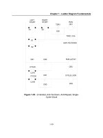
1.3. THE PHOTOLITHOGRAPHIC PRE-STRUCTURING PROCESS
AND THE ANODIZATION SET-UP
A depression, sufficient for pore initiation in an n-type electrode, can be realized
in many ways. Most compatible with today’s semiconductor manufacturing techniques
is photolithographic structuring. The basic process sequence is sketched in Figure 1.5.
A thermal oxide is formed on a polished, (100)-oriented, n-type silicon wafer with a
highly doped n-type backside layer. A photoresist is then deposited on the front side and
illuminated using a mask with the desired pore pattern. Subsequently windows in the
oxide film are opened, using a plasma etch process, for example. A wet alkaline etching
FIGURE 1.5. Schematic view of the fabrication process of pore arrays in n-type silicon electrodes.
PORES IN N-TYPE SILICON 9
process then generates sharp-tipped etch pits that show the geometry of an inverted
pyramid, as shown in the inset of Figure 1.4b. These etch pits act as initiation sites for
the electrochemical etching process, because their collection efficiency for holes (defect
electrons), generated by illumination of the electrode backside, is much better than the
one for the flat substrate.
The pore initiation process is sensitive to the geometry of the depression. For a
depression with a large radius of curvature at the bottom, for example, the starting
position of the pore is badly defined. As a consequence, a certain mispositioning of
the pores in an array can be expected. An inverted pyramid with a flat bottom, for
example, can be realized by a reduction of alkaline etching time. For such a geometry,
the formation of four pores located at the four corners of the inverted pyramid bottom
has been observed.
The electrolyte used for macropore array formation in n-type Si electrodes is com-
posed of aqueous HF. The pore growth rate depends sensitively on HF concentration
(commonly 1–10%) and is in the order of 1 μm/min. Hydrogen is a by-product of the
electrochemical dissolution process. In order to reduce the sticking probability of hy-
drogen bubbles to the electrode surface, addition of a detergent and strong electrolyte
agitation are recommended. PVC or PP is recommended as materials for the cell body.
Standard O rings (nitrile polymer) are found to be stable in the HF electrolyte. A platinum
electrode is commonly used as cathode. A reference electrode is not required because the
pore formation process on n-type silicon is not very sensitive to bias. The highly doped
backside electrode is connected to the positive side of the power supply, collecting the
photo-generated electrons.
The light source used for illumination of the n-type electrode should emit at wave-
lengths below 900 nm, because longer wavelengths penetrate deep into the bulk and
might generate charge carriers in the pore walls. Such light sources can be realized by
LEDs or by a filament lamp with an optical short-pass filter.
1.4. LIMITING FACTORS AND DESIGN RULES FOR MACROPORE ARRAYS
ON N-TYPE SILICON ELECTRODES
Not all desirable macropore array geometries can be realized by the electrochemical
etching process. This section gives the upper and lower limits for pore dimensions and
a few design rules [7].
The realization of a desired pore pattern requires a certain doping density of the
n-type Si electrode. A good rule of thumb for the selection of an appropriate substrate
is to multiply the desired pore density given (in μm
2
)by10
16
and take this number as
doping density (in cm
−3
). This dependency is shown in Figure 1.6. A square pattern of
10 μm pitch, for example, produces a pore density of 0.01 pores/μm
2
which can be best
etched using a substrate of an n-type doping density of 10
14
cm
−3
. A maladjustment of
pore pattern and substrate doping density will lead to branching of pores, as shown in
Figure 1.7a or dying of pores, as shown in Figure 1.7c.
The number of possible arrangements of the pore pattern is only limited by the re-
quirement that under homogeneous backside illumination the porosity has to be constant
on a length scale above about three times the pitch. This means it is possible to etch a
10 CHAPTER 1
FIGURE 1.6. Pore density versus silicon electrode doping density for porous silicon layers of different size
regimes. The dashed line shows the pore density of a triangular pore pattern with a pore pitch equal to two
times the SCR width for 3 V applied bias. Note that only macropores on n-type substrates may show a pore
spacing significantly exceeding this limit. The regime of stable macropore array formation on n-type Si is
indicated by a dot pattern. Type of doping and the formation of current density (in mA/cm
2
) are indicated in
the legend. From Ref. [5].
FIGURE 1.7. SEM micrographs of macropore array morphology for the same initiation pattern applied
to differently doped n-type electrodes (2.5% HF, 5 mA/cm
2
, 2 V). (a) For the highly doped electrode the
pitch of the pattern is too coarse, which leads to branching. (c) For the low-doped substrate the pattern
is too fine which results in dying of pores. (b) Doping density and pitch are well adjusted in this case and
branching is only observed at the border to an unpatterned area (underetching indicated by white dashed line).
From Ref. [7].
PORES IN N-TYPE SILICON 11
FIGURE 1.8. Sketches showing cross sections of macropore arrays orthogonal to the growth direction (a) for
a square, (b) for an ordered and (c) for a random pattern. The pores (black squares) collect holes from the area
indicated by the dashed lines. The porosity (the ratio of the black area to the total area) is 0.25 for all patterns.
pattern with a missing pore, a missing row of pores or even two missing rows. Patterns
as shown in Figure 1.8b can also be etched. A single pore, however, cannot be etched. It
is also possible to enlarge or shrink the pitch of a pattern across the sample surface by a
maximum factor of about 3. But a pattern with an abrupt border to an unpatterned area
will lead to severe underetching according to Figure 1.7b and random pore formation in
the unpatterned area.
A local variation of porosity can be produced by an inhomogeneous illumina-
tion intensity. However, any image projected on the backside of the wafer generates a
smoothed-out current density distribution on the front side, due to random diffusion of
the charge carriers in the bulk. This problem can be reduced if thin wafers or illumination
of the front side is used. However, sharp lateral changes of porosity cannot be realized.
Arrays with pore diameters d as small as about 0.3 μm have been realized [7]. The
lower limit for the pore diameter of an ordered array is established by breakdown, which
leads to light-independent pore growth and spiking. There seems to be no upper limit
for the pore diameter, because the formation of 100 μm wide pores has been shown to
be feasible [8]. Array porosities may range from 0.01 to close to 1. The porosity, which
is controlled by the etching current, determines the ratio between the pore diameter and
the pitch of the pore pattern. This means for a square pattern, any pore diameter between
one-tenth of the pitch and nearly the pitch can be realized.
The pore diameter can be varied over the length of the pore by a factor up to about
3 for all pores simultaneously by adjusting the current density, as visualized by Figure
1.9. This means the porosity normal to the surface can be varied. The taper of such pore
geometries is limited by dying of pores to values below about 30
◦
for a pore diameter
decreasing in growth direction, while values in the order of 45
◦
have been realized for an
increase of pore diameter in growth direction [9]. Note that narrow bottlenecks will sig-
nificantly reduce the diffusion in the pore and the formation of deep modulated pores be-
comes more difficult than the formation of straight pores. Bottlenecks at the pore entrance
may result from the transition of the pyramidal etch pit into a poretip. They can be avoided
by an increase of the current density during the first minutes of pore array fabrication.
The pore cross section under stable array formation conditions is usually a rounded
square, as shown in Figure 1.10b. Subsequent to electrochemical pore formation, the
cross section can be made round by oxidation steps or can be made square by chemical
12 CHAPTER 1
FIGURE 1.9. A sine wave modulation of the etching current versus etching time produces an array of
macropores with corresponding modulation of a diameter. From Ref. [7].
etching at RT in aqueous HF or weak alkaline solutions such as diluted KOH or NH
4
OH.
The formation of side pores by branching or spiking, as shown in Figure 1.7a, can be
suppressed by an increase of current density or a decrease of doping density, bias or HF
concentration. The dying of pores, as shown in Figure 1.7c, is suppressed by an increase
of current density, doping density or bias.
The pore length l can be as large as the wafer thickness (up to 1 mm). However,
the growth of deep pores requires low electrolyte concentrations, low temperatures and
etching times in the order of a day or more, because the etch rate in deep pores is limited
by HF diffusion to values in the order of 0.5 μm/min and below. Shorter pores (l < 0.1
mm) can be etched much faster (5 μm/min). Under stable etching conditions all pores
have the same length. Pore arrays with through-pores can be realized by an increase of the
etching current density into the electropolishing regime, which separates a free-standing
porous plate from the substrate. Macropores penetrating the whole wafer thickness can be
etched as well, however, pore formation becomes unstable in the vicinity of the backside.
The formation of dead-end pores and subsequent oxidation and alkaline etchback has
found to be technologically favourable.
FIGURE 1.10. By an increase of bias or doping density the round (a) or slightly faceted (b) cross section of
macropores becomes star shaped by branching (c and d) or spiking (e) along the 100 directions orthogonal
to the growth direction.
PORES IN N-TYPE SILICON 13
Another effect which limits the obtainable pore length is characterized by a sudden
drop of the growth rate at the pore tip to negligible values and an increase of pore diam-
eter close to the tip. This degradation of pore growth establishes an upper limit for the
pore length for a given set of anodization parameters. The fact that pore degradation is
delayed for a reduced formation current, which produces conical pores is an indication
for a diffusion related phenomenon. The observed dependence of degradation on the con-
centration of the dissolution product H
2
SiF
6
in the electrolyte points to a poisoning of
the dissolution reaction. The maximum obtainable pore depth decreases rapidly with in-
creasing HF concentration. This effect has been ascribed to the rate of H
2
SiF
6
production
being proportional to J
PS
which again depends exponentially on HF concentration, while
the diffusion of H
2
SiF
6
is expected to show little dependence on HF concentration [7].
The pore growth direction is along the 100 direction and toward the source of
holes. For the growth of perfect macropores perpendicular to the electrode surface (100)-
oriented Si substrates are required. Tilted pore arrays can be etched on substrates with a
certain misorientation to the (100) plane. Misorientation, however, enhances the tendency
of branching and angles of about 20
◦
seem to be an upper limit for unbranched pores.
In conclusion, it can be said that the limits of macropore array formation are in some
way complementary to the limitations of plasma etching. The latter technique gives a
higher degree of freedom in lateral design, while the freedom in vertical design and the
feasible pore aspect ratios is limited.
Today’s applications of macropore arrays range from electronic applications such
as capacitors to optical filters and biochips.
REFERENCES
[1] T. Martin and K.R. Hebert, Atomic force microscopy study of anodic etching of aluminum, J. Electrochem.
Soc. 148, B101–B109 (2001).
[2] H. Masuda and K. Fukuda, Science 268, 1466 (1995).
[3] V. Lehmann and H. F¨oll, Formation mechanism and properties of electrochemically etched trenches in
n-type silicon, J. Electrochem. Soc. 137, 653–659 (1990).
[4] V. Lehmann, R. Stengl and A. Luigart, On the morphology and the electrochemical formation mechanism
of mesoporous silicon, Mater. Sci. Eng. B 69–70, 11–22 (2000).
[5] V. Lehmann, The physics of macropore formation in low doped n-type silicon, J. Electrochem. Soc. 140,
2836–2843 (1993).
[6] V. Lehmann and S. R¨onnebeck, The physics of macropore formation in low doped p-type silicon, J.
Electrochem. Soc. 146, 2968–2975 (1999).
[7] V. Lehmann and U. Gr¨uning, The limits of macropore array fabrication, Thin Sol. Films 297, 13–17 (1997).
[8] P. Kleinmann, J. Linnros and S. Peterson, Formation of wide and deep pores in silicon by electrochemical
etching, Mater. Sci. Eng. B 69–70, 29–33 (2000).
[9] F. M¨uller, A. Birner, J. Schilling, U. G¨osele, C. Kettner and P. H¨anggi, Membranes for micropumps from
macroporous silicon, Phys. Status Solidi a 182, 585 (2000).
2
Macropores in p-Type Silicon
J N. Chazalviel and F. Ozanam
Laboratoire de Physique de la Mati
`
ere Condens
´
ee, CNRS-Ecole Polytechnique, Palaiseau, France
E-mail:
2.1. INTRODUCTION
Anodization of moderately doped (N
A
∼ 10
15
–10
16
cm
−3
) p-Si substrates in aqueous
or ethanolic HF has long been the most popular method for obtaining good quality
microporous silicon [1,2]. The obtained material, exhibiting rather uniform porosity
with pore sizes down to the nanometre range, has been the subject of many studies,
most of them in the last 10 years being aimed at the understanding of its luminescence
properties. Although the formation mechanism of microporous silicon is still a matter
of debate, its fabrication can be controlled to a high degree of reproducibility. However,
this homogeneous material is actually obtained in a limited doping range of the p-Si
substrate, say between 0.1 and a few cm. For highly doped Si (p
+
), more complex
morphologies are obtained, consisting of mesopores growing along the direction parallel
to the current lines, with microporous material in between. On the other hand, it had
been noted by early workers that a less controlled material is obtained if the resistivity
of the starting p-Si is above a few cm. Blackish layers were then observed instead of
the coloured films usually obtained with “good” microporous silicon.
More detailed studies have been performed since the mid-1990s. Wehrspohn
et al. noted that, when porous silicon is prepared from glow-discharge amorphous-
hydrogenated silicon (a high-resistivity material), only a very thin layer of microporous
material can be formed [3]. When the thickness of the microporous layer reaches a critical
value, macropores start growing until they short-circuit the amorphous silicon film. This
observation was rationalized in terms of a Laplacian instability: At the interface between
two media of different resistivities, the electric current tends to concentrate near the pro-
trusions of the lower resistivity medium. Since the resistivity of hydrogenated amorphous
15