Optoelectronics Materials and Techniques Part 4 docx
Bạn đang xem bản rút gọn của tài liệu. Xem và tải ngay bản đầy đủ của tài liệu tại đây (1.2 MB, 30 trang )
Optoelectronics - Materials and Techniques
80
Increasing the oxygen content, the refractive index decreases. For x=1.3 there is a kink point,
the same as the one found for the IR peak position (figure 8, section 3.3). In our opinion this
is due to structural transformations that occur for highly oxygenated SiO
x
layers. More on
this issue, in section 7.
What about the optical band-gap determined within the OJL model? And with the Tauc band gap?
These questions are answered hereunder. Because the Tauc gap needs a special representation,
this question will be treated first. The absorption coefficient was calculated from the
transmittance data considering the layer thickness obtained via the OJL model. According to
the theory of the model presented in the previous section, the intercept with the Ox axis of the
linear region of
()
f
αω ω
⋅=== plot is the Tauc optical band-gap, E
gT
. The modality to obtain
it and, automatically the E
gT
values are shown in the figure 23 for SiO
x
samples.
Analyzing the optical-gap values plotted in figure 24, we can say that increasing the oxygen
content, the band-gap increases. This is in good agreement with the trend observed for the
refractive index: SiO
x
with smaller refractive index is characterized by larger band-gap. This is
a general feature of the semiconductor materials (Ravindra et al., 1979). Moreover, speaking of
the similarities between the determined band-gap and the refractive index, a kink around
x=1.3 appears. This is like a breaking in the physical properties of the SiO
x
material.
1.0 1.5 2.0 2.5 3.0
0
100
200
300
400
500
600
700
x=0.35
x=0.59
x=0.78
x=1.02
x=1.29
x=1.43
(α∗hν)
0.5
photon energy (eV )
Fig. 23. The Tauc plots (see the Rel. (21)) and the corresponding Tauc band-gap values for
various SiO
x
layers’compositions.
The optical band-gap in the OJL model, E
0
, and the exponential decay γ of the localized
electronic states are obtained from simulation as fit parameters. In figure 24 these
parameters are given as a function of the oxygen content.
When the variation of the γ parameter is considered, this increases with the oxygen content
and the kink seems to be at x=0.6. This is not yet well understood up to now and we
highlight the fact that the simulation is made considering de same decay of the localized
electronic density of states for the valence band and for the conduction band, which is a
strong approximation.
Silicon Oxide (SiO
x
, 0<x<2): A Challenging Material for Optoelectronics
81
0.00.40.81.21.6
1.0
1.5
2.0
2.5
3.0
3.5
0.25
0.30
0.35
0.40
0.45
E
0
(eV)
x (from SiO
x
)
γ (eV)
Fig. 24. The band gap, E
0
and the γ parameter that describes the exponential decay of the
localized states into the band-gap, as a function of the oxygen content.
6. Electrical properties via electronic transport
6.1 Electronic transport in sputtered SiO
x
The energy and spatial distributions of the electronic density of states define the response of
the material when an external electrical field is applied. The conductivity is, of course, the
first electrical property that is immediately interesting for applications. A systematic
research on the main conduction mechanism in SiO
x
electronic transport was made by van
Hapert (van Hapert, 2002). He showed that, the variable range hopping (VRH) is the
theoretical model that describes better the current - voltage characteristics measured on SiO
x
samples. A crucial role in understanding this mechanism is played by the localized
electronic states that, spatially, are represented by the dangling bonds (DB) defects. As a
function of the applied electrical field,
G
E , the electron can jump from one position to
another. The hopping probability, w
km
, between two DB sites, “k” and “m”, is described by
a contribution of a tunneling term and a phonon term:
km k m k m B
w~exp(2α RR εε/k T)−−−−
G
G
(26)
where
i
R
G
and ε
i
with i=k,m represent the position vector of the site “i” and the electron
energy on that site, α is the localization parameter and k
B
is Boltzmann’s constant.
The hopping distance and the difference in energy between the initial state and the final
state can be “chosen” such that the exponent from Rel. (26) is minimum: this is the so-called
“R-ε percolation” theory. If the current-voltage characteristic has an Ohmic behavior the
result of this model is the well-known Mott “T
-1/4”
formula (Mott and Davis, 1979). But, for
some disordered semiconductors, especially in the cases of the medium- and high-electrical
field, the I-V curves become non-Ohmic. This situation has been studied within the VRH
model (Brottger and Bryksin, 1985). They have defined the concept of the “directed
percolation” and averaged the hopping probability as:
Optoelectronics - Materials and Techniques
82
BB
eR
ε
w~exp 2α Rcosθ
kT 2kT
⎛⎞
⋅
−⋅+ + ⋅
⎜⎟
⎜⎟
⎝⎠
E
(27)
where θ is the angle between the hopping direction
km
RR R=−
G
GG
and the electric field,
G
E ,
and
mk
εε ε
=−is defined in the absence of the electrical field. Working with these
assumptions, Pollak and Riess have found, for medium – and high electrical field, the
current density, j, expressed as (Pollak and Riess, 1976):
c
c
B
R
3
j~U exp 2α R
16 k T
⎡
⎤
⋅
⋅−⋅+⋅
⎢
⎥
⎣
⎦
E
(28)
with R
c
the critical percolation radius. Without getting too much into details, considering the
electrical field
E as a function of the applied voltage, it is easy to see that, in Rel. (28) the
current intensity has a complicated dependence on the applied voltage. We mention that
this model was successfully utilized by van Hapert to describe the SiO
x
current - voltage
characteristics (van Hapert, 2002).
We have to note that, in VHR, the hopping implies a DB’s path that contains “returns” and
“dead ends” for electrons’ transfer. The carriers that arrive on the “dead ends” will have no
contribution to the electrical current for that specific electrical field value. This is equivalent
with a reduction of the electron density in the percolation path and an enhancement of the
trapped electrons.
After this introduction into the method let’s see some experimental data and how the model
works. For this we propose the electrical measurements on SiO
x
samples deposited via rf
magnetron sputtering. The voltage has been varied between 0.01 V and 100V. A delay of 10s
was considered for each experimental point between the moment of the voltage application
and the current measurement. As it will be shown in the next section, for high oxygen
content samples, this delay time is important.
The dc current - voltage characteristics are given in the figure 25. Every investigated SiO
x
sample shows a non-Ohmic character when U>1V, (
E >2·10
4
V/cm). For these values the
effect of the electrical field on the hopping processes has to be considered (see the Rel. (27)).
For simplicity, the Pollak and Riess formula can be expressed in terms of experimental data
(current intensity and applied voltage) as:
I
ln a b U
U
⎛⎞
=+⋅
⎜⎟
⎝⎠
(28’)
where the slope
C
B
R
31
b
16 δ kT
=⋅ ⋅ can be used to determine the reduced critical percolation
path
C
R
δ
⎛⎞
⎜⎟
⎝⎠
and the term “a” contains information about the localization parameter, α. In
this expression, δ is the sample thickness that equals the distance between electrodes.
Figure 26 reveals the Pollak and Riess model applied to the investigated samples using the
graphical representation inspired by the Rel. (28’). The linearity of the plots is evident and,
from the slope “b” some interesting information can be obtained: a) the critical percolation
path is depending on the oxygen content, as the amount and the distribution of the DB
Silicon Oxide (SiO
x
, 0<x<2): A Challenging Material for Optoelectronics
83
defects; b) the silicon rich SiO
x
samples are characterized by a higher conductivity and, this
is consequence of less “dead ends” for carriers; c) the reduced critical percolation path,
(R
c
/δ), varies within about 15% when x>1.
From both, figures 25 and 26 we can observe that the SiO
x
electrical conductivity is function
of the applied electrical field. Also, it was already noted, the oxygen content in SiO
x
plays an
important role in tuning the electrical properties. Considering two representative samples -
one for the silicon rich SiO
x
and another one for the oxygen rich material - the calculated
electrical resistance for U=50V varies from 4.15·10
9
Ω for SiO
1.43
to 2.3·10
4
Ω for SiO
0.01
.
10
-2
10
-1
10
0
10
1
10
2
10
-15
10
-13
10
-11
10
-9
10
-7
10
-5
10
-3
Current, (A)
Voltage (V)
x=0.01
0.55
1.02
1.26
1.43
Fig. 25. The dc current-voltage characteristics measured on SiOx samples with different
oxygen content. The applied voltage was varied between 0.01 V and 100 V. The non-Ohmic
feature of these I -V curves is clearly revealed.
0 20406080100
-28
-24
-20
-16
-12
Ln (I/U)
Voltage (V)
x=0.01
0.55
1.02
1.26
1.43
b=0.018
=0.056
=0.053
=0.049
Fig. 26. The Pollak and Riess model of the VHR in current – voltage characteristics under
high electrical field values is well shown for
E >10
6
V/cm.
Optoelectronics - Materials and Techniques
84
6.2 Dielectric relaxation in SiO
x
materials: models of investigation
The existence of the “dead ends” along the percolation path of the electrical carriers in SiO
x
implies a dielectric character for the material. A “dead end” means a structural defect where
one (or two) electron(s) is/are trapped a longer time than the relaxation time that defines the
conductivity. This is specific to a certain electrical field value; increasing this value, the
percolation path changes and the status of the “dead ends” can also change.
How can we reveal the existence of these “dead ends”? For this we propose two experiments:
a.
Constant voltage pulse measurements
The application of a constant voltage pulse has the advantage that it renders the electrical
field between the electrodes well known. The time variation of the electrical current through
the sample gives information on the transported and trapped in “dead ends” charge
carriers. In figure 27 are shown the current – time plots for the investigated samples, when a
rectangular pulse voltage of 5 V was applied. For a nonzero applied voltage (t
1
<t<t
2
), the
current decreases from a maximum value (determined by the voltage and the material
conductivity) to a certain level that is a function of the x value. The decrease in time of the
current could be easily explained if a capacitive character for the SiO
x
material is
considered: the charging of this capacitor is equivalent with the diminishing of the flowing electronic
flux.
0 20406080
-2x10
-11
0
2x10
-11
4x10
-11
6x10
-11
I
off
min
I
off
max
I
on
min
Current (A)
Time (s)
Voltage (V)
t
1
t
2
I
on
max
0 V
5 V
Fig. 27. The constant voltage pulse (U=5V) measurement reveals the charging of the
capacitor assigned to the SiO
x
through the resistor represented by the same material (the
plot with full symbols). Moreover, when the voltage becomes zero at the end of the pulse,
the capacitor is discharging through the same resistor (the open symbol).
From figure 27 some values of the current are of interest: the maximum and minimum
values of the current through the sample during the voltage-on and voltage-off experiments.
They depend, of course on the applied voltage.
When the voltage pulse is on, the measured current shows an exponential decay in time
from
max
on
I towards a constant value,
min
on
I . As we have said already, the decay reveals the
capacitor charging;
min
on
I is the current passing through the sample when the assigned
capacitor is fully charged. The difference in electrical charges that define the
max
on
I and
min
on
I
values is captured within the sample on the “dead ends” sites. These are silicon DB’s that
Silicon Oxide (SiO
x
, 0<x<2): A Challenging Material for Optoelectronics
85
can accommodate maximum two electrons and therefore becoming negatively charged.
Such sites will influence the percolation path of the other electrons participating in the
transport mechanism. The spatial distribution of these occupied “dead ends” has a larger
density nearby the receiver electrode. We note that, the
min
on
I value is depending on the x
value and the applied voltage.
When the applied pulse voltage is off, as figure 27 shows, a reverse current will flow in the
sample. The driving force for this current is the gradient of the fully occupied “dead ends”
density. For reverse transport, these sites are not anymore “dead ends” for the charge
carriers. After a while, the reverse current reaches its
min
o
ff
I
value. The released charge in this
time can be easily calculated by integrating the current of discharging experiments over the
measurement time:
2
()
rel
t
Qitdt
∞
=⋅
∫
(29)
In practice, the upper limit of this integral is finite to the time when
min
o
ff
I /
max
o
ff
I <10%.
Considering the investigated samples with x>1, and the experimental situation when the
applied voltage was U=5V, the calculated values for the charge trapped on the DB’s sites
distributed in the bulk of the SiO
x
material are given in table 1. As a remark, increasing the
amount of the oxygen in the sample, the amount of the trapped charge diminishes.
Knowing the charging voltage, V, the Q=f(V) plot reveals the layer capacity. As an example,
the results for the SiO
1.43
sample are shown in figure 28. The slope of the log(Q
rel
)=log(V)
plot is 0.59. This means that the capacity is voltage dependent:
β
0
CCV= , with β<1 and C
0
as
functions of the layer oxygen content (see the table 1). We note that increasing the oxygen
content in the layer, the β parameter increases dramatically (from 0.05 for SiO
1.01
to 0.41 for
SiO
1.43
). The C
0
factor will be practically the voltage independent value of the capacity and is
higher for the silicon richer samples. This could be macroscopically assigned to a larger
value of the dielectric constant.
Of interest for applications is the dynamic of the charge releasing process from DB sites.
Modeling with an exponential decay, the RC-time assigned to this phenomenon can be
easily fitted. The results shown in table 1 prove that a more silicon rich sample has a smaller
releasing time of the trapped charge: 1.32s for SiO
1.02
in comparison with 4.05s for SiO
1.43
.
These results are understandable, considering the much smaller electrical resistance of the
samples with less incorporated oxygen.
x Q
rel
(C) C
0
(F)
β
τ
RC
(s)
1.02 -2.84E-09 4.26E-10 0,04 1.38
1.26 -1.50E-09 4.13E-10 0.25 2,94
1.43 -7.11E-10 1.99E-10 0.41 4.05
Table 1. The trapped charge in the so-called “dead ends”, Q
rel
, the capacity parameters (C
0
and β) and the assigned RC-time for various SiO
x
samples when U=5V constant voltage
pulse is applied
Optoelectronics - Materials and Techniques
86
10
0
10
1
10
2
10
-8
10
-7
Q
rel
(C)
Applied voltage (V)
Q~U
0.59
Fig. 28. Applying constant voltage pulses of different amplitude values and measuring the
variation in time of the current through the sample, the chargeability of the layer can be
calculated by using the Rel (29). The electrical charge versus the applied voltage defines the
layer electrical capacity.
b.
the hysteresis measurements
This type of measurements has been inspired by the study of the materials’ magnetic
properties. In fact here we apply a cycles of voltages varying in well known steps, and
measure the corresponded current intensity. There is a defined delay time between applying
the voltage and measuring the current. If charge is not trapped (stored) for a longer time
than this delay time, the current values measured when decreasing the voltage must follow
the same values as when the voltage increases. When a certain amount of charge is captured
(trapped) an interesting hysteresis curve is obtained. Such an example is shown in figure 30
for two SiO
x
samples: SiO
1.02
and SiO
1.43
-10 -5 0 5 10
-6.00E-008
-3.00E-008
0.00E+000
3.00E-008
6.00E-008
-3.00E-010
-2.00E-010
-1.00E-010
0.00E+000
1.00E-010
2.00E-010
3.00E-010
x= 1.02
Current intensity (A)
Applied voltage (V)
x=1.43
Fig. 29. The hysteresis curves current intensity versus the applied voltage for SiO
x
samples
with x=1.02 (full symbols) and x=1.43 (empty circles). The more resistive SiO
x
showed a
wider hysteresis loop.
We note the different scales for the measured current intensity through the two samples.
Also, before any comment on the plots, we have to mention that the delay time between the
Silicon Oxide (SiO
x
, 0<x<2): A Challenging Material for Optoelectronics
87
applying the voltage and the measuring the current was the same for both samples. The
SiO
1.02
sample has a larger electrical conductivity and the hysteresis loop is narrower.
Increasing the voltage, the occupation of the localized states is changed more rapidly
because of the higher conductivity. When the oxygen content is increased, the material
resistivity increases. The trapped charge needs more time to be released and this is well
revealed by a larger hysteresis loop. During the cycle, when the current passes through zero,
the voltage has a certain value, called the coercive voltage. The values for this parameter are
given in the table 2. For both samples, there is an asymmetry when looking at the negative
values versus the positive ones.
Sample
U
coercive
(V) I
remnent
(A)
SiO
1.02
-0.67 1.15 -2.01 10
-9
1.18 10
-9
SiO
1.43
-2.65 3.74 -6.12 10
-11
4.56 10
-11
Table 2. The main parameters of a hysteresis loop: the coercive voltage and the remnant
current
Following the cycle in varying the voltage, we reach the situation when the voltage is null
(zero), but the current intensity has a non-zero value called the remnant current. The value
of this current reflects the electrical conductivity of the material, while the values of the
coercive voltage is a measure of the dielectric properties. We can conclude from these
experiments that the trapped charge is difficultly released from SiO
x
with higher oxygen
content (in the as deposited sample!).
7. From SiO
x
thin films to silicon nano-crystals embedded in SiO
2
7.1 Phase separation: structural changes, thermodynamics and technology design
Most of the physico-chemical properties of a material are determined by the internal
structure of that material. It is well known that models used to study the electrical, optical,
thermal and magnetic properties of semiconductors are based on the density of states (DOS)
distribution (electrons and/or phonons). In the last decades, many published papers
emphasized the connection between the deposition conditions and the properties of the
deposited SiO
x
thin films. Modern and sophisticated methods of investigation revealed the
structural differences for these layers.
What if a certain SiO
x
material is subjected to post-deposition treatment? Is its structure changed?
For answering these questions, we review the knowledge points from section 2. The
elemental structural entity in SiO
x
was considered a tetrahedron with a silicon atom in the
centre. The four corners of the tetrahedron are occupied by either silicon or oxygen atoms.
Any type of bond is characterized by a bond energy that will define the bond length. The
whole structure is formed from such tetrahedral structures interconnected. Based on
calculations of the Gibbs free energy (Hamann, 2000) it was shown that tetrahedra as Si-(Si
4
)
and Si-(O
4
) are stable, while Si-(Si
n
O
4-n
), with n=1, 2, 3 are in- or unstable. From a
thermodynamics point of view the latter structures can change into a stable configuration
via spinodal decomposition (van Hapert et al., 2004). The most unfavorable structural entity
is Si–(Si
2
O
2
); the chemical bond between the central silicon atom and the oxygen ones is
much stressed (disturbed) and, if conditions for migration of an oxygen atom are satisfied,
the so called phase decomposition will take place. This means:
Optoelectronics - Materials and Techniques
88
• Si–(Si
2
O
2
)+ Si–(Si
2
O
2
)→Si–(Si
1
O
3
)+ Si–(Si
3
O
1
), or
•
Si–(Si
2
O
2
)+ Si–(Si
2
O
2
)→Si–(O
4
)+ Si–(Si
4
).
We note that the number of atoms of each species is conserved. Also, it is imperiously
necessary to remark the need for intermediary structures to make the transition between the
"stable" entities of amorphous silicon (Si–(Si
4
)) and quartz (Si–(O
4
)). In other words
structures such as Si–(Si
1
O
3
) will make the transition between the two stable structural
entities.
The easiest way to check for the structural changes is to follow, by IR measurements, the
peak position and the shape of the Si-O-Si stretching vibrational mode. These parameters
are sensitive to the compositional and structural arrangements. We note that, in order to
prove the structural changes, the experiments must be made in such a way that the
composition of the layer (the x parameter from SiO
x
) remains unchanged.
Without going into experimental details, as-deposited SiO
x
samples have been structurally
transformed by:
i.
annealing (Hinds et al., 1998) at 740
0
C, or
ii.
ion bombardment (Arnoldbik et al., 2005), or
iii.
irradiating with UV photons (mode details in the next section).
This is revealed by a new peak position that can be scaled up to the value that corresponds
to SiO
2
. In the figure 30 are shown some experimental results.
600 700 800 900 1000
1020
1030
1040
1050
1060
1070
1080
1090
(a)
IR peak position (cm
-1
)
T
anneal
(
0
C)
x=0.70
x=0.92
x=1.13
x=1.3
10
12
10
13
10
14
10
15
10
16
940
960
980
1000
1020
1040
1060
(b)
SiO
0.1
SiO
0.5
SiO
1
SiO
1.5
data in IR_z456z460
IR peak_position (cm
-1
)
Fluency (ions/cm
2
)
Fig. 30. The structural changes in SiO
x
generated by post- deposition treatment as annealing (a)
and ion bombardment (b) revealed by IR spectroscopy. The peak position of the stretching
vibration is shifted towards higher wavenumber values when more energy is put into the SiO
x
system. For more about this, see Hinds et al., 1998; and Arnoldbik et al., 2005, respectively.
Silicon Oxide (SiO
x
, 0<x<2): A Challenging Material for Optoelectronics
89
In figure 30a it is showed that starting with SiO
x
(x=0.7, 0.92, 1.13 or 1.3), via annealing at
temperatures higher than 600
0
C, structures where the silicon atoms are surrounded by a
larger number of oxygen atoms than initially, are formed. The averaged x value remains
unchanged (there are not added new atoms in the structure) but rearrangements of the
oxygen atoms will provide structures characterized by a higher IR peak position. In sections
3.3 and 3.4 it was demonstrated that a larger value for the peak position means a larger x
value. This applies also in these experiments: the changes in oxygen richer regions
automatically mean formation of silicon rich domains. In other words the contribution of the
signal assigned to the Si
3+
and Si
4+
sites to the total IR absorption signal is larger (see the
section 3.4). We note that the Si
0
sites do not have an IR absorption signal, but they are more
visible in the Raman measurements and in the XPS spectra.
The larger the annealing temperature is, the more material suffers the phase transformation
and, as a consequence, the peak position is more shifted. At high temperature (T>950C) the
material becomes more “oxide thermally growth” like and the peak position is shifted
towards 1081 cm
-1
, which is the position corresponding for this material.
Similar transformations can be seen in figure 30b where the experimental data are the result
of the ion bombardment (50 MeV
63
Cu ions). This is another manner to create the conditions
for phase decomposition in SiO
x
. Increasing the fluency of the ions on the studied material
has a similar effect as increasing the annealing temperature. The advantage on this
experiment is the less time consumed, but as applicability at industrial scale it is less
feasible. However for fundamental research and understanding of the processes involved,
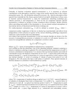
the method is valuable and highly appreciated.
As a result of the phase separation, islands of nano-crystalline silicon (Si-nc) embedded in a
SiO
2
matrix are obtained. Such a structure is shown in figure 31, using a TEM spectrum
(Inokuma et al., 1998). As it was proved in this section, this new material can be obtained
from silicon sub-oxides SiO
x
(0<x<2) as predecessors, and special post-deposition
treatments.
Fig. 31. Islands of Si nano-crystals embedded into a see of SiO
2
material. This new
material was obtained from SiO
1.3
annealed at 1100 C. The dimension and the
concentrations of these nano crystals are very important for applications in
optoelectronics. Reprinted with permission from Inokuma et al., 1998; copyright 1998,
American Institute of Physics.
Optoelectronics - Materials and Techniques
90
7.2 Phase separation induced by UV photons irradiation
Besides annealing and ion bombardment, another post deposition technique based on laser
irradiation of the SiO
x
thin films has been proposed to study the phase separation process
(Tomozeiu, 2006). This technique has been successfully utilized to change the structure of
the various amorphous materials (carbon nitride (Zhang and Nakayama, 1997) or
amorphous silicon (Aichmayr et al., 1998)). Thin films of various SiO
x
compositions have
been irradiated with different fluxes of UV laser photons (λ=274 nm).
In figure 32 are shown the IR spectra of the as deposited samples and of the laser irradiated
samples with various amount of UV photons. The peak position of the IR stretching
vibration mode measured on irradiated samples is shifted towards higher wave-number
values. For a better understanding, we mention the peak position for sputter deposited SiO
2
at 1054 cm
-1
(Tomozeiu, 2002). The as deposited SiO
1.2
samples are characterized by a peak
position at 1027.7 cm
-1
.
After the laser irradiation, the main peak has its maximum at 1068.2
cm
-1
,
when the laser energy is 55 mJ (which means 103.4 mJ/mm
2
). The full width at half-
maximum (FWHM) - an indicator of the structural homogeneity – was also changed by UV
irradiation. For the as deposited sample, the width of the peak was found 146.4 cm
-1
and for
the UV irradiated sample 106.1 cm
-1
( 55 mJ).
800 900 1000 1100 1200 1300
0.0
0.2
0.4
0.6
0.8
1.0
Normalized Si-O-Si IR peak
wavenumber (cm
-1
)
as deposited
Laser energy= 7.6mJ
10.3
19.3
25.8
30.8
37.3
55.0
72.1
Fig. 32. The normalized IR absorption spectra of the stretching vibration mode for as deposited
(full line) and UV irradiated samples with various laser energy (symbols). The energy
delivered during the laser treatment is a measure of the number of the incident photons
Other issues related to the changing of the peak shape are:
i.
the IR spectra of the laser treated samples have the main peak placed nearer the peak
position of the thermally grown SiO
2,
1073 cm
-1
(red shifted in comparison with the
sputter deposited SiO
2
;
ii.
the spectrum of the irradiated sample has a shoulder at 1250 cm
-1
that is specific to the
SiO
2
structure;
iii.
the shift in the peak position is dependent on the energy transferred to the SiO
x
via
photon impacts.
Generally, the shift in the peak position and the changes in the peak shape show the
structural changes in material. Figure 33 reveals the shift in the peak position and its
dependence on the incident photons’ energy.
Silicon Oxide (SiO
x
, 0<x<2): A Challenging Material for Optoelectronics
91
0 20 40 60 80 100 120 140
1020
1030
1040
1050
1060
1070
IR peak position (cm
-1
)
Laser energy density (mJ/mm
2
)
Fig. 33. The shift of the peak position assigned to the Si-O-Si stretching oscillation mode
with increasing the UV photon’s energy.
Considering the conservation of the silicon and oxygen atoms into the samples, the phase
separation revealed by IR peak position in the figures 30 and 33 can be equated as:
x2
xx
SiO SiO 1 Si
22
⎛⎞
→+−
⎜⎟
⎝⎠
(30a)
with intermediary steps, depending on the incident energy:
xxy
xx
SiO SiO 1 Si
xy xy
+
⎛⎞
→+−
⎜⎟
⎜⎟
++
⎝⎠
(30b)
The peak shape is drastically changed when more energy is added in the layer, especially
when the corresponding value of the SiO
x
dissociation energy is exceeded. Having a
calibration curve IR peak position versus oxygen content for 0<x<2 (see the section 3), the
value of the y parameter can be calculated. In this way, the formation of oxygen rich regions
in SiO
x
can be revealed.
What about the silicon islands? Spectroscopically, they can be emphasized with Raman
spectroscopy. For amorphous silicon the Raman signature is a wide peak centered on 480
cm
-1
. If the material is crystalline, the Raman spectrum has a very sharp peak (Hayashi and
Yamamoto, 1996) at 520 cm
-1
. Figure 34 shows the Raman spectra of SiO
1.2
as deposited and
laser treated samples. Increasing the laser energy, the peak centered at 480 cm
-1
increases in
intensity. This means that the amount of Si–Si bonds has been increased by the UV photon
irradiation.
Therefore, IR spectroscopy revealed the increasing of the Si-O bonds' number and the
Raman investigations showed the increase of the Si-Si number when the SiO
x
sample has
been laser irradiated. Increasing the energy delivered to the material, more oxygen-rich and
silicon-rich material has been detected. Increasing more the energy delivered to the SiO
x
it is
possible to induce the phase separation (silicon and SiO
2
) together with the phase
transformation: from amorphous into crystalline silicon. The sharp peak centered on 520 cm
-1
,
which is the fingerprint for crystalline silicon, increases in intensity with increasing the
Optoelectronics - Materials and Techniques
92
energy above a certain threshold value. Fitting the Raman spectrum with two gaussians –
one for amorphous phase and the other for crystalline phase – the amount of the silicon
transformed in crystalline silicon can be evaluated: 15.9% and 28.3% for incident UV energy
of 70.1 mJ/mm
2
and 103.4 mJ/mm
2
, respectively. This proves the possibilities of the
method to obtain Si-nc embedded into SiO
2
matrix.
400 450 500 550
0
1000
2000
3000
4000
Raman intensity (a.u.)
Wavenumber (cm
-1
)
as dep.
las. 19.4 mJ/mm
2
46.5
70.1
103.4
Fig. 34. The Raman spectra provide information regarding the increasing of Si-Si bonds
when the photons’ energy increases. The spectra of the samples irradiated with 70.1 and
103.4 mJ/mm
2
show the development of crystalline silicon from amorphous phase.
Also, the EPR measurements made on as-deposited and laser-treated samples, have revealed
changes in the type of the structural defects. It was seen that, increasing the number of the
incident photons, the amount of D
0
defect-like increases. Taking into account the influence of
these defects on electrical conductivity, on capturing and trapping the electrical carriers and
from here on the recombination electron-hole mechanisms, a real picture on the phase
separation and its applicability in optoelectronics can be penciled. Such new materials as Si-nc
embedded into a SiO
2
matrix (ore other dielectric matrix) are intensively studied and much
required for silicon based light emitters in integrated optoelectronics.
7.3 Applications in optoelectronics
The Light Emitting Diodes (LED-s) represent together with the laser diodes the photonic
devices that convert electrical energy into optical radiation. In the last half century the needs
for such devices increased exponentially; new research sectors and industries have been
developed due to these light producing devices. Optoelectronics, optronics and integrated
optics have been developed and gained an important place in our daily life. However, as it
is well known, silicon as material utilized in microelectronics devices is a poor light emitting
material because of its indirect band-gap. But, silicon nano-crystals offer a solution because
of their tunable indirect band-gap and more efficient electron-hole recombination. This is
why, the discovery of visible light emission from silicon nano-structures has stimulated
great interest for both the theoretical studies to understand the emission mechanisms, and
the experimental approaches to obtain these nano-crystals. Also, the integration of such light
sources within the optoelectronic devices is highly desirable.
Silicon Oxide (SiO
x
, 0<x<2): A Challenging Material for Optoelectronics
93
As general knowledge, we note that the luminescence is the emission of an optical radiation
due to the electronic excitation within a material. In LED the excitation of the carriers is the
result of the electrical field or the current over/through the device. The photons’ emission is
the result of the recombination processes, which are favored by the creation of non-
equilibrium states where the density of the minority carriers becomes much larger than the
value corresponding to the equilibrium. We also note that within solid state devices, there
are non-radiative recombination mechanisms that will reduce (cancel) the efficiency of the
radiative ones.
Silicon nanocrystals can be considered low-dimensional structures with size of few
nanometers. The structure of the electronic density of states is dramatically changed when
theoretically we pass from three dimensional structures to one- or zero- dimensional
structures. When the nanocrystals are structures with size comparable to the exciton Bohr
radius (1-3 nm), the confinement induces a localization of the produced exciton. In many
publications, the proposed model for the luminescence mechanisms is based on quantum
confinement effects in silicon nano-crystals embedded in SiO
2
or other dielectric materials.
The transition between the Si-nc and the SiO
2
matrix is a region with dangling bonds defects
which appears because of the mismatch in the structural lattice of the two materials. These
defects act as traps for the electrons and/or holes and, as a consequence, they quench the
luminescence. Their passivation by hydrogen or oxygen atoms have been proved as being
effective. According to the quantum confinement effect model, the photoluminescence in
visible is observed when the band-gap of the nano-silicon is large enough due to the size
reduction of the silicon nano-crystals. This together with a very well passivated surface by
Si-H or Si-O bonds are the ingredients for a high efficiency in light emission from silicon
nano-crystals embedded in SiO
2
.
We mention that some publications suggest that surface states at the interface between the
Si-nc and the composition of this intermediate layer are the principal mechanisms leading to
photoluminescence Koch et al., 1993). This model opened a new perspective on approaching
the emission mechanisms. Moreover, in some situations researchers invoked both models to
explain the photoemissions on two different optical wavelength ranges: the emitted light at
1.8-2.1 eV is explained via the quantum confinement effects, while the band at 2.55 eV is
related to localized surface states at the SiO
x
/Si interface (Chen et al., 2003).
Without getting into the details of these models (this is not the purpose of this work) we
consider necessary to discuss two issues: a) the influence of the nanocrystals’ size on the
light emission, and b) the light amplification in silicon nanocrystals.
Concerning the first subject, the spatial dimension of the silicon nanocrystals is the key
factor in tuning the electronic density of states in silicon and, in the theory of the quantum
confinement. Moreover the size of the nano-crystals is important in obtaining the right
emission spectrum. This is revealed in figure 35 where the peak maximum of the
photoluminescence is plotted against the mean crystal size according. The data are from
literature (Inokuma et al, 1998; Kahler and Hofmeister, 2002) and reveal the
photoluminescence (PL) spectra in SiO
x
films subjected to thermal annealing between 750
0
C
and 1100
0
C.
This study shows that there is a remarkable increase in the PL intensity after annealing at
temperature above 1000
0
C. Both, the composition of the as-deposited SiO
x
and the annealing
temperature value play an important role in the dimension of the crystals and, from here on
the photoluminescence spectrum. Depending on the deposition method for the SiO
x
precursor thin film and on the post-deposition treatment in order to obtain the phase
Optoelectronics - Materials and Techniques
94
separation, the silicon nanocrystals result in different sizes. The higher is the annealing
temperature, the larger are the obtained nano-crystals. From the data plotted in figure 35, a
correlation between the PL peak and the mean crystal size can be penciled:
() ()
PL max
nm 77.53 mean cryst. size nm 552.6λ=⋅ +
(31)
2.4 2.8 3.2 3.6 4.0 4.4
760
780
800
820
840
860
880
Inokuma et al, 1998
Kahler & Hofmeister, 2002
PL peak (nm)
Mean crystal size (nm)
y=77.53 x+552.6
Fig. 35. The size of the silicon nanocrystals does matter in the light emission. This experimental
data from literature show the importance of the post-deposition annealing in PL.
We mention that this relation was obtained from studies of SiO
x
samples post-deposition
annealed. Concerning the issue of silicon nanocrystals as light amplification, this is a step
further from LED towards the laser diode. The works of Pavesi et al (e.g. Pavesi et al, 2000)
have already penciled the main model for this new function of the silicon nanocrystals
embedded into SiO
2
matrix. Their energy diagram for a nano-crystal that works in
lightemission regime represents a pioneering work in this field. The diagram consists of
three energy levels, where two are the HOMO and LUMO nano-crystal bands’ edges and
the third level is an instable energy level placed into the band-gap region (between LUMO
and HOMO levels). Let it to be called inversion level. Via an external pumping mechanism
the electrons are transferred from the valence band edge (HOMO level) to the conduction
band edge (LUMO level) and from here, via a fast transition (time-scale of 10
-9
s) the
electrons will populate the inversion level. This is an instable energy level and the electrons
will radiatively recombine with the holes from the valence band. This schematic energy
diagram (see figure 7 of Pavesi et al., 2000) shows how the stimulated emission can be
obtained from silicon nano-crystals embedded into SiO
2
. More work is in course and we are
confident that the laser light obtained from silicon-based materials, compatible with the
silicon technology will be a reality in the nearest future.
In the last years, solar cells research and production have been much revigorated. Silicon
based solar cells (mono-crystalline and amorphous) are the main candidates for this
industry. The efficiency of a solar cell is defined by the carriers’ generation per incoming
photon. For photons with energy larger that the optical band-gap, it is considered that one
pair of electron hole is generated by one photon. In 2000 a group of researchers at National
Renewable Energy Laboratory (NREL) has found hat solar cells made with silicon
nanocrystals could produce several electrons from one photon from the UV part of the
Silicon Oxide (SiO
x
, 0<x<2): A Challenging Material for Optoelectronics
95
sunlight. The mechanism proposed was called “multiple exciton generation” and the
calculations showed that these nanocrystals theoretically convert more than 40% of the light
energy into electrical power. In a typical solar cell the energy in blue and UV light serves to
produce one electron and the rest is transformed in heat. When silicon nanocrystals are used
as solar cells material, this “lost” energy is converted via quantum-mechanical effects using
the multiple exciton generation processes into electrons (Bullis, 2007). Although this
technology is at the beginning, it is considered as the main step in obtaining a super efficient
solar cell and studies are made in collecting these new generated electrons with a short
lifetime.
Silicon nanocrystals are seen as promising biophotonics materials (Li and Ruckenstein, 2004;
Michalet et al., 2005). In fact they can be used as luminescent markers for biological samples,
having a low level of toxicity. Of great interest it is now the surface passivation of the water-
dispersed Si-nc with organic compounds; in this way the luminescence is stabilized and
their function as markers is more accurate. Moreover, considering the high surface-to-
volume ratio of these nanocrystals, another function for them is foreseen: as therapeutic and
diagnostic (theranostic) agent (Ho and Leong, 2010). There many conditions that an
inorganic nanocrystal must accomplish for a complete compatibility with the in vivo organic
material. According to this mini-review paper, the quantum dots have become a widely
used research tool for diagnostics, cell and molecular biology studies and in vivo
bioimaging. We mention that the authors have discussed only about the nano-particles as 5-
50 nm of A
2
B
6
(e.g. CdTe and CdSe) and A
3
B
5
(e.g. InAs and InP) group of materials. A
problem that must be solved is related to the toxicity of these elements for the living cell. It
seems that the silicon nanocrystals are characterized by a low toxicity level and their use for
these applications is in study.
As it was seen from this section the applications for the silicon nanocrystals embedded into
a dielectric matrix are multiple and very actual. A better understanding of the processes that
enable their formation and growth, and of their role within an optoelectronic (of
biophotonic) application will end up into a high quality and more efficient devices.
8. Acknowledgements
The author is grateful to the group headed by Prof. Dr. FHPM Habraken from Utrecht
University for support and interesting discussions. The permanent support offered by R&D
Océ Technologies B.V. is acknowledged.
9. References
Aichmayr, G.; Toet, D.; Mulato, M.; Santos, P.V.; Spangenberg, A.; Christiansen, S.; Albrecht,
M. & Strunk, H.P., (1998), Lateral grain growth during the laser interference
crystrallization of a-Si, Phys. Status Solidi, A166, pp. 659 - 666.
Arnoldbik, W.M.; Tomozeiu, N.; van Hattum, E.D.; Lof, R.W.; Vredenberg,
A.M. &
Habraken,
F.H.P.M., (2005), High-energy ion-beam-induced phase separation in SiO
x
films, Phys. Rev. B71, pp. 125329-125336
Ashcroft , N.W. & Mermin, N.D. (1988). Solid State Physics, ISBN0-03-049346-3, ch. 17
Brottger, H. & Bryksin, V.V. (1985). Hopping conduction in solids, Akademie-Verlag Berlin,
ISBN-10 -
0895734818, pp. 236
Bullis, K. (2007), Silicon Nanocrystals for Superefficient Solar Cells paper published on 15
Optoelectronics - Materials and Techniques
96
Augusts 2007, in
Carrier, P;. Abramovici, G.; Lewis, L.J. & Dharma-Wardana, M.W.C. (2001). Electronic and
Optical Properties of Si/SiO
2
Superlattices from First Principles : Role of Interfaces. Mat.
Res. Soc. Symp. Proc. vol. 677, pp. AA4.10.1 - AA4.10.6
Carrier, P.; Lewis, L.J. & Dharma-Wardana, M.W.C. (2002). Optical properties of structurally
relaxed Si/SiO
2
superlattices: The role of bonding at interfaces, Phys. Rev. B65, pp.
165339-165350
Chen, X.Y.; Lu, Y.F.; Wu, Y.H.; Cho, B.J.; Liu, M.H.; Dai, D.Y. & Song, W.D. (2003), Laser
annealing of silicon nanocrystal films prepared by pulsed-laser deposition, J. of Appl.
Phys. 93, no.10, pp. 6311 - 6316
Cho, K.S.; Park, N-M.; Kim, T-Y.; Kim, K-H.; Sung, G. Y. & Shin, J. H. (2005), High effieciency
visible electroluminescence from silicon nanocrystals embedded in silicon nitride using a
transparent doping layer, Appl. Phys. Lett. 86, pp.909-071911
Cody, G. D.; Tiedje, T.; Abeles, B.; Brooks, B. & Goldstein, Y. (1981). Disorder and the Optical-
Absorption Edge of Hydrogenated Amorphous Silicon, Phys. Rev. Lett. 47, pp. 1480-
1483
Cullis, A.G. & Canham, L.T. (1991). Visible light emission due to quantum size effects in highly
porous crystalline silicon, Nature 353 pp. 335-338
Gibbs, G.V.; Boisen, M.B.; Hill, F.C.; Tamada, O. & Downs, R.T. (1998). SiO and GeO bonded
interactions as inferred from the bond critical point properties of electron density
distributions, Phys Chem Minerals 25, 574-584
Hamann, D.R., (2000), Energetics of silicon suboxides, Phys. Rev., B61 pp.9899-9901
Hayashi, S. & Yamamoto, K. (1996) Optical properties of Si-rich SiO
2
films in relation with
embedded Si mesoscopic particles, J. Lumin. 70 no. 1-6, pp. 352 - 363.
Hinds, B.; Wang, F.; Wolfe, D.; Hinkle, C. & Lucovsky, G. (1998), Investigation of postoxidation
thermal treatments of Si/SiO
2
interface in relationship to the kinetics of amorphous Si
suboxide decomposition, J. Vac. Sci. Technol. B16, pp. 2171-2177
Ho, Y.P. & Leong, K.W. (2010), Quantum dot-based theranostics, Nanoscale, 2, pp. 60 -68
Hutchings, D.C.; Sheik-Bahae, M.; Hagan, D.J. & van Stryland, E.W. (1992). Kramers-Kronig
Relations in Nonlinear Optics, Optical and Quantum Electronics 24 , pp. 1-30 (and the
first two references of this paper)
Inokuma, T.; Wakayama, Y.; Muramoto, T.; Aoki, R.; Kurata, Y. & Hasegawa, S. (1998),
Optical properties of Si clusters and Si nanocrystallites in high-temperature annealed SiOx
films, J.of Appl. Phys. 83, nr 4, pp. 2228 - 2234
Kahler U. & Hofmeister, H. (2002), Size evolution of silicon nanocrystallites in evaporated thin
films of SiO
x
upon thermal processing, Appl. Phys. A74, pp. 13 - 17
Knights, J.C.; Street, R.A. & Lucovsky, G. (1980). Electronic and structural properties of plasma-
deposited a-Si:O:H - The story of O
2
, J. Non-Cryst. Solids, 35-36 pp. 279 - 284
Koch, F.; Petrova-Koch, V. & Muschik, T. (1993), The luminescence of porous Si: the case for the
surface state mechanism, J. of Luminescence 57, pp. 271 - 281
Li, Z.F. & Ruckenstein, E. (2004), Water-soluble poly(acrylic acid) grafted luminescent
silicon nanoparticles and their use as fluorescent biological staining labels , Nano
Letters, 4, no. 8, pp. 1463 -1467
Lu, Z.H.; Lockwood, D.J. & Baribeau, J.M. (1995). Quantum confinement and light emission in
SiO
2
/Si superlattices, Nature 378, pp. 258-260
Lucovsky, G. & Pollard, W.B. (1983). Local bonding of oxygen and hydrogen in a-Si:H:O thin
films, J. Vac. Sci. Technol. A 1, pp. 313 - 317
Silicon Oxide (SiO
x
, 0<x<2): A Challenging Material for Optoelectronics
97
Madan, A. & Shaw, M. (1988). The physics and applications of amorphous semiconductors,
Academic Press Inc. ISBN-10: 9780124649606
Michalet, X.; Pinaud, F.F.; Bentolila, L.A.; Tsay, J.M.; Doose, S.; Li, J.J.; Sundaresan, G.; Wu,
A.M.; Gambhir,S.S. & Weiss, S. (2005), Quantum Dots for Live Cells, in Vivo Imaging,
and Diagnostics, Science, 307, no 5709, pp. 538-544
Morimoto, A.; Nariyama, H. & Shimizu ,T. (1987). Structure and Defects in Amorphous Si–O
Films, Jap. J. of Applied Phys. 26, no. 1, pp. 22-27
Mott, N.F. & Davis, E.A. (1979). Electronic processes in non-crystalline materials, Oxford
University Press, second edition, ch 2
Nassiopoulos, A.G.; Grigoropoulos, S. & Papadimitriou, D. (1996). Electroluminescent device
based on silicon nanopilars, Appl. Phys. Lett. 69, pp. 2267-2269
O’Leary, S.K.; Johnson, S.R. & Lim, P.K. (1997). The relationship between the distribution of
electronic states and the optical absorption spectrum of an amorphous semiconductor: An
empirical analysis, J. Appl. Phys., 82, no 7, pp. 3334 - 3341
Pai, P.G.; Chao, S.S.; Takagi, Y. & Lucovsky, G. (1986). Infrared spectroscopic study of SiOx
films produced by plasma enhanced chemical vapor deposition, J. Vac. Sci. Technol. A 4
(3), pp. 689-695
Pavesi, L.; Dal Negro, L;. Mazzoleni, C.; Franzo, G.& Priolo, F. (2000). Optical gain in silicon
nanocrystals, Nature 408, pp. 440-444
Pollak, M. & Reiss, I. (1976). A percolation treatment of high-field hopping transport , J.
Phys. C 9 pp. 2339 - 2352
Puzder, A.; Williamson, A. J.; Crossman, J. C.; & Galli, G. (2002). Surface Chemistry of Silicon
Nanoclusters, Phys. Rev. Lett. 88, pp. 097401 - 04
Ravindra, N.M.; Auluck, S. & Srivastava, V. K. (1979). On the Penn gap in semiconductors,
Phy. Stat. Sol B 93, no. 2, pp. K155 - K160
Singh, A.; Bayliss, S.C.; Gurman, S.J. & Davis, E.A. (1992), The amorphous SiO
x
: H
y
thin film
system. III. Structure and bonding, J. Non-Cryst. Solids 142, pp. 113 - 125
Stolze, F.; Zacharias, M.; Schippel, S. & Garke, B. (1993). Compositional investigation of
sputtered amorphous SiOX:H, Solid State Communications, 87, no. 9 pp. 805-808
Street, R.A. (1991). Hydrogenated amorphous silicon, Cambridge University Press, ch. 4.
Tauc, J.; Grigorovici, R. & Vancu, A. (1966). Optical Properties and Electronic Structure of
Amorphous Germanium, Phys. Stat. Sol. 15, pp. 627- 637
Theiss,W. (2002). Scout program in
Tomozeiu, N.; van Hapert, J.J.; van Faassen, E.E.; Arnoldbik, W.M.; Vredenberg, A.M. &
Habraken, F. H. P. M. (2002), Structural properties of a-SiOx layers deposited by
reactive sputtereing technique, J. of Optoelectronics and Advance Materials, 4, no. 3,
pp. 513 - 521
Tomozeiu, N.; van Faassen, E.E.; Habraken, F.H.P.M. (2003). Structural transition in silicon
suboxides at critical oxygen content, Annals of West University of Timisoara, Series
Chemistry 12, no. 3, pp 1039 - 1046
Tomozeiu, N. (2006), Effects of UV photon irradiation on SiOx (0<x<2) structural properties,
Applied Surface Science 253, pp. 376–380
Tomozeiu, N. (2006). SiOx, thin films deposited by rf magnetron reactive sputtering: structural
properties designed by deposition conditions, J. of Optoelectronics and Advance
Material, 8, no. 2 pp. 769 -775
Optoelectronics - Materials and Techniques
98
van Hapert, J.J. (2002). Hopping conduction and chemical structure - a study on silicon suboxides,
PhD Thesis, Utrecht University ISBN 90-393-3063-8, ch 3 and 4
van Hapert, J.J.; Vredenberg, A.M.; van Faassen, E.E.; Tomozeiu, N.; Arnoldbik, W.M. &
Habraken, F. H. P. M., (2004), Role of spinodal decomposition in the structure of SiOx ,
Phys. Rev. B 69 pp. 245202-245210
Zacharias, M.; Drusedau, T.; Panckow, A.; Freistedt, H. & Garke, B. (1994). Physical properties
of a-SiOx : H alloys prepared by dc magnetron sputtering with water vapour as oxygen
source, J. of Non-Crystalline Solids 169, pp. 29-36
Zhang, M. & Nakayama, Y. (1997), Effect of Ultraviolet Light lrradiation on Amorphous Carbon
Nitride Films, J. Appl. Phys. 82, no. 10, pp. 4912- 4015.
Zhang, R. Q.; Chu, T. S.; Cheung, H. F.; Wang, N. & Lee, S. T. (2001). High reactivity of silicon
suboxide clusters, Phys. Rev. B64, pp. 113304 - 113308
Zhang, R. Q.; Lee, C. S. & Lee, S. T. (2001). The electronic structures and properties of Alq3
and NPB molecules in organic light emitting devices: decompositions of density of
states J. Chem. Phys. 112, pp. 8614-8620
Weast, R.C. (1968). editor of Handbook of Chemistry and Physics, the 48-th edition, The
Chemical Rubber Publishing Co., F149
Wilson, W.L.; Szajowski, P.F. & Brus, L.E. (1993). Quantum Confinement in Size-Selected,
Surface-Oxidized Silicon Nanocrystals, Science 262, pp. 1242-1244
Wolkin, M.V.; Jorne, J.; Fauchet, P.M. Allan, G. & Delerue, C. (1999). Electronic states and
luminiscence in porous silicon quantum dots, Phys. Rev. Lett. 82, pp. 197-200
4
Gallium Nitride: An Overview of
Structural Defects
Fong Kwong Yam, Li Li Low, Sue Ann Oh and Zainuriah Hassan
School of Physics, Universiti Sains Malaysia,
Malaysia
1. Introduction
1.1 Foreword
The III-V nitrides have long been viewed as promising semiconductor materials for their
application in the blue and ultraviolet wavelengths optical devices, as well as high power
and high temperature electronic devices. In the absence of a suitable gallium nitride (GaN)
substrate, GaN, and related III-V materials are heteroepitaxially grown on sapphire or other
substrates. GaN grown on sapphire normally contains a high density of threading
dislocations in the range of 10
10
cm
-2
(Lester, 1995; Qian, 1995a; Hong & Cho, 2009) due to
lattice constant and thermal expansion coefficient mismatches between GaN and sapphire.
Besides threading dislocations, there are many other structural defects, such as, inversion
domain, stacking mismatch boundaries, micropipes/nanopipes or voids, and surface pits.
These defects will cause the periodicity of the crystal to be disrupted over distances of
several atomic diameters from the defect and affect the optoelectronic properties of the
devices. For example, threading dislocations have been found to act as nonradiative centers
and scattering centers in electron transport that is detrimental to the performance of light
emitting diodes and field-effect transistor (Ng et al., 1998). Dislocations defects cause rapid
recombination of holes with electrons without conversion of their available energy into
photons, i.e., nonradiative recombination, which causes heating up of the crystal and
making optoelectronic devices malfunction (Hong & Cho, 2009; Garni et al., 1996). With the
advancement of crystal growth technology, crystal defects in GaN have been reduced
tremendously. The threading dislocations density in the GaN films has been reduced from
the range of 10
10
cm
-2
to 10
5
cm
-2
. However, effort to further reduce the density of structural
defects in GaN is strongly driven by the growth of high crystal quality thin films for
fabrication of high performance optoelectronic devices.
1.2 The properties of GaN
Table 1 summarizes some of the most important properties of GaN. GaN shows many others
superior properties compared to other semiconductor materials, such as high breakdown field
of approximately 5×10
6
V/cm as compared to 3×10
5
and 4×10
5
V/cm for silicon (Si) and
gallium arsenide (GaAs) (Morkoc et al., 1994). GaN is also a very stable compound. Its
chemical stability at elevated temperatures coupled with wide bandgap has made GaN an
attractive material for device operation in high temperature and caustic environments.
Optoelectronics - Materials and Techniques
100
Wurtzite GaN
Bandgap energy E
g
(200K) =3.39eV; Eg(1.6K) = 3.50eV
Temperature coefficient dE
g
/(dT) = -6.0×10
-4
eV/K
Pressure coefficient dE
g
/(dP) = 4.2×10
-3
eV/kbar
Lattice constant a = 3.189Å; c = 5.185Å
Thermal expansion Δa/a =5.59×10
-6
K; Δc/c =3.17×10
-6
K;
Thermal conductivity k =1.3 W/cm K
Index of refraction n(1 eV) = 2.33; n(3.38 eV) = 2.67
Dielectric constants e
0
=8.9; e
∞
=5.35
Zincblende GaN
Bandgap energy E
g
(330K) =3.2 - 3.3 eV
Lattice constant a =4.52Å
Index of refraction n (3 eV) = 2.9
Table 1. The properties of GaN (Edgar, 1994).
Fig. 1. The wurtzite crystal structure. The full circles are N, and open circles are Ga atoms.
Adapted from ref. (Edgar, 1994).
Fig. 2. The zincblende crystal structure. The full circles are N, and open circles are Ga
atoms. Adapted from ref. (Edgar, 1994).
Gallium Nitride: An Overview of Structural Defects
101
GaN can exist in 2 different structures, which are hexagonal wurtzite (α-GaN) as shown in
Fig. 1 and cubic zincblende (β-GaN) in Fig. 2 (Edgar, 1994). The former is the stable
structure whereas the latter is the metastable structure.
For other technical data, readers are advised to refer to references (Morkoc et al., 1999a;
Edgar & Liu, 2002; Parmer, 2008; Harima, 2002; Levinshtein et al., 2001; Nakamura &
Chichibu, 2000; Henini & Razeghi, 2005).
2. Crystal defects
2.1 General classification of defects
The formation of defects during growth is unavoidable and can be classified by their
dimensionality as (Spitsyn et al., 1993):
a. Zero-dimensional defects or point defects, which are associated with a single atomic site
(e.g. vacancies, interstitials and substitutional atoms).
b. One-dimensional defects or line defects, which are associated with a direction (e.g.
dislocations).
c. Two-dimensional defects or planar defects, which are associated with a plane or area
(e.g. grain boundaries, stacking faults, twins and inversion domain boundaries). Planar
defects refer to the boundary between two orderly regions of a crystal. In other words,
they are separate regions having different crystallographic orientations.
d. Three-dimensional defects or volume defects, which are associated with a volume (e.g.
voids, cracks and nanopipes)
2.1.1 Point defects
In general, there are three main types of point defects: vacancies, interstitials and
substitutional atoms.
An unoccupied regular crystal site is called a vacancy (Fig. 3). For a binary compound
semiconductor, vacancies can either be cation or anion vacancies.
If an atom which does not occupy a regular crystal site but a site between regular atoms, it is
called an interstitial impurity atom (Fig. 3). In order for an impurity atom to stay at an
interstitial site, it must have sufficiently low energy there. This will be satisfied for
interstitial sites which either have high local symmetry or which lie on a bond between two
atoms. The incorporation of impurity atoms on interstitial sites is especially likely when the
impurity atom deviates relatively strongly from the atoms of the host crystal.
However, interstitials may also come from atoms of the crystal itself. If a chemically
compatible atom of the crystal occupies an interstitial site rather than a regular one, a self-
interstitial is produced. For this type of point defect to develop in a crystal, there must be
enough space between the host atoms, i.e. the crystal should not be packed too densely.
When an impurity atom substitutes an atom of the host crystal (Fig. 3), it is referred to as a
substitutional impurity. In a binary compound semiconductor, the substitutional
incorporation occurs on the lattice site which corresponds to the most chemically similar of
the two atoms of the compound. Substitutional impurity can be introduced into the crystal
either intentionally (controlled doping) or unintentionally (contaminants). Examples of
common unintentional substitutional impurities in GaN are oxygen and carbon. Oxygen
occupies N sites. As for carbon, calculations show that carbon is an amphoteric impurity in
Optoelectronics - Materials and Techniques
102
GaN (Boguslavski et al., 1996) although however, the incorporation of carbon on nitrogen
sites is preferable since the formation energy is lower.
Fig. 3. Schematic representation of common point defects.
Substitution may also come from atoms of the crystal itself. In a binary semiconductor
which consists of two different chemical elements, an atom of the first may occupy a regular
site of the second, and vice versa. Such point defects are called antisite defects.
From the explanation above, it is apparent that point defects can be categorized as intrinsic
or extrinsic. Intrinsic point defects encompass vacancies, self-interstitials and antisites, since
they come from the crystal itself. Meanwhile extrinsic point defects, which involve foreign
atoms, comprise of substitutional, impurities and interstitial impurities.
2.1.2 Dislocations
Dislocations are defined as abrupt changes in the regular ordering of atoms along a
dislocation line in the solid. Dislocations are mostly due to misalignment of atoms or
presence of vacancies along a line. The interatomic bonds are significantly distorted only in
the immediate vicinity of the dislocation line called the dislocation core. Dislocations also
create small elastic deformations of the lattice at large distances that cause lattice distortion
centered around a line. They are characterized by the Burgers vector
b , which describes the
unit slip distance in terms of magnitude and direction. The classification for dislocations are
as follows:
1. Edge dislocation;
2. Screw dislocation; or
3. Mixed dislocation, which contains both edge and screw dislocation components.
An edge dislocation (Fig. 4(a)) may be described as an extra plane of atoms squeezed into a
part of the crystal lattice, resulting in that part of the lattice containing extra atoms and the
rest of the lattice containing the correct number of atoms. The part with extra atoms would
therefore be under compressive stresses, while the part with the correct number of atoms
would be under tensile stresses. In an edge dislocation, the Burgers vector is perpendicular
to the dislocation line. Screw dislocations (Fig. 4(b)) result when planes are displaced
relative to each other through shear. In this case, the Burgers vector is parallel to the
dislocation line (W.F. Smith, 1996). In real crystals, however, most dislocations have mixed
edge/screw character.
Gallium Nitride: An Overview of Structural Defects
103
Fig. 4. Schematic representation of (a) edge dislocation (b) screw dislocation.
2.1.3 Stacking faults
Stacking faults, as the name implies, are partial displacements which upset the regular
sequence in the stacking of lattice planes. For example, in the zinc blended packing
sequence, ABCABC , one of the lattice planes may be out of sequence due to a stacking
fault, and become ABABCABC The result is then a mixture of zinc blende and wurtzite
stacking.
In wurtzite structure, there are two types of stacking faults: basal stacking faults and
prismatic stacking faults. Basal stacking faults consists of intrinsic ( I
1
and I
2
) types and an
extrinsic ( E )type. They can be treated as thin layers of cubic stacking. I
1
, I
2
and E
correspond to 3 (e.g. ABC), 4 (e.g. ABCA) and 5 (e.g. ABCAB) bi-atomic layers of cubic
structure, respectively. Prismatic stacking faults form on prismatic {1210} planes with a
displacement vector of ½ [0111]. When the sample is viewed in cross-section along the [0 0
01] zone axis, prismatic stacking faults are seen as zig-zags formed on (2110) and (1210)
planes (Hull & Bacon, 1984). It was found that prismatic stacking faults terminate I
1
-type
basal stacking faults and therefore sometimes their presence can be beneficial. Star-rod
dislocations are expected at the intersection of prismatic stacking faults and basal stacking
faults when their displacement vectors are not equal. Theoretical calculations predict high
formation energy for prismatic stacking faults (Northrup, 1998) of about 30 times higher
than that calculated for I
2
basal stacking faults (Zakharov et al., 2005).
2.1.4 Stacking mismatch boundaries
Stacking mismatch boundaries originate at substrate/film interface. Stacking mismatch
boundaries are created by surface steps on substrates which cause nucleation and growth of
separate III-nitrides domains at different levels: stacking disorder must occur across the
domain boundaries. The formation of these domains is believed to account for the relaxation
of the large lattice and thermal mismatches between nitrides and substrate. These stacking
irregularities are also known as double positioning boundaries.