Solar Cells Silicon Wafer Based Technologies Part 8 pptx
Bạn đang xem bản rút gọn của tài liệu. Xem và tải ngay bản đầy đủ của tài liệu tại đây (1.77 MB, 25 trang )
Solar Cells – Silicon Wafer-Based Technologies
166
leading to an increase of SVR. In other words, SVR has the impact of enlarging band gap. At
the same transverse dimension, triangular SiNW has larger SVR than those of the
rectangular SiNW and hexagonal SiNW. As a result, its larger SVR induces the largest band
gap among those of the rectangular and hexagonal SiNWs and the strongest size
dependence. The bandgap values versus SVR of the SiNWs are shown in Fig. 28 (b). The
SVR effect on the bandgap of [110] SiNWs with any cross-sectional shape and area can be
described by a universal expression (Yao et al., 2008)
E
G
(eV)=1.28+0.37 x S (nm
-1
),
where S is the value of the SVR in unit of nm
-1
. The bandgap of SiNWs are usually difficult
to measure, but their transverse cross-sectional shape and dimension are easy to know, so it
is of significance to predict the bandgap values of SiNWs by using the above expression.
4.2.2 Optical reflection and absorption in SiNWs
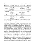
Si NW PV devices show improved optical characteristics compared to planar devices. Fig. 29
(a) shows typical optical reflectance spectra of SiNW film as compared to solid Si film of the
same thickness (~10m) (Tsakalakos et al., 2007a). As one can see, the reflectance of the
nanowire film is less than 5% over the majority of the spectrum from the UV to the near IR and
begins to increase at ~700°nm to a values of ~41% at the Si band edge (1100 nm), similar to the
bulk Si. It is clear that the nanowires impart a significant reduction of the reflectance compared
to the solid film. More striking is the fact that the transmission of the nanowire samples is also
significantly reduced for wavelength greater than ~700°nm (Fig. 29 (b)). This residual
absorption is attributed to strong IR light trapping
4
coupled with the presence of the surface
states on the nanowires that absorb below bandgap light. However, the level of optical
absorption does not change with passivation, which further indicates that light trapping plays
a dominant role in the enhanced absorption of the structures at all wavelength. It should be
also noted that the absorption edge of a nanowire film shifts to longer wavelength and
approaches the bulk value as the nanowire density is increased. Essentially, the Si nanowire
arrays act as sub-wavelength cylindrical scattering elements, with the mactroscopic optical
properties being dependent on nanowire pitch, length, and diameter.
Fig. 29. Total (a) reflectance and (b) transmission data from integrated sphere measurements
for 11 m thick solid Si film and nanowire film on glass substrate (Tsakalakos et al., 2007).
4
Light trapping is typically defined as the ratio of the effective path length for light rays confined
within a structure with respect to its thickness.
Silicon-Based Third Generation Photovoltaics
167
4.3 Electrical transport in SiNWs
Important factors that determine the transport properties of Si nanowires include the wire
diameter (important for both classical and quantum size effect), surface conditions, crystal
quality, and the crystallographic orientation along the wire axis (Ramayya et al., 2006)
(Duan et al., 2002).
Electronic transport phenomena in Si nanowires can be roughly divided into two categories:
ballistic transport and diffusive transport. Ballistic transport phenomena occur when the
electrons can travel across the nanowire without any scattering. In this case the conduction
is mainly determined by the contact between the nanowire and the external circuit. Ballistic
transport phenomena are usually observed in very short quantum wires. On the other hand,
for nanowires with length much larger than the carrier mean free path, the electrons (or
holes) undergo numerous scattering events when they travel along the wire. In this case, the
transport is in the diffusive regime, and the conduction is dominated by carrier scattering
within the wires, due to lattice vibrations, boundary scattering, lattice and other structural
defects and impurity atoms.
The electronic transport behavior of Si nanowires may be categorized based on the relative
magnitudes of three length scales: carriers mean free path, the de Broglie wavelength of
electrons, and the wire diameter. For wire diameters much larger than the carrier mean free
path, the nanowiers exhibit transport properties similar to bulk materials, which are
independent of the wire diameter, since the scattering due to the wire boundary is
negligible, compared to other scattering mechanisms. For wire diameters comparable or
smaller than the carrier mean free path, but still larger than the de Broglie wavelength of the
electrons, the transport in the nanowire is in the classical finite regime, where the band
structure of the nanowire is still similar to that of the bulk, while the scattering events at the
wire boundary alter their transport behavior. For wire diameters comparable to electronic
wavelength (de Broglie wavelength of electrons), the electronic density of states is altered
dramatically and quantum sub-bands are formed due to quantum confinement effect at the
wire boundary. In this regime, the transport properties are further influenced by the change
in the band structure. Therefore, transport properties for nanowires in the classical finite
size and quantum size regimes are highly diameter-dependent. Experimentally it was
shown that the carrier mobility in SiNWs can reach that one in bulk Si at a doping
concentration of 10
20
cm
-3
and decreases for smaller diameter wires (Cui et al., 2000).
Because of the enhanced surface-to-volume ratio of the nanowires, their transport behavior
may be modified by changing their surface conditions. For example, it was shown on the n-
InP nanowires, that coating of the surface of these nanowires with a layer of redox
molecules, the conductance may be changed by orders of magnitude (Duan et al., 2002).
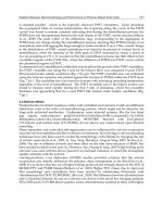
4.4 Comparison of axial and radial p-n junction nanowire solar cells
Independently of the nanowire preparation method two designs of NW solar cells are now
under consideration with p-n junction either radial or axial (Fig. 30). In the radial case the p-
n junction covers the whole outer cylindrical surface of the NWs. This was achieved either
by gas doping or by CVD deposition of a shell oppositely doped to the wire (Fang, 2008)
(Peng, 2005) (Tian 2007). In the axial variant, the p-n junction cuts the NW in two cylindrical
parts and require minimal processing steps (Andra 2008). However, solar cells that absorb
photons and collect charges along orthogonal directions meet the optimal relation between
the absorption values and minority charge carrier diffusion lengths (Fig. 30 (a)) (Hochbaum
2010). A solar cell consisting of arrays of radial p-n junction nanowires (Fig. 30 (b)) may
Solar Cells – Silicon Wafer-Based Technologies
168
provide a solution to this device design and optimization issue. A nanowire with a p-n
junction in the radial direction would enable a decoupling of the requirements for light
absorption and carrier extraction into orthogonal spatial directions. Each individual p-n
junction nanowire in the cell could be long in the direction of incident light, allowing for
optimal light absorption, but thin in another dimension, thereby allowing for effective
carrier collection.
(a)
(b)
Fig. 30. Schematic views of the (a) axial and (b) radial nanowire solar cell. Light penetration
into the cell is characterized by the optical thickness of the material ( is the absorption
coefficient), while the mean free path of generated minority carriers is given by their
diffusion length. In the case of axial nanowire solar cell, light penetrates deep into the cell,
but the electron-diffusion length is too short to allow the collection of all light-generated
carriers (Kayes et al., 2005).
The comparison between the axial and radial p-n junction technologies for solar cell
applications was performed in details in Ref (Kayes et al., 2005). In the case of radial p-n
junction, the short-circuit current (I
sc
) increases with the nanowire length and plateaus when
the length of the nanowire become much greater than the optical thickness of the material.
Also, I
sc
was essentially independent on the nanowire radius, provided that the radius (R)
was less than the minority carrier diffusion length (L
n
). However, it decreases steeply when
R > L
n
. I
sc
is essentially independent of trap density in the depletion region. Being rather
sensitive to a number of traps in the depletion region, the open circuit voltage V
oc
decreases
with increasing nanowire length, and increases with nanowire radius. On the other hand the
trap density in the quasineutral regions had relatively less effect on V
oc
. The optimal
nanowire dimensions are obtained when the nanowire has a radius approximately equal to
L
n
and a length that is determined by the specific tradeoff between the increase in I
sc
and the
decrease in V
oc
with length. In the case of low trap density in the depletion region, the
maximum efficiency is obtained for nanowires having a length approximately equal to the
optical thickness. For higher trap densities smaller nanowire lengths are optimal.
Radial p-n junction nanowire cells trend to favor high doping levels to produce high cell
efficiencies. High doping will lead to decreased charge-carrier mobility and a decreased
depletion region width, but in turn high doping advantageously increases the build-in
voltage. Because carriers can travel approximately one diffusion length through a
quasineutral region before recombining, making the nanowire radius approximately equal
Silicon-Based Third Generation Photovoltaics
169
to the minority –electron diffusion length allows carriers to traverse the cell even if the
diffusion length is low, provided that the trap density is relatively low in the depletion
region.
An optimally designed radial p-n junction nanowire cell should be doped as high as
possible in both n- and p- type regions, have a narrow emitter width, have a radius
approximately equal to the diffusion length of the electrons in the p-type core, and have a
length approximately equal to the thickness of the material. It is crucial that the trap density
near the p-n junction is relatively low. Therefore one would prefer to use doping
mechanisms that will getter impurities away from the junction. By exploiting the radial p-n
junction nanowire geometry, extremely large efficiency gains up to 11% are possible to be
obtained.
4.5 Fabrication of Si QD PV devices
By using VLS method (Tian et al., 2007) (Kelzenberg et al., 2008) (Rout et al., 2008) (Fang et
al., 2008) (Perraud et al., 2009) as well as by the etching method (Garnett et al., 2008) (Peng et
al., 2005). SiNW based photovoltaic devices were experimentally demonstrated. Nearly all
the works were concerned with Si wafers as a substrate. However, it should be noted that
for competitive solar cells, low cost substrates, such as glass or metal foils are to be
preferred. Schematic view of the VLS fabricated structure of the SiNW array solar cells is
illustrated on Fig. 31 (a). The n-type SiNWs were prepared by the VLS method on (100) p-
type Si substrate (14-22 cm). Device fabrication started from the evaporation of 2-nm thick
gold film followed by annealing at 550°C for 10 min under H
2
flow to form Au
nanocatalyzers. SiNWs were subsequently grown at 500° with SiH
4
diluted in H
2
as the gas
precursor. N-type doping was achieved by adding PH
3
to SiH
4
, with PH
3
/SiH
4
ratio of 2x10
-
3
corresponding to a nominal phosphorous density of 10
20
cm
-3
. After the VLS growth the
gold catalysts were etched off in KI/I
2
solution, and the doping impurities were activated by
rapid thermal annealing at 750° for 5 min. The SiNW array was then embedded into spin-
on-glass (SOG) matrix. Indeed, SOG matrix ensures a good mechanical stability of the SiNW
array and enables further processing steps, such as front surface planarization and electrical
contact deposition. The planarization step is normally performed by the chemical-
mechanical polishing. To form the front contacts indium-tin-oxide (ITO) was firstly
deposited on planarized SOG surface followed by the deposition of Ni/Al contact grid. As
back electrical contact, the sputtered and annealed Al was used. The area of the fabricated
SiNW solar cell was 2.3 cm
-2
.
The sheet resistance of n-type SiNWs embedded into SOG matrix was estimated to be 10
-4
/sq. I-V measurements in the dark and under 1-sun illumination (Fig. 31 (b)) indicate a
good rectifying junction. The measured I
SC
, V
OC
and FF were 17 mA/cm
2
, 250mV and
44%, respectively, leading to an energy-conversion efficiency of 1.9%. The V
OC
of Si NW
solar cell was shown to be increased up to 580 mV (Peng et al., 2005). The parasitic series
resistance found for SiNW solar cells (~5 cm
-2
) was slightly larger than in the standard
1
st
generation solar cells (~2 cm
-2
), however the p-n junction reverse current was of the
order of 1 A/cm
2
with is about 100 times bigger than in typical Si solar cells
(~1 pA/cm
2
). Such a high pn junction reverse current indicates a high density of localized
electronic states within the bandgap, which act as generation-recombination centers.
These states may come from contamination of Si by gold which is used as catalyst for VLS
growth. Other types of metallic catalysers, like Sn, were also used (Uchiyama et al., 2010).
Solar Cells – Silicon Wafer-Based Technologies
170
However, for a moment by using this catalyzer it is difficult to achieve the diameter of
SiNWs less that 200 nm. The electronic states in the bandgap may also come from a lack of
passivation of surface defects. The passivation step is rather crucial for SiNW solar cells,
since SiNW have very high SVR ratio and their opto-electronic properties strongly
depends on the surface passivation.
(a)
(b)
Fig. 31. (a) Structure of the SiNW array solar cell. A p-n junction is formed between the n-
type SiNWs and the p-type Si substrate; (b) Dark and illuminated I-V measurements of n-
type SiNWs on p-type Si substrate (Perraud et al., 2009).
The theoretical value of the efficiency for Si nanowire solar cells is predicted to be as high
as 16%, which makes them perfect candidates for higher bandgap bricks in all-Si tandem
cell approach. The first prototypes of SiNW solar cells have excellent antireflection
capabilities and shown the presence of the photovoltaic effect. However, up today there
was no evidence that this photovoltaic effect occurred in a material with an increased
bandgap.
5. Conclusions
Silicon based third generation photovoltaics is a quickly developing field, which integrates
the knowledge from material science and photovoltaics. Today the first prototypes of both
Si QD solar cells and Si NWs solar cells have already been developed. For a moment they
present V
OC
, I
SC
and FF values which still lower than those ones of the 1
st
generation PV cells
based on bulk Si – but all these problems are being addressed. It is too prematurely to draw
the conclusions while the further optimization steps of the fabrication parameters were not
performed. We should not forget that, for example, although the airplane was not invented
until the early 20
th
century, Leonardo da Vinci sketched a flying machine four centuries
earlier.
6. References
Abeles, B.; Pinch, H. L. & Gittleman, J. I. (1975), Percolation conductivity in W-Al
2
O
3
granular metal films, Phys. Rev. Lett., Vol. 35, pp. 247-250.
Aeberhard, U. (2011), Theory and simulation of photogeneration and transport in Si-SiOx
superlattice absorbers, Nanoscale Research Letters, Vol. 6, p. 242.
Silicon-Based Third Generation Photovoltaics
171
Allan, G. & Delerue, C. (2007), Energy transfer between semiconductor nanocrystals:
Validity of Förster’s theory, Phys. Rev. B, Vol. 75, pp. 195311.
Andra, G.; Pietsch, M.; Sivakov, V.; Stelzner, Th.; Gawlik, A.; Christiansen, S.& Falk, F.
(2008). Thin film solar cells based on single crystalline silicon nanowires,
Proceedings of 23
th
European Photovoltaic Solar Cell Energy Conference., Spain, pp. 163-
167
Antonova, A.; Gulaev, M.; Savir, E.; Jedrzejewski, J, & Balberg, I. (2008), Charge storage,
photoluminescence, and cluster statistics in ensembles of Si QDs, Phys. Rev. B., Vol.
77, pp. 123318.
Balberg, I,; Azulay, D.; Toker, D. & Millo, O. (2004), Percolation and tunneling in composite
materials, Int. J. Mod. Phys. B, Vol. 18, pp. 2091-2121.
Balberg, I.; Savir, E.; Jedrzejewski, J, Nassiopoulou, A. & Gardelis, S. (2007), Fundamental
transport processes in ensembles of silicon quantum dots, Phys. Rev. B., Vol. 75, pp.
235329.
Balberg, I. (2010) Chapter 4, in Silicon Nanocrystals: Fundamentals, Synthesis and Application
(ed. L. Pavesi and R; Turan), Wiley, Weinheim.
Ball, J. & Reehal, H. (2010), The effect of substrate bias on the growth of silicon nanowires
from Tin catalyst layers,, Proceedings of 25
th
European Photovoltaic Solar Cell Energy
Conference, Spain, September 6-10, pp. 769-772.
Bulutay,C. (2007), Electronic structure and optical properties of silicon nanocrystals along
their aggregation stages , Physica E, Vol. 38, pp. 112.
Bulutay, C. & Ossicini, S. (2010) Chapter 2, in Silicon Nanocrystals: Fundamentals, Synthesis
and Application (ed. L. Pavesi and R; Turan), Wiley, Weinheim.
Canham, L. T. (1990), Silicon quantum wire array fabrication by electrochemical and
chemical dissolution of wafers, Appl. Phys. Lett., Vol. 57, pp. 1046.
Cho, E-Ch,; Green, M.; Xia, J.; Corkish, R.; Reece, P.; & Gal, M (2004), Clear quantum-
confined luminescence from silicon/SiO
2
single quantum wells, Appl. Phys. Lett.,
Vol. 84, p. 2286.
Cho, Y. H.; Green, M. A.; Cho, E-Ch.; Huang, Yu.; Trupke, Th. & Conibeer, G. (2005), Silicon
quantum dots in SiNx matrix for third generation photovoltaics, Proceedings of 20
th
European Photovoltaic Solar Cell Energy Conference, Spain, June 6-10, pp. 47-50
Cho, E.C.; Green, M.A.; Conibeer, G.; Song, D.Y.; Cho, Y.H.; Scardera, G.; Huang, S.J.; Park,
S.; Hao, X.J.; Huang, Y. & Dao, L.V. (2007) Silicon quantum dots in a dielectric
matrix for all-silicon tandem solar cells. Adv. OptoElectr., 2007, Article ID 69578.
Conibeer, G.; Green, M.; Cho, Cho, Eu-Ch.; König, D.; Cho, Y-H.; Fangsuwannarak, T.;
Scardera, G.; Pink, E.; Huang, Yi.; Puzzer, T.; Huang, Sh.; Song, D.; Flynn, Ch.;
Park, S.; Hao, X.& Mansfield, D. (2008), Silicon quantum dot nanostructures for
tandem photovoltaic cells, Thin Solid Films, Vol. 516, pp. 6748-6756.
Conibeer, G. (2010) Chapter 20, in Silicon Nanocrystals: Fundamentals, Synthesis and
Application (ed. L. Pavesi and R; Turan), Wiley, Weinheim.
Conibeer, G.; Green, M.; König, D.; Perez-Wurfl, I.; Huang, S.; Hao, X.; Di, D.; Shi, L.;
Shrestha, S.; Puthen-Veetil, B.; So, Y.; Zhang, B. & Wan, Z. (2010a), Silicon quantum
dot based solar cells: addressing the issues of doping, voltage and current
Solar Cells – Silicon Wafer-Based Technologies
172
transport, Proceedings of 25
th
European Photovoltaic Solar Cell Energy Conference, Spain,
September 6-10, pp. 182-190.
Crisp, D.; Pathare, A. & Ewell, R.C. (2004), The performance of gallium
arsenide/germanium solar cells at the Martian surface, Acta Astronautica, Vol. 54,
pp. 83-101.
Cui, Y.; Duan, X.; Hu, J. & Lieber, C.M., (2000), Doping and electrical transport in Si
nanowires, J. Phys. Chem. B Vol. 104, pp. 5213-5216.
Cui Y., & Lieber, C.M. (2001), Functional Nanoscale Electronic Devices Assembled Using
Silicon Nanowire Building Blocks, Science Vol. 291, pp. 851-853.
Cui, Y.; Lauhon, L.J.; Gudiksen, M.S.; Wang J. & Lieber, C.M. (2001a), Diameter-controlled
synthesis of single-crystal silicon nanowires, Appl. Phys. Lett. Vol. 78, pp. 2214
Degoli, E.; Luppi, M. & Ossicini, S. (2000), From Undulating Si Quantum Wires to Si
Quantum Dots: A Model for Porous Silicon, Phys. Stat. Solidi (a), Vol. 182, pp. 301
Di. D.; Perez-Wurfl, I.; Conibeer, G. & Green, M. (2010) Formation and photoluminescence
of Si quantum dots in SiO
2
/Si
3
N
4
hybrid matrix for all-Si tandem solar cells, Sol.
Energy Mater. Sol. Cells. Vol. 94, pp. 2238-2243.
Duan, X.; Huang, Y. & Lieber, C. (2002) Nonvolatile memory and programmable logic from
molecule-gated nanowires, Nano Lett., Vol. 2, pp. 487-490.
Erwin, S.C.; Zu, L.J.; Haftel, M.I.; Efros, A.L.; Kennedy, T.A.; & Norris, D.J. (2005) Doping
semiconductor nanocrystals. Nature, Vol. 436, pp.91–94.
Fang, H.; Li, X.; Song, S.; Xu, Y. & Zhu, J. (2008), Fabrication of slantingly-aligned silicon
nanowire arrays for solar cell applications, Nanotechnology, Vol. 19, pp.255703
Fangsuwannarak, T. (2007) Electronic and optical characterisations of silicon quantum dots
and its applications in solar cells, PhD Thesis, University of New South Wales,
Australia.
Fernández-Serra, M.; Adessi, Ch. & Blasé, X. (2006) Conductance, Surface Traps, and
Passivation in Doped Silicon Nanowires, Nano Lett. Vol. 6, pp. 2674-2678.
Ficcadenti, M.; Pinto, N.; Morresi, L.; Murri, R.; Serenelli, L.; Tucci, M.; Falconieri, M.;
Krasilnikova Sytchkova, A.; Grilli, M.L.; Mittiga, A.; Izzi, M.; Pirozzi, L. & Jadkar,
S.R. (2009) Si quantum dots for solar cell fabrication, Materials Science and
Engineering B, Vol. 159-160, pp. 66-69.
Fujii, M.; Hayashi, S.; & Yamamoto, K. (1998) Photoluminescence from B-doped Si
nanocrystals. J. Appl. Phys., Vol. 83, pp. 7953–7957
Fujii, M.; Mimura, A.; Hayashi, S.; Yamamoto, K.; Urakawa, C.; & Ohta, H. (2000)
Improvement in photoluminescence efficiency of SiO
2
films containing Si
nanocrystals by P doping: an electron spin resonance study. J. Appl. Phys., Vol. 87,
pp. 1855–1857.
Fujii, M.; Mimura, A.; Hayashi, S.; Yamamoto, Y.; & Murakami, K. (2002) Hyperfine
structure of the electron spin resonance of phosphorus-doped Si nanocrystals. Phys.
Rev. Lett., Vol. 89, pp. 206805.
Fujii, M. (2010) Chapter 3, in Silicon Nanocrystals: Fundamentals, Synthesis and Application (ed.
L. Pavesi and R; Turan), Wiley, Weinheim.
Fukata, N. (2009), Impurity doping in silicon nanowires, Adv. Mater. Vol. 21, pp. 2829-2832.
Silicon-Based Third Generation Photovoltaics
173
Garnett, E. & Yang, P. (2008) Silicon Nanowire Radial p−n Junction Solar Cells, J. Am. Chem.
Soc. Vol. 130, pp.9224-9225.
Gradmann, R.; Löper, Ph.; Künle M.; Rothfelder, M.; Janz, S.; Hermle, M.& Glunz, S. (2010),
Silicon nanocrystals in SiC: the influence of doping on crystallization and electrical
properties, Proceedings of 25
th
European Photovoltaic Solar Cell Energy Conference,
Spain, September 6-10, pp. 199-202.
Green, M. (2002), Third generation photovoltaics: solar cells for 2020 and beyond, Physica E,
Vol. 14, pp. 65-70.
Green, M. (2003). Third generation photovoltaics (advanced solar energy conversation), Springer,
pp.160.
Green, M. A.; Cho, E C.; Huang, Y.; Pink, E.; Trupke, T.; Lin, A.; Fangsuwannarak T.;
Puzzer, T.; Conibeer, G. & Corkish, R. (2005), All-Si tandem cells based on
“artificial” semiconductor synthesized using silicon quantum dots in dielectric
matrix , Proceedings of 20
th
European Photovoltaic Solar Cell Energy Conference, Spain,
June 6-10, pp. 3-7
Green, M. A.; Conibeer, G.; Cho, E C.; König, D.; Huang, S.; Song, D.; Scardera, G.; Cho, Y.;
Hao, X.; Fangsuwannarak T.; Park, S. W.; Perez-Wurfl, P.; Huang, Y.; Chang, S.;
Pink, E.; Bellet, D.; Bellet-Almaric, E. & Puzzer, T. (2007), Progress with Si-based
tandem cells using quantum dots in dielectric matrix, Proceedings of 22
th
European
Photovoltaic Solar Cell Energy Conference, Italy, September 3-7, pp. 1-4
Green, M.; Emery, K.; Hishikawa, Y. & Warta, W. (2010), Solar cell efficiency tables (version
36), Progress in photovoltaics: research and applications, Vol. 18, pp. 346-352.
Hao, X.J.; Cho, E C.; Scardera, G.; Shen, Y.S.; Bellet-Amalric, E.; Bellet, D.; Conibeer, G.; &
Green, M.A. (2009) Phosphorus doped silicon quantum dots for all-silicon quantum
dot tandem solar cells. Sol. Energy Mater. Sol. Cells, Vol. 93, pp. 1524.
Hao, X.J.; Cho, E-C.; Flynn, C.; Shen, Y.S.; Park, S.C.; Conibeer, G. & Green, M. (2009a),
Synthesis and characterization of boron-doped Si quantum dots for all-Si quantum
dot tandem solar cells, Sol. Energy Mater. Sol. Cells, Vol. 93, pp. 273-279.
Holtz, P.O. & Zhao, Q.X. (2004) Impurities Confined in Quantum Structures, Springer-
Verlag, Berlin.
Huynh, W.; Dittmer, J. & Alivisatos, A. (2002) Hybrid nanorod-polymer solar cells, Science,
Vol. 295, pp. 2425-2427.
Jiang Ch. & Green. M. (2006), Silicon quantum dot superlattices: modeling of energy bands,
densities of states and mobilities for silicon tandem solar cell applications, J. Appl.
Phys., Vol. 99, p. 114902.
Jie, J. S.; Zhang, W. J.; Jiang, Y.; Meng, X. M.; Li, Y. Q. & Lee S. T. (2006), Photoconductive
Characteristics of Single-Crystal CdS Nanoribbons, Nano Lett. Vol. 6, pp. 1887-
1892.
Kayes, B.; Atwater, H. & Lewis, N. (2005), Comparison of the device physics principles of
planar and radial p-n junction nanorod solar cells, J. Appl. Phys., Vol. 97, pp.
114302.
Kelzenberg, M.; Turner-Evans, D.; Kayes, B.; Filler, M.; Putnam, M.; Lewis, N. & Atwater, H.
A. (2008), Photovoltaic Measurements in Single-Nanowire Silicon Solar Cells, Nano
Lett. Vol. 8, pp. 710-714.
Solar Cells – Silicon Wafer-Based Technologies
174
Kim, T.; Park, N.; Kim, K.; Yong Sung, G.; Ok, Y.; Seong, T. &, Choi, Ch. (2004), Quantum
confinement effect of silicon nanocrystals in situ grown in silicon nitride films,
Appl. Phys. Lett., Vol. 85, pp. 5355.
Kim, B.H., Cho, C., Kim, T., Park, N., Sung, G., and Park, S. (2005) Photoluminescence of
silicon quantum dots in silicon nitride grown by NH3 and SiH4. Appl. Phys. Lett.,
86, 091908., idem
Kim, T W.; Cho, Ch-H,; Kim, B-H, & Park, S-Ju. (2006), Quantum confinement effect in
crystalline silicon quantum dots in silicon nitride growth using SiH
4
and NH
3
, Appl.
Phys. Lett., Vol. 88, p. 123102.
König, D.; Rudd, J.; Green, A. & Conibeer, G. (2009) Impact of interface on the effective
bandgap of Si quantum dots, Sol. Energy Mater. Sol. Cells, Vol. 93, pp. 753-758.
Kovalev, D.; Heckler, H.; Ben-Chorin, M.; Polisski, G.; Schwartzkopff, M. & Koch, F. (1998)
Breakdown of the k-conservation rule in Si nanocrystals. Phys. Rev. Lett., Vol. 81,
pp. 2803–2806.
Kovalev, D.; Heckler, H.; Polisski, G.; & Koch, F. (1999) Optical properties of Si nanocrystals.
Phys. Status Solidi B,Vol. 215, pp. 871–932.
Kovalev, D. & Fujii, M. (2008) Chapter 15, in Silicon Nanophotonics: Basic Principles, Present
Status and Perspectives (ed. L. Khriachtchev), World Scientific, Singapore.
Kurokawa, Y.; Miyajima, S.; Yamada, A.& Konagai, M. (2006) Preparation of nanocrystalline
silicon in amorphous silicon carbide matrix, Jpn. J. Appl. Phys. Vol. 45, pp. L1064-
L1066.
Law, M.; Greene, L.; Johnson, J.; Saykally, R. & Yang P. (2005), Nanowire dye-sensitiezed
solar cells, Nat. Mater, Vol. 4, pp. 455-459.
Lazarenkova, O. & Balandin, A. (2001), Miniband formation in a quantum dot crystal, J.
Appl. Phys., Vol. 89, p. 5509.
Lelièvre, J F.; De la Torre, J.; Kaminski, A.; Bremond, G.; Lemiti, M.; El Bouayadi, R.;
Araujo, D.; Epicier, T.; Monna, R.; Pirot, M.; Ribeyron, P J. & Jaussaud, C. (2006),
Correlation of optical and photoluminescence properties in amorphous SiNx:H
thin films deposited by PECVD or UVCVD, Thin Solid Films, Vol. 511-512, pp.
103-107
Lenahan, P.M. & Conley, J.F. (1998) What can electron paramagnetic resonance tell us about
the Si/SiO2 system? J. Vac. Sci. Technol. B, Vol. 16, pp. 2134–2153.
Lockwood, D. J.& Tsybeskov, L. (2004) Nanocrystalline Silicon Superlattices, in Encyclopedia
of Nanoscience and Nanotechnology (ed. By H. S. Nalwa), Vol. 6, pp. 477-494.
Löper, P.; Hiller, D.; Künle, M.; Grandmann, R.; Rothfelder, M.; Janz, S.; Hermle, M.;
Zacharias, M. & Glunz, S. W. (2010), Carrier confinement and transport in high
band gap materials with embedded Si QDs, Proceedings of 25
th
European Photovoltaic
Solar Cell Energy Conference, Spain, September 6-10, pp. 269-273
Ma, D.; Lee, C. S.; Au, F.; Tong, S. & Lee, S. T. (2003), Small-Diameter Silicon Nanowire
Surfaces, Science, Vol. 299, pp. 1874-1877.
Marti, A. & Araujo, A. (1996) Limiting efficiencies for photovoltaic energy conversion in
multigap systems, Sol. Energy Mater. Sol. Cells. Vol. 43, pp. 203-222.
Silicon-Based Third Generation Photovoltaics
175
Meillaud, F.; Shah, A.; Droz, C.; Vallat-Sauvain, E. & Miazza, C. (2006) Efficiency limits for
single-junction and tandem solar cells, Sol. Energy Mater. Sol. Cells. Vol. 90, pp.
2952-2959.
Mercaldo, L.; Veneri, P.; Esposito, E. & Fameli, G. (2010), Micro-raman investigation of
silicon nitride embedding Si nanostructures, Proceedings of 25
th
European Photovoltaic
Solar Cell Energy Conference, Spain, September 6-10, pp. 223-228.
Mimura, A.; Fujii, M.; Hayashi, S.; & Yamamoto, K. (1999) Quenching of photoluminescence
from Si nanocrystals caused by boron doping. Solid State Commun., Vol. 109,
pp.561–565.
Mimura, A.; Fujii, M.; Hayashi, S.; Kovalev, D. & Koch, F. (2000) Photoluminescence and
free-electron absorption in heavily phosphorous – doped si nanocrystals, Phys. Rev.
B., Vol. 62, p. 12625-12627.
Mitin, V. (2010), Quantum mechanics for nanostructures, Cambridge University Press, p.
431.
Müller, J.; Finger, F.; Carius, R.; & Wagner, H. (1999) Electron spin resonance investigation
of electronic states in hydrogenated microcrystalline silicon. Phys. Rev. B, Vol. 60,
p.11666.
Nelson, J. (2003). The physics of solar cells, Imperial College, UK, pp.384.
Norris, D.J.; Efros, A.L., & Erwin, S.C. (2008) Doped nanocrystals. Science, Vol. 319, pp.
1776–1779.
Nychyporuk, T.; Marty, O.; Rezgui, B.; Sibai, A.; Lemiti, M. & Bremond, G. (2008), Towards
the 3
rd
generation photovoltaics: absorption properties of silicon nanocrystals
embedded in silicon nitride matrix, Proceedings of 23
th
European Photovoltaic Solar
Cell Energy Conference, Spain, September 1-5, pp. 491-494.
Nychyporuk, T.; Zakharko, Yu.; Lysenko, V. & Lemiti, M. (2009), Interconnected Si
nanocrystals forming thin films with controlled bandgap values, Appl. Phys. Lett.,
Vol. 95, pp. 083124.
Nychyporuk, T.; Zhou, Z.; Fave, A.; Lemiti, M. & Bastide, S. (2010) Electroless deposition of
Ag nanoparticles on the surface of SiN
x
:H dielectric layers, Sol. Energy Mater. Sol.
Cells, Vol. 94, pp. 2314-2317.
Ögüt, S. & Chelikowsky, J. R. (1997), Quantum confinement and optical gaps in Si
nanocrystals, Phys. Rev. Lett., Vol. 79, pp. 1770-1773.
Ossicini, S.; Degoli, E.; Iori, F.; Luppi, E.; Magri, R.; Cantele, G.; Trani, F. & Ninno, D. (2005),
Simultaneously B- and P- doped silicon nanoclusters: formation energies and
electronic properties, Appl. Phys. Lett., Vol. 87, p. 173120.
Ossicini, S.; Iori, F.; Degoli, E.; Luppi, E.; Magri, R.; Poli, R.; Cantele, G.; Trani, F. & Ninno,
D. (2006) Understanding doping in silicon nanostructures. IEEE J. Sel. Top. Quant.,
Vol. 12, pp. 1585–1591.
Park, N.; Choi, Ch.; Seong, T. & Park, S. (2000), Quantum confinement in amorphous Si
quantum dots embedded in silicon nitride, Phys. Rev. Lett., Vol. 86, p. 1355.
Peng, K.; Xu,; Y. Wu,; Y.; Yan, Y.; Lee, S. & Zhu, J. (2005), Aligned Single-Crystalline Si
Nanowire Arrays for Photovoltaic Applications, Small, Vol. 1, pp. 1062-1067.
Solar Cells – Silicon Wafer-Based Technologies
176
Perraud, S.; Poncet, S.; Noël, S.; Levis, M.; Faucherand, P.; Rouvière, E.; Thony, P.; Jaussaud,
C. & Delsol, R. (2009), Full process for integrating silicon nanowire arrays into solar
cells, Sol. Energy Mater. Sol. Cells, Vol. 93, pp. 1568-1571.
Pi, X.; Gresback, R.; Liptak, R. W. & Krtshagen, U. (2008), Doping efficiency, dopant
location, and oxidation of Si nanocrystals, Appl. Phys. Lett., Vol. 92, p. 123102.
Raisky, O.Y.; Wang, W.B; Alfano, R.R.; Reynolds, C.L.; Stampone, D.V. & Focht, M.W. (1999)
Resonant enhancement of the photocurrent in multiple-quantum-well photovoltaic
devices, Appl. Phys. Lett., Vol. 74, pp. 129.
Ramayya, E.; Vasileska, D.; Goodnick, S. & Knezevic, I. (2006), Electron transport in Si
nanowires, Journal of Physics: Conference Series, Vol. 38, pp. 126-129.
Reeves, G. K. & Harrison, H. B. (1982) Contact resistance of polysilicon silicon
interconnections, Electronic Letters, Vol. 18, pp. 1083-1085.
Rout, Ch. & Rao, C. N. R. (2008), Electroluminescence and rectifying properties of
heterojunction LEDs based on ZnO nanorods, Nanotechnology, Vol. 19, pp.285203
Scardera, G.; Puzzer, T.; Perez-Wurfl, I. & Conibeer, G. (2008) The effects of annealing
temperature on the photoluminescence from silicon nitride multilayer structures. J.
Crystal Growth, Vol. 310, pp. 3680–3684.
Shockley, W. & Queisser, H. J. (1961), Detailed balance limit of efficiency of p-n junction
solar cells, J. Appl. Phys., Vol. 32, p. 510.
Sinke, W.C.; del Canizo, C. & del Coso G. (2008). 1 € per Watt-peak advanced crystalline
silicon modules: the Crystal Clear integrated project, Proceedings of 25
th
European
Photovoltaic Solar Cell Energy Conference, Spain, pp.3700-3705.
So, Y. H.; Perez-Wurfl, I.; Shi, L;; Huang, S;; Conibeer, G. & Green, M. (2010), Silicon nitride
as alternative matrix for all-Si tandem solar cell, Proceedings of 25
th
European
Photovoltaic Solar Cell Energy Conference, Spain, September 6-10, pp. 690-692.
Song, D.; Cho, Eu-C.; Conibeer, G.; Huang, Yi.; Flynn, Ch. & Green, M. A. (2008), Structural
characherization of annealed Si
1-x
C
x
/SiC multilayers targeting formation of Si
nanocrystals in a SiC matrix, J. Appl. Phys, Vol. 103, p. 083544
Song, D.; Cho, E C.; Conibeer, G. & Green M. (2009) Solar cells based on Si-NCs embedded
in a SiC matrix, Technical Digest of the 18
th
International Photovoltaic Science and
Engineering Conference, India, 19-23 January.
Stegemann, B.; Lussky, T.; Schöpke, A.; Cermak, J.; Rezek, B.; Kocka, J. & Schmidt, M. (2010),
Formation kinetics and electrical transport of silicon quantum dot layers,
Proceedings of 25
th
European Photovoltaic Solar Cell Energy Conference, Spain,
September 6-10, pp. 260-264.
Stegner, A.R.; Pereira, R.N.; Klein, K.; Lechner, R.; Dietmueller, R.; Brandt, M.S.; Stutzmann,
M. & Wiggers, H. (2008) Electronic transport in phosphorus-doped silicon
nanocrystal networks. Phys. Rev. Lett., Vol. 1, p. 026803.
Surana, K.; Lebrun, J. M.; Lepage, H.; Doisneau, B.; Vellet, D.; Le Carval, G.; Thony, P. &
Mur, P. (2010), Enhanced conduction in Si QD superlattice in SiO
2
matrix,
Proceedings of 25
th
European Photovoltaic Solar Cell Energy Conference, Spain,
September 6-10, pp. 654-656.
Silicon-Based Third Generation Photovoltaics
177
Tae-Wook Kim, Chang-Hee Cho, Baek-Hyun Kim, and Seong-Ju Park, Quantum
confinement effect in crystalline silicon quantum dots in silicon nitride grown using
SiH4 and NH3, Appl. Phys. Lett., Vol. 88, pp. 123102. Idem
Takeoka, S.; Fujii, M.; & Hayashi, S. (2000) Size-dependent photoluminescence from surface-
oxidized Si nanocrystals in a weak confinement regime. Phys. Rev. B, Vol. 62, pp.
16820–16825.
Tchebotareva, A.L.; Dooda, M.J.A.d.; Biteenb, J.S.; Atwaterb, H.A. & Polman, A. (2005)
Quenching of Si nanocrystal photoluminescence by doping with gold or
phosphorous. J. Lumin., Vol. 114, pp. 137–144.
Tian, B.; Zheng, X.; Kempa, T.; Fang, Y.; Yu, N.; Yu, G.; Huang, J. & Lieber, C. M. (2007),
Coaxial silicon nanowires as solar cells and nanoelectronic power sources, Nature,
Vol. 449, pp. 885-890.
Tsakalakos, L.; Balsh, J.; Fronheiser, J.; Korevaar, B.; Sulima, O.; Rand, J. (2007), Silicon
nanowire solar cells, Appl. Phys. Lett. Vol. 91, pp. 233117
Tsakalakos, L.; Balsh, J.; Fronheiser, J.; Shih, M.; LeBoeuf, S.; Pietrzykowski, M.; Codella, P.;
Korevaar, B.; Sulima, O.; Rand, J.; Davuluru, A. & Rapol, U. (2007a), Strong
broadband optical absorption in silicon nanowire films, Journal of Nanophotonics,
Vol. 1, p. 013552
Tsu, R. & Babic, D. (1994) Doping of a quantum dot. Appl. Phys. Lett., Vol. 64, pp. 1806–1808.
Uchiyama, H.; Nemoto, Y.; Dhamrin, M. & Kamisako, K. (2010),fabrication and evaluation
of silicon nanowire solar cells, Proceedings of 25
th
European Photovoltaic Solar Cell
Energy Conference, Spain, September 6-10, pp. 700-702.
Vo, T.; Williamson, A. & Galli, G. (2006), First principles simulations of the structural and
electronic properties of silicon nanowires, Phys. Rev. B., Vol. 74, pp. 045116.
Voz, C.; Peiró, D.; Bertomeu, J.; Soler, D.; Fonrodona, M. & Andreu, J. (2000), Optimisation
of doped microcrystalline silicon films deposited at very low temperatures by hot-
wire CVD, Materials Science and Engineering B, Vol. 69-70, pp. 278-283.
Wacker, A. (2002), Semiconductor superlattices: a model system for nonlinear transport,
Physics Reports, Vol. 357, pp. 1-111.
Wang, X.; Pey, K. L.; Yip, C. H.; Fitzgerald, E. A. &Antoniadis, D. A. (2010), Vertically
arrayed Si nanowire/nanorod-based core-shell p-n junction solar cells, J. Appl.
Phys., Vol. 108, pp. 124303.
Wang, X.; Pittet, P.; Gentil, P.; Noë, P. & Lévy-Clément, C. (2010a), Silicon nanowire arrays
using colloidal crystal lithography and metal-assisted etching, Proceedings of 25
th
European Photovoltaic Solar Cell Energy Conference, Spain, September 6-10, pp. 191-
194.
Wu, Y.; Cui, Y.; Huynh, L.; Barrelet, C.; Bell, D. & Lieber, C. (2004), Controlled growth and
structures of molecular-scale silicon nanowires,.Vol. 4, pp. 433-436.
Yan, J.; Yang, L. & Chou, M. (2007), Size and orientation dependence in the electronic
properties of silicon nanowires, Phys. Rev. B., Vol. 76, pp. 115319.
Yang, M.; Cho, K.; Jhe, J.; Seo, S.; Shin, J.; Kim, K. & Moon, D. (2004) Effect of nitride
passivation on the visible photoluminescence from Si-nanocrystals, Appl. Phys. Lett.,
Vol. 85, pp. 3408.
Solar Cells – Silicon Wafer-Based Technologies
178
Yao, D.; Zhang, G. & Li, B. (2008), A Universal Expression of Band Gap for Silicon
Nanowires of Different Cross-Section Geometries, Nano Lett. Vol. 8, pp. 4557-4561.
Zacharias, M.; Heitmann, J.; Scholz, R.; Kahler, U.; Schmidt, M & Bläsing, J. (2002), Size
controlled highly luminescent nanocrystals: A SiO/SiO2 superlattice approach,
Appl. Phys. Lett., Vol. 80, p. 661.
Zhang, R. Q.; Lifshitz, Y.; Ma, D. D. D.; Zhao, Y. L.; Frauenheim, Th.; Lee, S. T. & Tong S. Y.,
(2005) Structures and energetics of hydrogen-terminated silicon nanowire surfaces,
J Chem Phys, Vol. 123, pp. 144703.
Zheng, G.; Lu, W.; Jin, S. & Lieber, C.M. (2004), Synthesis and Fabrication of High-
Performance n-Type Silicon Nanowire Transistors, Adv. Mater. Vol. 16, pp. 1890-
1893.
Zhong, Z.; Yang C. & Lieber, C. (2007) Chapter 5, in Nanosilicon (ed. By V. Kumar), Elsevier.
9
Optical Insights into Enhancement of Solar Cell
Performance Based on Porous Silicon Surfaces
Asmiet Ramizy
1,3
, Y. Al-Douri
2
, Khalid Omar
1
and Z. Hassan
1
1
Nano-Optoelectronics Research and Technology Laboratory,
School of Physics, Universiti Sains Malaysia, Penang,
2
Institute of Nano Electronic Engineering, University Malaysia Perlis
3
University of Anbar-collage of sciences-physics department,
1,2
Malaysia
3
Iraq
1. Introduction
The amount of light reflection from the surface is the main obstacle in efficient solar cell
performance because reflection is related to the refractive index of the material. For instance,
the silicon (Si) refractive index is 3.5, (which can rise by up to 35%), which prevents an
electron-hole pair from being generated and could reduce the efficiency of photovoltaic
converters. Antireflection coatings ARC are able to reduce surface reflection, increase
conversion efficiency, extend the life of converters, and improve the electrophysical and
characterization of photovoltaic converters [1].
Porous Si (PS) is attractive in solar cell applications because of its efficient ARC and other
properties such as band gap broadening, wide absorption spectrum, and optical transmission
range (700–1000 nm). Furthermore, PS can also be used for surface passivation and texturization
[2–6]. The potential advantages of PS as an ARC for solar cells include surface passivation and
removal of the dead-layer diffused region. Moreover, PS is able to convert higher energy solar
radiation into spectrum light, which is absorbed more efficiently into bulk Si [7].
The vibrations, electronic, and optical properties of PS have been studied using various
experimental techniques. Of these, the electrochemical etching process is a promising
technique for fabricating PS [8–11]. According to the quantum confinement model, a
heterojunction can be formed between the Si substrate and porous layers because the latter
has a wider band gap (1.8–2.2 eV) compared with crystalline Si (c-Si) [12].
Recently, Ben Rabha and Bessais [13] used chemical vapor etching to perform the front PS layer
and buried metallic contacts of multicrystalline silicon solar cells to reduce reflectivity to 8% in
the 450–950 nm wavelength range, yielding a simple and low-cost technology with 12%
conversion efficiency. Yae et al. [14] deposited fine platinum (Pt) particles on multicrystalline n-
Si wafers by electroless displacement reaction in a hexachloroplatinic acid solution containing
HF. The reflectance of the wafers was reduced from 30% to 6% by the formation of porous layer.
Brendel [15] performed electrochemical etching of PS layer into the substrate based on
homoepitaxial growth of monocrystalline Si films, yielding a module efficiency of 10%.
The present work aims to investigate the effect of PS on performance of Si solar cells. Optical
properties such as refractive index and optical dielectric constant are investigated.
Solar Cells – Silicon Wafer-Based Technologies
180
Enhancing solar cell efficiency can be realized by manipulating back reflected mirrors, and
the results are promising for solar cell manufacturing because of the simplicity, lower-cost
technology, and suitability for mass production of the method.
2. Experimental procedure
2.1 PS Structure formation
An n-type Si wafer with a dimension of 1 cm x 1 cm x 283 µm, (111) orientation, resistivity of
0.75 Ω.cm, and doping concentration of 1.8 x 10¹⁷ x cm
-3
was etched through an
electrochemical process to produce the porous structure. The wafer was placed in an
electrolyte solution [hydrofluoric acid (HF): Ethanol, 1:4] with a current density of 60
mA/cm
2
at an etching time of 30 min. To produce solar cells on both sides of the PS, the PS
wafer was fabricated by electrochemical etching at the current density of 60 mA/cm
2
for 15
min on each side.
Before the etching process, the Si substrate was cleaned using the Radio Corporation of
America (RCA) method to remove the oxide layer, and then immersed in HF acid to remove
the native oxide. The electrochemical cell is made of Teflon and has a circular aperture with
a radius of 0.4 cm, with the silicon wafer sealed below. The cell consists of a two-electrode
system with the Si wafer as the anode and platinum as the cathode, as shown in Fig. 1. The
process was carried out at room temperature. After etching, all samples were rinsed with
ethanol and air-dried. Surface morphology and structural properties of the samples under
treatment were characterized using scanning electron microscopy (SEM). The PS optical
reflectance was obtained using an optical reflectometer (Filmetrics F20) with an integrating
sphere. Fourier transform infrared spectroscopy (FTIR) of the PS samples was performed,
and photoluminescence (PL) spectroscopy was performed at room temperature using He-
Cd laser (λ=325 nm).
Fig. 1. Schematic of the electrochemical etching setup
Optical Insights into Enhancement
of Solar Cell Performance Based on Porous Silicon Surfaces
181
Fig. 2. Solar cells setup (a) p-n junction layers, (b) metal mask, and (c) contact I-V
characterization
b
Voltage(V)
-4 -3 -2 -1 0 1 2 3 4
Current(A)
-0.3
-0.2
-0.1
0.0
0.1
0.2
0.3
Ag contact /PS
Al contact/PS
a
c
Solar Cells – Silicon Wafer-Based Technologies
182
2.2 Solar cell fabrication
After the (RCA) cleaning and oxidation, the silicon wafer underwent spin-coating. A liquid
containing photoresistant material was placed at the center of the wafer. The spinning process
was conducted at room temperature at the speed of 300 rpm for 20 s. After spin-coating, the
wafer was placed back into the furnace for 20 min at 200 °C to remove moisture. The mask was
designed by the photoplotter technique placed directly above the sample and exposed to UV-
light for 25 s to form a patterned coating on the surface. Doping diffusion was carried out
using a tube furnace at the temperature of 1100 °C for 60 min using N
2
flow gas. The top
surface area of the wafer was doped with boron to be P-type. Prior to the contact evaporating
process, the oxidation layer was removed using an etching solution of NH
4
F:H
2
O, and then
mixed with HF with a mole ratio of 1:7. Aluminum evaporation was used for the back metal
contact, whereas silver was used for front metallization. Figure 1 shows the setup of the solar
cells. Contact annealing was performed at 400 °C for 20 min to pledge ohmic contact (see Fig.
1), as well as to improve the contact properties. A back reflected mirror with reflectivity >89%
was used to enhance solar cell efficiency. The structure of the PS solar cells consists of a metal
mask contact of grid pattern with a finger width of 300 µm and finger spacing of 600 µm.
The fabricated device was analyzed using current-voltage (I-V) measurement, with the lens
placed under solar simulator illumination. A solar cell using unetched c-Si was fabricated
under the same conditions for comparison.
Fig. 3. SEM images of PS formed on (a) N (100), (b) P (100)
Fig. 4. Cross-sectional SEM images of PS on (a) both sides of the c-Si wafer and (b) on the 47
polished front
a
a
b
b
Optical Insights into Enhancement
of Solar Cell Performance Based on Porous Silicon Surfaces
183
3. Effect of doping-type of porous on silicon solar cell performance
The SEM images in Figs. 3 (a) and (b) reveal the grains of the surface texturing with similar
grain geometry, which is caused by the isotropic character of the HF/ethanol etching and
the optimal conditions for current density and etching time. Moreover, similar morphology
is apparent in the SEM images of all etched surfaces. The depth of porosity increased with
the N-type silicon wafers compared with P-type, as shown in Figs. 4 (a) and (b), which may
be due the abundance of electron-hole pair charge carriers that lead to extra chemical
interaction between the electrolyte solution and the surface of the silicon wafer, resulting in
the formation of PS.
The surface reflections of PS N (100) show a reduction of incoming light reflection and an
increase in capturing the light of the wide wavelength range compared with PS P (100)
reflection, as illustrated in Fig. 5. This caused the N (100) surface formed to be preferentially
dissolved because of the preferred pore tips. However, the P (100) surface is most effective
for preferred pore walls during the etching processing.
Figure 6 reveals the Raman spectra of bulk silicon, which show a sharp line in the spectra
with FWHM of 3.5 cm
-1
shifted by 522 cm
-1
relative to the laser line incident. However, the
PS spectra became broader relative to the 517 cm-1 sharp with FWHM of 8.2 cm
-1
in PS P
(100) and shifted to 510 cm
-1
with (FWHM) of 17.3 cm
-1
in PS N (100), which is attributed to
the quantum confinement effect on electronic wave function of silicon nanocrystals [16]
Figure 7 shows the PL spectrum of PS P (100) at 698.9 nm (1.77 eV) with FWHM of about 140
nm. In PS N (100), PL at 670.35 nm (1.82 eV) with FWHM of 123 nm is evident. The PL output
intensity in the N-type becomes stronger because of an increase in the number of emitted
photons on the porous surface. The peak shift increase with N-type PS compared with P-type
wafers, which can be attributed to the abundance of charge carriers, enhances the spontaneous
etching rate of silicon. The particles are confined into a lower dimension, leading to higher
efficiency. Without these charge carriers, the etching process substantially slows down.
Fig. 5. Reflectance spectra for PS N (100) and P (100)
Wavelength (nm)
300 400 500 600 700 800 900 1000 1100
Reflectance
0.02
0.04
0.06
0.08
0.10
0.12
0.14
0.16
0.18
PS P(100)
PS N(100)
Solar Cells – Silicon Wafer-Based Technologies
184
Fig. 6. Raman spectra of PS prepared by electrochemical etching
Fig. 7. PL spectra of PS prepared by electrochemical etching
The experimental data in Fig. 8 and Table 1 show that the solar cell with PS N (100) increases
the short-circuit current to 12.2, open current voltage to 0.36, and conversation efficiency to
10.85 in comparison to the solar cell fabricated with PS P (100).
Wavelength(nm)
400 500 600 700 800
Intensity(a.u)
0
50
100
150
200
250
N(100)
P(100)
Optical Insights into Enhancement
of Solar Cell Performance Based on Porous Silicon Surfaces
185
Fig. 8. Current-voltage characteristics of PS N (100) and P (100) solar cells
Samples Vm(V) Im(mA) Voc(V) Isc (mA) FF
Efficiency(
)
Si as- grown 0.26 5.09 0.34 5.1 0.77 3.34 %
P-type PS 0.33 10.03 0.41 10.2 0.81 8.4 %
N-type PS 0.36 12.1 0.42 12.2 0.85 10.85 %
Table 1. Fill factor (FF) and efficiency
()
of PS N (100) and P (100)
4. New optical features to enhance solar cell performance based on porous
silicon surfaces
The efficiency of photovoltaic energy conversion must be enhanced to reduce the cost of
solar cell modules for energy generation. In this process, photons from solar radiation fall on
a solar cell that generate electron and hole pairs, which are then collected at the contact
points. However, a drawback of solar photovoltaic energy conversion is that most of the
semiconducting materials used are sensitive only to a part of the solar radiation spectrum.
Figure 9a shows cross-sectional SEM images of chemically treated samples. These images
show that the thickness is uniform throughout the obtained porous layer, indicating that the
etching process forms a uniform porous density layer on the surface. The SEM images in
Figs. 9 (b) and (c) illustrate the treated surface with similar grain geometry because of the
isotropic character of HF/ethanol etching and the optimal conditions of the current density
and etching time. The images show that the entire surface of the sample is etched, and that
most of the pores are spherical. In addition to the short-branched pores, the porous surface
formed on the front polished side has discrete pores. In contrast, the PS surface formed on
the unpolished backside is shaped in small pores, which could be attributed to an increase
in surface roughness for the unpolished backside that is proportional to the etching
parameter.
Solar Cells – Silicon Wafer-Based Technologies
186
Polished side
Bulk silicon
Unpolished
side
(b)
Fig. 9. Cross-sectional SEM images of PS on (a) both sides of the c-Si wafer, (b) on the
polished front side c-Si wafer, and (c) on the unpolished backside c-Si wafer
(a)
(b)
(c)
Optical Insights into Enhancement
of Solar Cell Performance Based on Porous Silicon Surfaces
187
Figure 10 shows the three-dimensional topographic images of the PS etched surfaces with
the pyramidal shape distributed over the entire surface. The pyramidal shape indicates that
the increase in surface roughness is because of the effect of the etching parameters on
surface characterization. The high degree of roughness of the PS surface implies the
possibility of using the porous layer as an ARC because the surface texture reduces light
reflection. The scattering in PS is possibly because of the roughness in relation to the
thickness of the porous layer [17], whereas the attenuation of the reflectivity is because of
scattering and transmission at the porous and bulk interfaces [17, 18]. This parameter is
important in enhancing the photoconversion process for solar cells, which confirms that PS
can be utilized as an ARC. Meanwhile, the reflection measurement was taken using optical
reflectometry.
Fig. 10. AFM images of PS (a) as-grown, (b) polished front side, and (c) unpolished back side
The results in Fig. 11 demonstrate that the PS that formed on both sides has lower
reflectivity value compared with results of other studies [13–15]. These results were
confirmed by the absorption spectrum, as shown in Fig. 12.
(a)
(b)
(c)
Solar Cells – Silicon Wafer-Based Technologies
188
Fig. 11. The reflectance spectra of Si (as grown) and PS of both sides
Fig. 12. The reflectance spectra of Si (as grown) and PS of both sides.
Wavelegth(nm)
300 400 500 600 700 800 900 1000 1100
Absorption
0.5
0.6
0.7
0.8
0.9
1.0
Si as-grown
PS front side
PS back side
Wavelength (nm)
300 400 500 600 700 800 900 1000 1100
Reflection
0.0
0.1
0.2
0.3
0.4
0.5
Si as-grown
PS front side
Optical Insights into Enhancement
of Solar Cell Performance Based on Porous Silicon Surfaces
189
Figures 13 and 14 show the FTIR spectra of the silicon as grown and PS as a function of
reflectivity and absorptivity, respectively. The results show an agreement with the results
demonstrated in Figs. 4 and 5, indicating that our PS sample has high absorption and low
reflection spectra compared with the as-grown sample. This may be attributed to the
increase of porosity that leads to an increase in PS density over the surface of the sample.
Fig. 13. FTIR reflection spectra of Si (as grown) and PS of both sides
Fig. 14. FTIR absorption spectra of Si (as grown) and PS of both sides
7800.0 7000 6000 5000 4000 3000 2000 1500 1000 500 370.0
0.0
2
4
6
8
10
12
14
16
18
20
22
24
26
28
30
32
34
36
38
40
42
44
45.6
cm-1
%R
Si as-grown
PS frontside
PS backside
7800.0 7000 6000 5000 4000 3000 2000 1500 1000 500 370.0
0.50
0.6
0.7
0.8
0.9
1.0
1.1
1.2
1.3
1.4
1.5
1.6
1.7
1.8
1.9
2.0
2.08
cm-1
A
PS frontside
Si as-grown
PS backside
Solar Cells – Silicon Wafer-Based Technologies
190
Figure 15 illustrates the PL spectrum of the PS formed on the unpolished side, revealing a
peak at 681.3 nm (1.82 eV) with FWHM of 330 mV. For the PS formed on the front polished
side, the peak located at 666.9 nm (1.86 eV) with a FWHM of approximately 180 mV is
obtained. The PS formed on the front polished side has a blue shift luminescence, indicating
that the particles are confined into the lower dimension. The energy gaps of the PS increased
to 1.82 and 1.86, respectively, and the broadening of the energy gap occurs with a decrease
in the crystallite size.
Fig. 15. PL spectra of PS on both sides of the c-Si wafer
The efficiency of the solar cells fabricated with PS formed on both sides of the wafer
increased compared with one side of the PS and bulk Si solar cells, respectively, as shown in
Fig. 16. This can be attributed to an increase in the open circuit voltage without losing the
short circuit current of the solar cells, as shown in Table 2. The porous surface texturing
properties are able to enhance and increase the conversion efficiency of Si solar cells, and the
resulting efficiency from this procedure is more promising compared with the other solar
cells fabricated under similar conditions [19].
5. Optical properties
The results in Figs. 4 and 6 are used to calculate the refractive index and optical dielectric
constant of Si and PS using the following equation [20]:
1/2
1/2
1
1
R
n
R
(1)