Solar Cells New Aspects and Solutions Part 2 pptx
Bạn đang xem bản rút gọn của tài liệu. Xem và tải ngay bản đầy đủ của tài liệu tại đây (2.34 MB, 35 trang )
Solar Cells – New Aspects and Solutions
26
Ling, Q. D.; Li, S.; Kang, E. T.; Neoh, K. G.; Liu, B. & Huang, W. (2002). Interface formation
between the Al electrode and poly[2,7-(9,9-dihexylfluorene)-co-alt-2,5-
(decylthiophene)] (PFT) investigated in situ by XPS , Applied Surface Science, Vol.
199, No. 1-4, (October 2002). pp. 74-82.
Monestier, F.; Simon, J. J.; Torchio, P.; Escoubas, L.; Flory, F.; Bailly, S.; Bettignies, R.;
Guillerez, S. & Defranoux, C., Modeling the short-circuit current density of polymer
solar cells based on P3HT:PCBM blend. Solar Energy Materials & Solar Cells, Vol. 91,
No. 5, (March 2007). pp. 405-410. ISSN 0927-0248
Mihailetchi, V. D.; Xie, H.; Boer
,B.; Koster L. J. A. & Blom, P. W. M. Charge Transport and
Photocurrent Generation in Poly(3-hexylthiophene): Methanofullerene Bulk-
Heterojunction Solar Cells. Advacned Functional Materials, Vol. 16, No. 5, (March
2006). pp. 699-708. ISSN 1616-301X
Pettersson, L. A. A.; Roman, L. S. & Inganas, O. (1999). Modeling photocurrent action
spectra of photovoltaic devices based on organic thin films. Journal of Applied
Physics, Vol. 86, No. 1, (1999). pp. 487-496. ISSN 0021-8979
Peumans, P.; Yakimov, A. & Forrest, S. R. (2003). Small molecular weight organic thin-film
photodetectors and solar cells. Journal of Applied Physics, Vol. 93, No. 7, (April 2003).
pp. 3693-3723. ISSN 0021-8979
Peumans, P.; Uchida, S. & Forrest, S. R. (2003). Efficient bulk heterojunction photovoltaic
cells using small-molecular-weight organic thin films, Nature, Vol. 425, No. 6954,
(September 2003). pp. 158-162.
Reeja-Jayan, B. & Manthiram, A. (2010). Influence of polymer–metal interface on the
photovoltaic properties and long-term stabilityofnc-TiO2-P3HT hybrid solar
cells,Solar Energy Materials & Solar Cells, Vol. 94, No. 5, (February 2010). pp. 907-
914. ISSN 0927-0248
Swinnen, A.; Haeldermans, I.; Ven, M. V.; Haen, J. D.; Vanhoyland, G.; Aresu, S.;
Olieslaeger, M. D. & Manca, J. (2006). Tuning the dimensions of C
60
-based needlike
srystals in blended thin films , Advacned Functional Materials, Vol. 16, pp. 760-765,
2006. ISSN 1616-301X
Zhang, C. F.; Tong, S. W.; Jiang, C. Y.; Kang, E. T.; Chan, D. S. H. & Zhu, C. X. (2008).
Efficient multilayer organic solar cells using the optical interference peak, Applied
Physics Letters, Vol. 93, No. 4, (August 2008). pp. 043307-1-043307-3.ISSN 0003-6951
Zhang, C. F.; Tong, S. W.; Jiang, C. Y.; Kang, E. T.; Chan, D. S. H. &Zhu, C. X. (2009).
Enhancement in open circuit voltage induced by deep interface hole trapsin
polymer-fullerene bulk heterojunction solar cells. Applied Physics Letters, Vol. 94,
No. 10, (March 2009). pp. 103305-1-103305-3. ISSN 0003-6951
Zhang, C. F.; Hao, Y.; Tong, S. W.; Lin, Z. H.; Feng, Q; Kang, E. T. & Zhu, C. X. (2011). Effects
of Cathode Confinement on the Performance of Polymer/Fullerene Photovoltaic
Cells in the Thermal Treatment, IEEE Transaction on Electron Devices, Vol. 58, No. 3,
(March 2011), pp. 835-842. ISSN 0018-9383
2
A New Guide to Thermally Optimized
Doped Oxides Monolayer Spray-Grown
Solar Cells: The Amlouk-Boubaker
Optothermal Expansivity
AB
M. Benhaliliba
1
, C.E. Benouis
1
,
K. Boubaker
2
, M. Amlouk
2
and A. Amlouk
2
1
Physics Department, Sciences Faculty, Oran University of Sciences and Technology
Mohamed Boudiaf- USTOMB, POBOX 1505 Mnaouer- Oran,
2
Unité de Physique des dispositifs à Semi-conducteurs UPDS,
Faculté des Sciences de Tunis, Campus Universitaire 2092 Tunis,
1
Algeria
2
Tunisia
1. Introduction
PVC Photovoltaic solar cells are unanimously recognized to be one of the alternative
renewable energy sources to supplement power generation using fossils. It is also
recognized that semiconductors layered films technology, in reducing production costs,
should rapidly expand high-scale commercialization.
Despite the excellent achievements made with the earliest used materials, it is also
predicted that other materials may, in the next few decades, have advantages over these
front-runners. The factors that should be considered in developing new PVC materials
include:
Band gaps matching the solar spectrum
Low-cost deposition/incorporation methods
Abundance of the elements
Non toxicity and environmental concerns,
Silicon-based cells as well as the recently experimented polymer and dye solar cells could
hardly fit all these conditions. Transparent conducting oxides as ZnO, SnO
2
as well as doped
oxides could be good alternative candidates.
In this context, the optothermal expansivity is proposed as a new parameter and a guide to
optimize the recently implemented oxide monolayer spray-grown solar cells.
2. Solar cells technologies and design recent challenges
In spite of better performance of traditional junction-based solar cells, during the past few
decades, reports have appeared in literature that describe the construction of cells based
metal-oxides (Bauer et al., 2001; Sayamar et al., 1994; He et al., 1999; Tennakone et al., 1999;
Solar Cells – New Aspects and Solutions
28
Bandara & Tennakone, 2001) and composite nanocrystalline materials (Palomares et al.,
2003; Kay & Gratzel, 2002). Since that time, several other semiconductors have been tested
with less success.
Recent challenges concerning newly designed solar cells are namely Band-gap concerns,
cost, abundance and environmental concerns.
2.1 Band gaps matching the solar spectrum
The recently adopted layered structure of PVC raised the problem of solar spectrum
matching (Fig.1) as well as lattice mismatch at early stages. In fact, the heterogeneous
structure: Contact/window layer/buffer layer/Contact causes at least three differently
structured surfaces to adhere under permanent constraints. It is known that the electronic
band gap is the common and initial choice-relevant parameter in solar cells sensitive parts
design. It is commonly defined as the energy range where no electron states exist. It is also
defined as the energy difference between the top of the valence band and the bottom of the
conduction band in semiconductors. It is generally evaluated by the amount of energy
required to free an outer shell electron the manner it becomes a mobile charge carrier. Since
the band gap of a given material determines what portion of the solar spectrum it absorbs, it
is important to choose the appropriate compound matching the incident energy range. The
choice of appropriated materials on the single basis of the electronic band gap is becoming
controversial due the narrow efficient solar spectrum width, along with new thermal and
mechanical requirements. It is rare to have a complete concordance between adjacent
crystalline structures particularly in band gap sense.
Fig. 1. Solar spectrum
W/m
2
nm
A New Guide to Thermally Optimized Doped Oxides Monolayer
Spray-Grown Solar Cells: The Amlouk-Boubaker Optothermal Expansivity
AB
29
For example, in silicon-based solar cells, recombination occurring at contact surfaces at
which there are dangling silicon bonds (Wu, 2005) is generally caused by material/phase
discontinuities. This phenomenon limits cell efficiency and decreases conversion quality.
2.2 Low-cost deposition/incorporation methods
Deposition techniques and incorporation methods have been developed drastically and
several deposition improved methods have been investigated for fabrication of solar cells
at high deposition rates (0.9 to 2.0 nm/s), such as hot wire CVD, high frequency and
microwave PECVD, , and expanding thermal plasma CVD. Parallel to these improvements,
vacuum conditions and chemical processes cost increased the manner that serial fabrication
becomes sometimes limited. Nowadays, it is expected that low processing temperature
allow using a wide range of low-cost substrates such as glass sheet, polymer foil or metal.
These features has made the second-generation low- cost metal-oxides thin-film solar cells
promising candidates for solar applications.
2.3 Abundance of the elements
The first challenge for PV cells designer is undoubtedly the abundance of materials for
buffer and window layers. The ratio of abundance i. e. of Tungsten-to-Indium is around 104,
that of of Zinc-to-Tin is around 40. Although efficiency of Indium and Gallium as active
doping agents has been demonstrated and exploited (Abe & Ishiyama, 2006; Lim et al.,
2005), their abundance had decreased drastically (510 and 80 tons, respectively as reported
by U.S. Geological Survey 2008) with the last decades’ exploitation.
2.4 Non toxicity and environmental concerns
Among materials being used, cadmium junctions (Cd) and selenium (Se) are presumed to
cause serious health and environmental problems. Risks vary considerably with
concentration and exposure duration. Other candidate materials haven’t gone though
enough tests to show reassuring safety levels (Amlouk, 2010).
3. Materials optimisation
3.1 Primal selection protocols
Cost and toxicity concerns led to less and less use of Se and Cd-like materials. Additionally,
increasing interest in conjoint heat-light conversion took some bad heat-conducting
materials out from consideration. Selection protocols are becoming more concentrated on
thermal, mechanical and opto-electric performance.
Since thermal conductivity, specific heat and thermal diffusivity has always been considered
as material intrinsic properties, while absorbance and reflexivity depend on both material
and excitation, there was a need of establishing advanced physical parameters bringing
these proprieties together.
3.2 Opto-thermal analysis
The Amlouk-Boubaker optothermal expansivity is defined by:
AB
ˆ
D
(1)
Where D is the thermal diffusivity and
ˆ
is the effective absorptivity, defined in the next
section.
Solar Cells – New Aspects and Solutions
30
3.2.1 The effective absorptivity
The effective absorptivity
ˆ
is defined as the mean normalized absorbance weighted by
AM1.5
()I
, the solar standard irradiance, with
: the normalised solar spectrum wavelength:
min
max min
min max
200.0 nm ; 1800.0 nm.
(2)
and :
1
AM1.5
0
1
AM1.5
0
() ()
ˆ
()
Id
Id
(3)
where:
AM1.5
()I
is the Reference Solar Spectral Irradiance.
The normalized absorbance spectrum ( )
is deduced from the Boubaker polynomials
Expansion Scheme BPES (Oyedum et al., 2009; Zhang et al., 2009, 2010a, 2010b; Ghrib et al.,
2007; Slama et al., 2008; Zhao et al., 2008; Awojoyogbe and Boubaker, 2009; Ghanouchi et
al.,2008; Fridjine et al., 2009 ; Tabatabaei et al., 2009; Belhadj et al., 2009; Lazzez et al., 2009;
Guezmir et al., 2009; Yıldırım et al., 2010; Dubey et al., 2010; Kumar, 2010; Agida and
Kumar, 2010). According to this protocol, a set of m experimental measured values of the
transmittance-reflectance vector:
1
(); ()
ii ii
im
TR
versus the normalized wavelength
1
i
im
is established. Then the system (4) is set:
0
0
4
0
1
'
4
0
1
1
() ( )
2
1
() ( )
2
N
nn n
n
N
nn n
n
RB
N
TB
N
(4)
where
n
are the 4n-Boubaker polynomials B
4n
minimal positive roots (N
0
is a given integer
and
n
and
'
n
are coefficients determined through Boubaker Polynomials Expansion
Scheme BPES.
Finally, the normalized absorbance spectrum ( )
is calculated using the relation (5) :
2
2
2
1 1 () (1 ())
() ln ln
() ()
2
RR
TT
d
(5)
where d is the layer thickness.
The effective absorptivity
ˆ
is calculated using (Eq. 3) and (Eq. 5).
A New Guide to Thermally Optimized Doped Oxides Monolayer
Spray-Grown Solar Cells: The Amlouk-Boubaker Optothermal Expansivity
AB
31
3.2.2 The Optothermal expansivity
AB
The Amlouk-Boubaker optothermal expansivity unit is m
3
s
-1
. This parameter, as
calculated in Eq. (1) can be considered either as the total volume that contains a fixed
amount of heat per unit time, or a 3D expansion velocity of the transmitted heat inside the
material.
3.2.3 The optimizing-scale 3-D Abacus
According to precedent analyses, along with the definitions presented in § 3.2, it was
obvious that any judicious material choice must take into account simultaneously and
conjointly the three defined parameters: the band gap
g
E , Vickers Microhardness Hυ and
The Optothermal Expansivity
AB
ψ
. The new 3D abacus (Fig. 2) gathers all these parameters
and results in a global scaling tool as a guide to material performance evaluation.
Fig. 2. The 3D abacus
For particular applications, on had to ignore one of the three physical parameters gathered
in the abacus. The following 2D projections have been exploited:
The projection in Hυ -
g
E plane, which is interesting in the case of a thermally neutral
material.
It is the case, i.e. of the ZnS
1-x
Se
x
compounds, it is obvious that the consideration of Band
gap-Haredness features is mor important than thermal proprieties. The
g
E- Hυ projection
(Fig. 3) gives relevant information: the selenization process causes drastical loss of hardness
in initially hard binary Zn-S material.
Solar Cells – New Aspects and Solutions
32
Fig. 3. The 3D abacus (
g
E- Hυ projection)
This projection in
AB
ψ -
g
E plane is suitable for thick layers whose mechanical properties
don’t contribute significantly to the whole disposal hardness.
Fig. 4. The 3D abacus (
AB
ψ -
g
Eprojection)
A New Guide to Thermally Optimized Doped Oxides Monolayer
Spray-Grown Solar Cells: The Amlouk-Boubaker Optothermal Expansivity
AB
33
The projection in
AB
ψ - Hυ plane is useful for distinguishing resistant and good heat
conductor materials, which is the case of the ZnIn
2
S
4
materials.
In fact the effect of the Zinc-to-Indium ratio on the values of the Amlouk-Boubaker
optothermal expansivity (Fig. 5) is easily observable in this projection (it is equivalent to an
expansion of the values of the parameter
AB
ψ
into a wide range: [10-20] 10
-11
m
3
s
-1
).
Fig. 5. The 3D abacus (
AB
ψ - Hυ projection)
3.3 Investigation of the selected materials
According to the information given by the 3D abacus (Figures 3-5), some materials have
been selected. ZnO and ZnO-doped layered materials, SnO
2
and SnO
2
:F/SnO
2
:F-SnS
2
compounds were among the most interesting ones.
3.3.1 ZnO and ZnO-doped layers
Zinc oxide (ZnO) is known as one of the most multifunctional semiconductor material used
in different areas for the fabrication of optoelectronic devices operating in the blue and
ultra-violet (UV) region, owing to its direct wide band gap (3.37 eV) at room temperature
and large exciton binding energy (60 meV) (Coleman & Jagadish, 2006). On the other hand,
it is one of the most potential materials for being used as a TCO because of its high electrical
conductivity and high transmission in the visible region (Fortunato et al., 2009).
Zinc oxide can be doped with various metals such as aluminium (Benouis et al., 2007)
indium (Benouis et al., 2010), and gallium (Fortunato et al., 2008). The conditions of
deposition and the choice of the substrate are important for the growth of the films
(Benhaliliba et al., 2010). The substrate choosen must present a difference in matching lattice
less than 3% to have good growth of the crystal on the substrate (Teng et al., 2007; Romeo et
Solar Cells – New Aspects and Solutions
34
al., 1998). ZnO (both doped and undoped) is currently used in the copper indium gallium
diselenide (CIGS, or Cu (In, Ga)Se2) thin-film solar cell (Wellings et al., 2008; Haung et al.,
2002). ZnO is also promising for the application in the electronic and sensing devices, either
as field effect transistors (FET), light sensor, gas and solution sensor, or biosensor.
In addition to its interesting material properties motivating research of ZnO as
semiconductor, numerous applications of ZnO are well established. The world usage of
ZnO in 2004 was beyond a million tons in the fields like pharmaceutical industry (antiseptic
healing creams, etc.), agriculture (fertilizers, source of micronutrient zinc for plants and
animals), lubricant, photocopying process and anticorrosive coating of metals.
In electronic engineering, Schottky diode are the most known ZnO-based unipolar
devices. The properties of rectifying metal contacts on ZnO were studied for the first time in
the late 60ties (Mead, 1965; Swank, 1966; Neville & Mead, 1970) while the first Schottky
contacts on ZnO thin films were realized in the 80ties (Rabadanov et al., 1981; Fabricius et
al., 1986).
The undoped and doped ZnO films grow with a hexagonal würtzite type structure and the
calculated lattice parameters (a and c) are given in Table 1 (Benhaliliba et al. 2010).
Nature Grain Size (Å) Int. (%) d (Å) 2θ (°)
Angle
Shift (°)
TC a (Å) c
(Å) (c-c
0
)/c
0
(x10
-5
)
Undoped
(100) 217 6.3 2.81 31.78 0.009 0.50
3.24 5.20
-61.4
(002) 358 25.7 2.60 34.44 -0.019 2.33
(101) 254 19.4 2.47 36.24 -0.008 1.67
IZO
(100) 239 100 2.81 31.80 -0.050 2.24
3.24 5.20
-3.84
(002) 211 53.5 2.60 34.42 -0.019 1.19
(101) 195 85.5 2.47 36.28 -0,028 1.95
AZO
(100) 206 70.7 2.81 31.80 -0.011 1.52
3.24 5.20
-115.23
(002) 225 70.5 2.60 34.46 -0.039 1.48
(101) 195 100 2.47 36.28 -0.028 2.13
Table 1.
Many significant differences were observed for the undoped, Al- and In-doped ZnO thin films.
The films with low thickness (150 nm) have a random orientation with several peaks as
reported by Wellings et al. (2008), Ramirez et al. (2007) and Abdullah et al. (2009). The same
kind of growth was obtained by Tae et al. (1996) for 150 nm thick films. Whereas on FTO, the
predominant ZnO film grew to a thickness of 200-300 nm as stated by Schewenzer et al. (2006).
Figures (6-8) give some information about some information about ZnO and ZnO-doped
layers.
A New Guide to Thermally Optimized Doped Oxides Monolayer
Spray-Grown Solar Cells: The Amlouk-Boubaker Optothermal Expansivity
AB
35
Fig. 6. Transmittance spectra, ZnO/Glass and ZnO/FTO (a), AZO/Glass and AZO/FTO
(b), IZO/Glass and IZO/FTO (c).
Wavelength (nm)
Wavelength (nm)
Wavelength (nm)
Solar Cells – New Aspects and Solutions
36
Fig. 7. Photoconductivity spectra versus time of ZnO/FTO (d), AZO/FTO (e), IZO/FTO (f).
A New Guide to Thermally Optimized Doped Oxides Monolayer
Spray-Grown Solar Cells: The Amlouk-Boubaker Optothermal Expansivity
AB
37
Fig. 8. SEM micrographs for (a) ZnO, (b) AZO and (c) IZO films, (bottom) white horizontal
dashes indicate the scale (100 nm (ZnO), 1µm (AZO and IZO).
3.3.2 SnO
2
:F-SnS
2
gradually grown layers
Tin oxide (SnO
2
) is an n-type VI
-
II oxide semiconductor with a wide band gap (Eg = 3.6 eV).
Because of its good opto-electrical properties, and its ability to induce a high degree of
charge compensation, it is widely used as a functional material for the optoelectronic
devices, gas sensor, ion sensitive field effect transistors, and transparent coatings for organic
light emitting diodes (Onyia & Okeke, 1989; Wang et al., 2006; Lee & Park, 2006; Yamada
et al., Kane & Schweizer,1976).
In the last decades, pure and doped tin oxide compounds, prepared by several techniques
(Manorama et al., 1999; Bruno et al., 1994; Brinzari et al., 2001; Wang et al., 2002) have been
used for the preparation of high performance gas sensing and light emitting devices layers
( Barsan, 1994; Goepel & Schierbaum, 1995; Ramgir et al. ,2005).
SnO
2
thin films are generally prepared using methanol CH
4
O: 1.0 L, demineralised water
and anhydrous tin tetrachloride SnCl
4
. Formation of pure SnO
2
is resulting from the
endothermic reaction:
Approximately 0.9 µm-thick SnO
2
thin films are generally deposited on glass, under an
approximated substrate temperature
T
s
=440°C.
XRD patterns of the as-grown SnO
2
films are shown in Fig. 9. Diagram analysis shows that
the layers present a first set of (110)-(101)-(200) X-ray diffraction peaks followed by more
important pair (211)-(301). According to JCDPS 88-0287 (2000) standards, these patterns
refer to tetragonal crystalline structure.
It was reported by Yakuphanoglu (2009) and Khandelwal et al. (2009)that SnO
2
films structure
depends wholly on elaboration technique, substrate material and thermal treatment
conditions. This feature was also discussed by Purushothaman et al. (2009) and Kim et al.
(2008) who presented temperature-dependent structure alteration of the SnO
2
layers.
Atomic force microscopy (AFM) 3D images of the SnO
2
are presented in Fig. 10.
The layers present a pyramidal-clusters rough structure, which is characteristic to many Sn-
like metal oxides. This observation confirms the XRD results.
Solar Cells – New Aspects and Solutions
38
Fig. 9. XRD Diagram of SnO
2
thin layers prepared at T
s
440 °C.
Fig. 10. SnO
2
layers 3D and 2D surface topography 2D (top) and 3D (bottom).
SnO
2
:F-SnS
2
gradually grown layers have as intermediate precursors SnO2:F layers obtained
by spray pyrolysis on glass substrates according to the coupled reactions :
7
A New Guide to Thermally Optimized Doped Oxides Monolayer
Spray-Grown Solar Cells: The Amlouk-Boubaker Optothermal Expansivity
AB
39
and
In the second reaction, ammonium florid acts on the deposited (and heated) tin tetrachloride
by incorporation process due to ionic close electro-negativity and dimension (F
-
and O
2-
radii ratio is around 0.96). The obtained layers are n-type (Fig 11-a)
Hence, the first step of the protocol is indeed elaboration of the precursor SnO
2
: F layer. In
the second step, this layer is subjected to local annealing in a highly sulfured atmosphere
(Fig 11-b). Under specific experimental conditions (Temperature, pressure, exposure time)
SnS
2
compound appears selectively at the top of the precursor SnO
2
: F layer. This obtained
mini-layer is n-type (fig 11-b).
Fig. 11. TCO monolayer-grown: cell elaboration protocol
Finally, a neutral masking sheet is applied to the free surface in order to deposit copper (Cu)
by evaporation, controlled dipping or even direct mechanical spotting. Due to the metallic
diffusive properties, a multiphase CuSnS (Cu
2
SnS
3,
Cu
3
SnS
4
,Cu…) conducting compound
appears at the free surfaces (Fig 11-c). This compound has been verified to have better
mechanical performance than CuInS.
3.3.3 A sketch of the thermally optimized new monolayer grown cell
The first prototype of the proposed TCO monolayer-grown Solar cell is presented in
Figure 12. The procedure can be applied to other oxides, namely Sb
x
O
y
, Sb
x
S
y
/MSbO
(M=Cu, Ag, ) hetero-junction.
Solar Cells – New Aspects and Solutions
40
It has been experimented that n-type can be locally and partially transformed into p-WS
2
, which
results in a WO
3
/WS
2
heterojunction, using the same sulfuration procedure detailed above.
Fig. 12. TCO monolayer-grown Solar cell
The case of ZnO has been experimented but raised some problems, in fact it has been
recorded
that sulfuration process is never complete, and that an unexpected mixture
(ZnO)
x
(ZnS)
y
takes place.
4. Conclusion
In this chapter, a new physical parameter has been proposed as a guide for optimizing the
recently implemented oxide monolayer spray-grown solar cells. This parameter led to the
establishment of a 3D (bangap
g
E -Vickers Microhardness Hυ - Optothermal Expansivity
AB
ψ
) abacus. Thanks to optimizing features, some interesting materials have been selected for
an original purpose: The TCO monolayer-grown Solar cell. The first prototype of the proposed
TCO monolayer-grown Solar cell has been presented and commented. The perspective of
using other oxides, namely Sb
x
O
y
, Sb
x
S
y
/MSbO (M=Cu, Ag, ) has been discussed.
5. References
Abdullah, H.N.P.Ariyanto, S.Shaari, B.Yuliarto and S.Junaidi, Am. J. Eng. and Appl. Sc. 2
(2009) 236-240.
Abe, Y. & Ishiyama N., (2006). Titanium-doped indium oxide films prepared by DC
magnetron sputtering using ceramic target. J. Mater. Sci. 41, pp.7580-7584
Agida, M., Kumar, A. S., 2010. A Boubaker Polynomials Expansion Scheme Solution to Random
Love’s Equation in the Case of a Rational Kernel , J. of Theoretical Physics 7,319.
Amlouk, A.; Boubaker K.& Amlouk M., (2010). J. Alloys Compds, 490,pp. 602–604.
Awojoyogbe, O.B., Boubaker, K., 2008. A solution to Bloch NMR flow equations for the
analysis of homodynamic functions of blood flow system using m- Boubaker
polynomials. Curr. Appl. Phys. 9, 278–283.
Bandara, J. & Tennakone, K. J. (2001). Colloid Interface Sci. 236, pp. 375-382.
Barsan, N. Sens. Actuators, B, Chem. 17 (1994) 241.
Bauer, C.; Boschloo, G., Mukhtar, E. & Hagfeldt, A. (2001). J. Phys. Chem. B 105,pp. 5585-5591.
Belhadj, A., Onyango, O., Rozibaeva, N., 2009. Boubaker polynomials expansion scheme-
related heat transfer investigation inside keyhole model. J. Thermo- phys. Heat
Transfer 23, 639–640.
A New Guide to Thermally Optimized Doped Oxides Monolayer
Spray-Grown Solar Cells: The Amlouk-Boubaker Optothermal Expansivity
AB
41
Benhaliliba, C. E. Benouis, M. S. Aida, F. Yakuphanoglu, A. Sanchez Juarez, J Sol-Gel Sci
Technol (2010) 55:335–342 DOI 10.1007/s10971-010-2258-x.
Benhaliliba, C.E. Benouis, M.S. Aida, A. Sanchez Juarez, F. Yakuphanoglu, A. Tiburcio
Silver, J. Alloys Compd. 506 (2010) 548-553.
Benouis, C.E. ; Benhaliliba, M. , Sanchez Juarez, A., Aida, M.S., F.Yakuphanoglu, F., (2010).
Journal of Alloys and Compounds 490, pp. 62–67.
Benouis C.E., M. Benhaliliba, F. Yakuphanoglu, A. Tiburcio Silver, M.S. Aida, A. Sanchez
Juarez, Synthetic Metals (2011). D.O.I. 10.1016/ J. Synthmet.2011.04.017.
Benouis, C.E. ; Sanchez-Juarez, A., Aida, M.S., (2007). Phys. Chem. News, 35, pp. 72-79.
Brinzari V., G. Korotcenkov, V. Golovanov, Thin Solid Films 391 (2001) 167.
Bruno, L.C. Pijolat, R. Lalauze, Sens. Actuators, B, Chem. 18–19 (1994) 195.
Coleman, V. A. & Jagadish C., (2006). Basic Properties and Applications of ZnO, and:
chapter1 Zinc Oxide Bulk, Thin Films and Nanostructures C. Jagadish and S.
Pearton Elsevier limited.
Dubey, B., Zhao, T.G., Jonsson, M., Rahmanov, H. 2010. A solution to the accelerated-
predator-satiety Lotka–Volterra predator–prey problem using Boubaker
polynomial expansion scheme. J. Theor. Biology 264, 154-160.
Fabricius H, Skettrup T, Bisgaard P. Appl Opt 1986;25:2764–7.
Fortunato, E.; Gonçalves, A., Pimentel, A., Barquinha, P., Gonçalves, G., Pereira, L., Ferreira,
I. & Martins, R., (2009). Appl. Phys. A Mat. Sci. Proc. 96, pp.197-205.
Fortunato, E.; Raniero, L., Silva, L,. Gonçalves, A., Pimentel, A., Barquinha, P., Aguas, H.,
Pereira, L., Gonçalves, G., Ferreira, I., Elangovan, E., Martins, R., (2008). Sol. En.
Mat. And Sol. Cells 92, pp.1605-1610.
Fridjine, S., Amlouk, M., 2009. A new parameter: an ABACUS for optimizing functional materials
using the Boubaker polynomials expansion scheme. Mod. Phys. Lett. B 23, 2179–2182.
Ghanouchi, J., Labiadh, H., Boubaker, K., 2008. An Attempt to solve the heat transfer
equation in a model of pyrolysis spray using 4q-order Boubaker polynomials. Int. J.
Heat Technol. 26, 49–53.
Ghrib, T., Boubaker, K., Bouhafs, M., 2008. Investigation of thermal diffusivity–
microhardness correlation extended to surface-nitrured steel using Boubaker Ginot,
V. & Hervé, J. C. ,1994, Estimating the parameters of dissolved oxygen dynamics in
shallow ponds, Ecol. Model. 73, 169-187.
Goepel, W. Schierbaum, K.D. Sens. Actuators, B, Chem. 26 (1995) 1.
Guezmir, N., Ben Nasrallah, T., Boubaker, K., Amlouk, M., Belgacem, S., 2009. Optical
modeling of compound CuInS2 using relative dielectric function approach and
Boubaker polynomials expansion scheme BPES. J. Alloys Compd. 481, 543–548.
Haung F.J, Rudmann, D., Bilger, G., Zogg, H., Tiwari, A.N., (2002) Thin Solid Films 403-404,
pp. 293-296.
He, J.; Lindstrom, H., Hagfeldt, A. & Lindquist, S.E. (1999). J. Phys. Chem. B 103, pp. 8940-8951.
Kane, J. H.P. Schweizer, J. Electrochem. Soc. 123 (1976) 270.
Kay, A. & Gratzel, M. (2002). Chem. Mater 14, pp. 2930-2938.
Khandelwal, R. A. Pratap Singh, A. Kapoor, S. Grigorescu, P. Miglietta, N. Evgenieva
Stankova, A. Perrone, Optics & Laser Tech. 41 (2009) 89
Kim, H. H. Park, H. J. Chang, H. Jeon, H. H. Park, Thin Solid Films, 517(2008) 1072
Kumar, A. S., 2010. An analytical solution to applied mathematics-related Love's equation using the
Boubaker Polynomials Expansion Scheme, Journal of the Franklin Institute 347, 1755.
Lee, S.Y. B.O. Park, Thin Solid Films 510 (2006) 154.
Lim, J. H.; Yang E J., Hwang D.K., Yang J.H. (2005). Highly transparent and low resistance
gallium-doped indium oxide contact to p-type GaN. Appl. Phys. Lett. 87,pp. 1-3
Solar Cells – New Aspects and Solutions
42
Manorama, S.V. C.V.G. Reddy, V.J. Rao, Nanostruct. Mater. 11 (1999) 643.
Mead CA. Phys Lett (1965). Pp.18-218.
Nasr, C.; Kamat, P.V.& Hotchandani, S. J. (1998). Phys. Chem. B 102, pp.10047-10052.
Neville RC, Mead CA. J Appl Phys 1970;41:3795.
Onyia, A.I. C.E. Okeke, J. Phys. D: Appl. Phys. 22 (1989) 1515.
Oyodum, O.D., Awojoyogbe, O.B., Dada, M., Magnuson, J., 2009. On the earliest definition
of the Boubaker polynomials. Eur. Phys. J. Appl. Phys. 46, 21201–21203.
Palomares, E.; Cliford, J.N., Haque, S.A., Lutz, T.& Durrant, J.R. (2003). J. Am. Chem. Soc
125, pp. 475-481.
Purushothaman, K.K. M. Dhanashankar, G. Muralidharan, Current App. Physics 9 (2009) 67
Rabadanov RA, Guseikhanov MK, Aliev IS, Semiletov SA. Fizika (Zagreb)1981;6:72.
Ramgir, N.S. Mulla, I.S. Vijayamohanan, K.P. J. Phys. Chem., B 109 (2005) 12297.
Ramirez, D.D.Silva, H.Gomez, G.Riveros, R.E.Marotti, E.D.Dalchiele, Solar Energy Materiels
and Solar Cells 31 (2007) 1458-1451.
Redmond, G.; Fitzmaurice, D. & Gratzel, M. (1994). Chem. Mater. 6, pp. 686-689.
Romeo, A.; Tiwari, A.N., & Zogg, H., 2nd World Conference and Exhibition on Photovoltaic
Solar Energy Conversion 6-10 July 1998 Hofburg Kongresszentru, Vienna Austria.
Sayama, K.; Sugihara, H. & Arakawa H.(1998). Chem. Mater. 10, 3825-3830.
Schewenzer, B.J.R.Gommm and D.E.Morse, Langmuir 22 (2006) 9829-9831.
Slama, S., Bessrour, J., Bouhafs, M., BenMahmoud, K. B., 2009a .Numerical distribution of
temperature as a guide to investigation of melting point maximal front spatial evolution
during resistance spot welding using Boubaker polynomials. Numer. Heat Transfer
Part A 55,401–408.
Slama, S., Boubaker, K., Bessrour, J., Bouhafs, M., 2009b. Study of temperature 3D profile
during weld heating phase using Boubaker polynomials expansion. Thermochim.
Acta 482, 8–11.
Slama, S., Bouhafs, M., Ben Mahmoud, K.B., Boubaker, A., 2008. Polynomials solution to
heat equation for monitoring A3 point evolution during resistance spot welding.
Int. J. Heat Technol. 26, 141–146.
Swank RK. Phys Rev 1966;153:844.
Tabatabaei, S., Zhao, T., Awojoyogbe, O., Moses, F., 2009. Cut-off cooling velocity profiling
inside a keyhole model using the Boubaker polynomials expansion scheme. Heat
Mass Transfer 45, 1247–1251.
TaeYoung Ma, Sang Hyun Kim, Hyun Yul Moon, Gi Cheol Park, Young Jin Kim, Ki Wan
Kim, J.Appl.Phys. 35(1996) 6208-6211.
Teng, X.; Fan, H., Pan, S., Ye, C., Li, G., (2007). Materials letters 61, pp. 201-204.
Tennakone, K.; Kumara, G. R. R. A., Kottegoda, I. R. M. & Perera, V.P.S. (1999). J. Chem. Soc.
Chem. Commun. 99, pp. 15-21.
Wang, H.C.Y. Li, M.J. Yang, Sens. Actuators B 119 (2006) 380.
Wang, Y. C. Ma, X. Sun, H. Li, Nanotechnology 13 (2002) 565.
Wellings, J.S.; Chaure, N.B., Heavens, S.N., Dharmadasa, I.M., (2008). Thin Solid Films, 516,
pp. 3893-3898.
Wellings, J.S.N.B.Chaure, S.N.Heavens, I.M.Dharmadasa, Thin Solid Films, 516 (2008) 3893-3898.
Wu, L. Z.; Tian W.& Jiang X. T. (2005). Silicon-based solar cell system with a hybrid PV
module. Solar Energy Materials and Solar Cells. 87, pp.637-645
Yakuphanoglu, F. Journal of Alloys and Compounds, 470 (2009) 55
Yamada Y., K. Yamashita, Y. Masuoka, Y. Seno, Sens. Actuators B 77 (2001) 12.
Zhao, T.G., Wang, Y.X., Ben Mahmoud, K.B., 2008. Limit and uniqueness of the Boubaker–
Zhao polynomials imaginary root sequence. Int. J. Math. Comput. 1, 13–16.
3
Flexible Photovoltaic
Textiles for Smart Applications
Mukesh Kumar Singh
Uttar Pradesh Textile Technology Institute,
Souterganj, Kanpur,
India
1. Introduction
In recent years alternative renewable energies including that obtained by solar cells have
attracted much attention due to exhaustion of other conventional energy resources
especially fossil-based fuels. Photovoltaic energy is one of the cleanest, most applicable and
promising alternative energy using limitless sun light as raw material. Even though,
inorganic solar cells dominate in the world photovoltaic market, organic solar cells as the
new emerging photovoltaics has explored new possibilities for different smart applications
with their advanced properties including flexibility, light-weight, and graded transparency.
Low cost production and easy processing of organic solar cells comparing to conventional
silicon-based solar cells make them interesting and worth employing for personal use and
large scale applications . Today, the smart textiles as the part of technical textiles using smart
materials including photoactive materials, conductive polymers, shape memory materials,
etc. are developed to mimic the nature in order to form novel materials with a variety of
functionalities. The solar cell-based textiles have found its application in various novel field
and promising development obtaining new features. These photovoltaic textiles have found
its application in military applications, where the soldiers need electricity for the portable
devices in very remote areas. The photovoltaic textile materials can be used to manufacture
power wearable, mobile and stationary electronic devices to communicate, lighten, cool and
heat, etc. by converting sun light into electrical energy. The photovoltaic materials can be
integrated onto the textile structures especially on clothes, however, the best promising
results from an efficient photovoltaic fiber has to be come which can constitute a variety of
smart textile structures and related products
1
.
Fossil fuels lead to the emission of CO
2
and other pollutants and consequently human health
is under pressure due to adverse environmental conditions. In consequence of that
renewable energy options have been explored widely in last decades
2-3
.
Unprecedented characteristics of photovoltaic (PV) cells attract maximum attention in
comparision of other renewable energy options which has been proved by remarkable
growth in global photovoltaic market
4
.
Organic solar cells made of organic electronic materials based on liquid crystals, polymers,
dyes, pigment etc. attracted maximum attention of scientific and industrial community due
to low weight, graded transparency, low cost, low bending rigidity and environmental
friendly processing potential
5-6
. Various photovoltaic materials and devices similar to solar
Solar Cells – New Aspects and Solutions
44
cells integrated with textile fabrics can harvest power by translating photon energy into
electrical energy.
2. Driving forces to develop organic PV cells
Energy is the greatest technological problem of the 21
st
century. Energy conversion efficiency is
a dominant factor to meet the increasing demand of energy worldwide. Solar energy looks
easy alternative next to conventional sources, like electricity, coal and fuels. The use of solar
energy can become more popular by developing photovoltaic (PV) cells of improved
efficiency. The crystalline silicon PV cells are 12 % efficient with very high manufacturing cost.
Thin-film cells based on CdTe, CuInS
2
and amorphous Si are promising, but In is expensive,
Cd is toxic and amorphous Si isn’t stable. A 10 % efficient cell can generate energy level
equivalent to 100 W/m
2
. Recently, the development of photovoltaic fibre, a great innovation in
the field of photovoltaics made the technology more attractive and smart
7-12
.
3. Classification of solar cells
Author has made an effort to classify the available solar cells.
Fig. 1. Classification of Solar cells
Organic solar cells are discussed in detail in this chapter due to their higher compatibility to
develop photovoltaic textiles.
Flexible Photovoltaic Textiles for Smart Applications
45
4. Manufacturing of organic photovoltaic cells
Indium tin oxide (ITO) was used as a common transparent electrode in polymer-based solar
cells due to its remarkable efficiency and ability of light transmission. However, it is quite
expensive and generally too brittle to be used with flexible textile substrates. Therefore,
highly conductive poly (3,4-ethylenedioxythiophene) doped with poly(styrene sulfonate)
PEDOT:PSS, carbon nano-tube or metal layers are used to substitute ITO electrode. This can
be a promising way to develop PV textiles for smart application due to its low cost and easy
application features for future photovoltaic textile applications. A typical sequence of
photovoltaic textiles manufacturing is exhibited in Fig. 2.
Fig. 2. A typical sequence of photovoltaic textiles manufacturing
A group of scientists has demonstrated the fabrication of an organic photovoltaic device
with improved power conversion efficiency by reducing lateral contribution of series
resistance between subcells through active area partitioning by introducing a patterned
structure of insulating partitioning walls inside the device. Thus, the method of the present
invention can be effectively used in the fabrication and development of a next-generation
large area organic thin layer photovoltaic cell device
13
.
The manufacturing of organic photovoltaic (PV) cells can be possible at reasonable cost by
two techniques:
4.1 Roll-to-roll coating technique
A continuous roll-to-roll nanoimprint lithography (R2RNIL) technique can provide a solution
for high-speed large-area nanoscale patterning with greatly improved throughput. In a typical
Solar Cells – New Aspects and Solutions
46
process, four inch wide area was printed by continuous imprinting of nanogratings by using a
newly developed apparatus capable of roll-to- roll imprinting (R2RNIL) on flexible web base.
The 300 nm line width grating patterns are continuously transferred on flexible plastic
substrate with greatly enhanced throughput by roll-to- roll coating technique.
European Union has launched an European research project "HIFLEX" under the
collaboration with Energy research Centre of the Netherland (ECN) to commercialize the
roll to roll technique. Highly flexible Organic Photovoltaics (OPV) modules will allow the
cost-effective production of large-area optical photovoltaic (OPV) modules with
commercially viable Roll-to-Roll compatible printing and coating techniques.
Coatema, Germany with Renewable Technologies and Konarka Technologies has started a
joint project to manufacture commercial coating machine. Coatema, Germany alongwith US
Company Solar Integrated Technologies (SIT) has developed a process of hot-melt
lamination of flexible photovoltaic films by continuous roll-to-roll technique
14
. Roll-to-roll
(R2R) processing technology is still in neonatal stage. The novel innovative aspect of R2R
technology is related to the roll to roll deposition of thin films on textile surfaces at very
high speed to make photovoltaic process cost effective. This technique is able to produce
direct pattern of the materials
15, 16
.
4.2 Thin -film deposition techniques
Various companies of the world have claimed the manufacturing of various photovoltaic thin
films of amorphous silicon (a-Si), copper indium selenide (CIGS), cadmium telluride (CdTe)
and dye-sensitized solar cell (DSSC) successfully. Thin film photovoltaics became cost effective
after the invention of highly efficient deposition techniques. These deposition techniques
offer more engineering flexibilities to increase cell efficiencies, reflectance and dielectric
strength, as well as act as a barrier to ensure a long life of the thin film photovoltaics and create
high vapour barrier to save the chemistry of these types of photovoltaics
17-18
.
A fibre shaped organic photovoltaic cell was produced by utilizing concentric thin layer of
small molecular organic compounds as shown in Fig 3.
Fig. 3. Photovoltaic fibre
Flexible Photovoltaic Textiles for Smart Applications
47
Thin metal electrode are exhibited 0.5% efficiency of solar power conversion to electricity
which is lower than 0.76% that of the planner control device of fibre shape organic PV cells.
Results are encouraged to the researchers to explore the possibility of weaving these fibres
into fabric form.
4.2.1 Dye-sensitized photovoltaics
An exhaustive research on photovoltaic fibres based on dye-sensitized TiO
2
-coated Ti fibers
has opened up various gateways for novel PV applications of textiles. The cohesion and
adhesion of the TiO
2
layer are identified as crucial factors in maintaining PV efficiency after
weaving operation. By proper control of tension on warp and weft fibres, high PV efficiency
of woven fabrics is feasible.
The deposition of thin porous films of ZnO on metalized textiles or textile-compatible metal
wires by template assisted electro-deposition technique is possible. A sensitizer was
adsorbed and the performance as photoelectrodes in dye-sensitized photovoltaic cells was
investigated. The thermal instability of textiles restricts its use as photovoltaic material
because process temperatures are needed to keep below 150°C. Therefore, the electro-
deposition of semiconductor films from low-temperature aqueous solutions has become a
most reliable technique to develop textile based photovoltaics. Among low-temperature
solution based photovoltaic technologies; dye sensitized solar cell technology appears most
feasible. If textile materials are behaved as active textiles, the maximum electrode distance in
the range of 100 µm has to be considered. Loewenstein et al., (2008) and Lincot et al., (1998)
have used Ag coated polyamide threads and fibers to deposit porous ZnO as
semiconductor material . The crystalline ZnO films were prepared in a cathodic
electrodeposition reaction induced by oxygen reduction in an aqueous electrolyte in
presence of Zn
2+
and eosinY as structure-directing agent
19-20
.
Bedeloglu et al., (2009)
21
were used nontransparent non-conductive flexible polypropylene
(PP) tapes as substrate without use of ITO layer. PP tapes were gently cleaned in methanol,
isopropanol, and distilled water respectively and then dried in presence of nitrogen. 100nm
thick Ag layer was deposited by thermal evaporation technique. In next step, a thin layer of
poly(3,4-ethylenedioxythiophene) doped : poly(styrene sulfonate) PEDOT: PSS mixture
solution was dip coated on PP tapes. Subsequently, poly [2-methoxy-5-(3, 7-
dimethyloctyloxy)-1-4-phenylene vinylene] and 1-(3-methoxycarbonyl)-propyl-1-
phenyl(6,6)C61, MDMO: PPV: PCBM or poly(3-hexylthiophene) and 1-(3-methoxycarbonyl)-
propyl-1-phenyl(6,6)C61, P3HT: PCBM blend were dip coated onto PP tapes. Finally, a thin
layer of LiF (7nm) and Al (10nm) were deposited by thermal evaporation technique.
The enhanced conductivity will always useful to improve the photovoltaic potential of
poly(3,4-ethylene dioxythiophene):poly(styrene sulfonate) (PEDOT:PSS). Photovoltaic
scientific community found that the conductivity of poly(3,4-ethylene dioxythiophene):
poly(styrene sulfonate) (PEDOT:PSS), film is enhanced by over 100-folds if a liquid or solid
organic compound, such as methyl sulfoxide (DMSO), N,Ndimethylformamide (DMF),
glycerol, or sorbitol, is added to the PEDOT:PSS aqueous solution. The conductivity
enhancement is strongly dependent on the chemical structure of the organic compounds.
The aqueous PEDOT: PSS can be easily converted into film form on various substrates by
conventional solution processing techniques and these films have excellent thermal stability
and high transparency in the visible range
22-25
.
Some organic solvents such as ethylene glycol (EG), 2-nitroethanol, methyl sulfoxide or 1-
methyl-2-pyrrolidinone are tried to enhance the conductivity of PEDOT: PSS. The PEDOT:
Solar Cells – New Aspects and Solutions
48
PSS film which is soluble in water becomes insoluble after treatment with EG. Raman
spectroscopy indicates that interchain interaction increases in EG treated PEDOT: PSS by
conformational changes of the PEDOT chains, which change from a coil to linear or
expanded-coil structure. The electron spin resonance (ESR) was also used to confirm the
increased interchain interaction and conformation changes as a function of temperature. It
was found that EG treatment of PEDOT: PSS lowers the energy barrier for charge among the
PEDOT chains, lowers the polaron concentration in the PEDOT: PSS film by w 50%, and
increases the electrochemical activity of the PEDOT: PSS film in NaCl aqueous solution by
w100%. Atomic force microscopy (AFM) and contact angle measurements were used to
confirm the change in surface morphology of the PEDOT: PSS film. The presence of organic
compounds was helpful to increase the conductivity which was strongly dependent on the
chemical structure of the organic compounds, and observed only with organic compound
with two or more polar groups. Experimental data were enough to make a statement that
the conductivity enhancement is due to the conformational change of the PEDOT chains and
the driving force is the interaction between the dipoles of the organic compound and dipoles
on the PEDOT chains
26
.
Thin film PV structure offers following advantages
27-29
:
Photovoltaic thin film structures are more efficient in comparison to their planar
counterparts.
Photovoltaic thin films offer increased surface area which is favourable for light
trapping due to a reduction in specular reflectance but increased internal scattering,
leading to increased optical path lengths for photon absorption.
In Photovoltaic thin film structures, transport lengths for photoexcited carriers in the
absorber are reduced and so electrons and holes do not need to travel over large
distances before separation and collection.
4.2.2 Thin -film deposition technique
The thin film deposition of photovoltaic materials takes place by electron beam, resistance
heating and sputtering techniques. These technologies differ from each other in terms of
degree of sophistication and quality of film produced. A resistance-heated evaporation
technology is relatively simple and inexpensive, but the material capacity is very small
which restricts its use for commercial production line. Sputtering technique can be used to
deposit on large areas and complex surfaces. Electron beam evaporation is the most versatile
technique of vacuum evaporation and deposition of pure elements, including most metals,
numerous alloys and compounds. The electron beam technology has an edge over its
counterparts due to following merits of this technology:
precise control at low or high deposition rates is possible
possibilities of co-deposition and sequential deposition systems are available
uniform low temperature deposition is possible
excellent material utilization is possible
higher evaporation rates are possible
freedom from contamination is possible
precise film composition and cooler substrate temperatures can be maintained
4.2.2.1 e-Vap® thin film deposition technology
Various frames of different electron beam sizes are offered by e-Vap® which are able to
produce small research specimen to achieve commercial coating requirement with crucible
Flexible Photovoltaic Textiles for Smart Applications
49
capacities from 2cc to 400cc. e-Vap® 100 miniature evaporation systems is a precise wire-fed
electron beam source designed specifically for depositing monolayer thin films in ultrahigh
vacuum environments capable to deposit metals at atomic level. e-Vap® 3000 and Caburn-
MDC e-Vap® are other electron beam evaporation system of different capacity for a wide
range of applications
30
. Various companies are working in the field of thin film
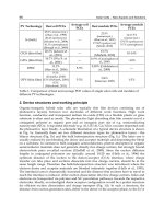
photovoltaics as shown in Table 1.
Major companies Technology Status of manufacturing
Siemens Solar Industries
(SSI), Global Solar
Copper Indium
Diselenide
Initial Small Quantity Manufacture
under 100 kW at SSI
First Solar, BP Solar,
Matsushita
First Solar, BP Solar,
Matsushita
First Solar Production under 1 MW,
Others Lower
Solarex, United Solar, Canon,
others
Amorphous Silicon
Commercial Production under 10 MW
at Several Plants
Table 1. Photovoltaic thin film manufacturing
4.3 Printing of plastic solar cells
Organic semiconductor based solar cells can be integrated fast with textile substrates and
molecular heterojunction cells can be printed using inkjet printing efficiently. This
technology has opened new routes to produce organic solar cells. Credit of invention of
printed solar cells goes to Konarka Technologies
31
for successful demonstration of
manufacturing of solar cells by inkjet printing as shown in Fig.4 .
Fig. 4. Konarka’s plastic photovoltaic cells by printing technology
Solar Cells – New Aspects and Solutions
50
The inkjet printing technology enables manufacturing of solar cells with multiple colors
and patterns for lower power requirement products, like indoor or sensor applications. A
mixture of high and low boiling solvents, (68% orthodichlorobenzene and 32% 1,3,5-
trimethylbenzene), is found suitable for the production of inkjet printed organic solar
cells with power conversion efficiency upto 3%. During the drying process and
subsequent annealing, the suggested oDCB–mesitylene solvent mixture leads to an
optimum phase separation network of the polymer donor and fullerene acceptor and
therefore strongly enhances the performance. During drying and subsequent heat-setting
process, the recommended ortho-dichlorobenzene (oDCB)-mesitylene solvent mixture
leads to an optimum phase separation of polymer donor and fullerene acceptor as
suggested by Pagliaro et al., (2008)
32
. Solvents formulation and temperature of printing
table are two prime parameters to control the spreading and wetting of liquid on
substrate surface. Fig.4 shows a schematic representation of organic film formation by
inkjet printing.
In a typical case, the photoactive formulation is formed by blending poly(3-hexylthiophene)
(P3HT) with fullerene [6,6]-phenyl C61 butyric acid methyl ester (PCBM) in a tetralene and
oDCB–mesitylene solvent mixture. A uniform film and reliable printing with respect to the
spreading and film formation was performed by keeping the inkjet platen temperature 40°C.
The combination of higher/lower boiling solvent mixture, oDCB–mesitylene, offers
following advantages:
a. oDCB with b.p.¼180°C can be used to prevent nozzle clogging and provide a reliable
jetting of the printhead
b. the second component, mesitylene, with lower boiling point of 165°C of the solvent
mixture, with a lower surface tension, is used to achieve optimum wetting and
spreading of the solution on the substrate. It has a higher vapor pressure of 1.86mm Hg
at 20°C and a lower boiling point of 165°C compared to oDCB and tetralene. It increases
the drying rate of the solvent mixture, which is a critical parameter to decide the
morphology of PV prints.
According to Hoth et al., (2007) for an efficient bulk heterojunction solar cell, precise control
of the morphology is essential. The active layer deposition tool strategy decides the
morphology. It was evident from AFM study of the inkjet printed active layers that the
P3HT–PCBM blend films show significant difference in the grain size and surface
roughness. The roughness of active layer surface affects the performance of the inkjet
printed photovoltaic device. The credit of commercialization of power plastic cells (PPC)
goes to Konarka alongwith a German firm Leonhard Kurz by opting simple, energy
efficient, environmentally friendly, replicable and scalable process. The semiconducting
conjugated polymers to make the photosensitive layers of the cell are created in batches of
several liters each. Finally fluffy powder is formed and manufacturers combine it with
standard industrial solvents to create an ink or coatable liquid. This coatable liquid is fed in
reservoir of inkjet print head. Specific types of pumps are used to exert continuous pressure
to maintain constant through put rate from orifice inkjet printhead throughout the printing
process. Inkjet head has facility to move in different directions which helps to create various
printing patterns of semiconducting polymer liquid on textile substrate layer by layer as
shown in Fig.5. These layers are considerably thin. During deposition of semiconducting
polymer cleanliness is very important and whole printing process is carried out in a clean
room
31
.