Ferroelectrics Applications Part 4 pdf
Bạn đang xem bản rút gọn của tài liệu. Xem và tải ngay bản đầy đủ của tài liệu tại đây (5.49 MB, 23 trang )
Ferroelectrics - Applications
58
Dyatlov V.L, Konyashkin V.V., Potapov B.S. & Pyankov Yu.A. (1996). Planar electrostatic
micromotors. Electrical Technology (Elsevier Sequoia), No. 1, pp. 1 – 18, ISSN 1028 –
7957.
Dyatlov V.L., Konyashkin V.V., Potapov B.S. & Pyankov Yu.A. (1991). Film Electrostatics.
Nauka, ISBN 5-02-029683-X, Novosibirsk (in Russian).
Esashi M. & Ono T. (2005). From MEMS to nanomachine. J. Phys. D: Appl. Phys, Vol. 38, No.
13, pp.R223–R230, ISSN 0022-3727.
Harness T. & Syms R. R. A. (2000). Characteristic modes of electrostatic comb-drive X-Y
microactuators. J. Micromech. Microeng., Vol. 10, No. 1, pp. 7–14, ISSN 0960-1317.
Kim B H. & Chun K. (2001). Fabrication of an electrostatic track-following micro actuator
for hard disk drives using SOI wafer. J. Micromech. Microeng., Vol. 11, No. 1, pp.1–6,
ISSN 0960-1317.
Kostsov E.G. & Kamishlov V.F. (2006). Microelectromechanical Micro-Valve. J. nano and
microsys. techn., N 12, pp. 57 -59, ISSN 1813-8586.
Kostsov E.G. & Kolesnikov A.A. (2007). Fast electrostatic microcommutators based on the
ferroelectric films. Ferroelectrics, Vol. 351, No. 1, pp. 138-144, ISSN 0015-0193.
Kostsov E.G. & Malinovsky V.K. (1989). Large-scale use of ferroelectricity in
microelectronics is reality. Ferroelectrics, Vol. 94, No. 4, pp. 457-462, ISSN 0015-0193.
Kostsov E.G. & Sokolov A.A. (2010). Microelectromechanical fuel injector for diesel engines.
Journal of nano and microsystem technique, No 8, pp. 30 – 34, ISSN 1813-8586.
Kostsov E.G. (1995). Ferroelectric films: peculiarities in their application to construction of
new generation of memory devices. Ferroelectrics, Vol. 167, No. 3-4, pp. 169-176,
ISSN 0015-0193.
Kostsov E.G. (2005). Ferroelectric barium-strontium niobate films and multi-layer structures.
Ferroelectrics, Vol. 314, No. 1, pp. 169-187, ISSN 0015-0193.
Kostsov E.G. (2008). Electromechanical energy conversion in the nanometer gaps. Proc. of
SPIE, Vol. 7025, pp. G1-G8, ISSN 0277-786X.
Kostsov E.G. (2009). Status and prospects of micro- and nanoelectromechanics.
Optoelectronics, Instrumentation and Data Processing, Vol. 45, No. 3, pp.189- 226,. ISSN
8756-6990.
Sato K. & Shikida M. (1992). Electrostatic film actuator with a large vertical displacement.
Proceedings of Micro Electro Mechanical Systems, 1992. MEMS’92. An Investigation of
Micro Structures, Sensors, Actuators, Machines and Robot.IEEE, ISBN 0-7803-0497-7,
Travemunde , Germany, 4-7 February, 1992, pp. 1-5,.
Trisnadi J.I., Clinton B.C. & Monteverde R. Overview and applications of Grating Light
Valve
TM
based optical write engines for high-speed digital imaging. (2004). Proc.
SPIE, Vol. 5348, pp. 52-54, ISSN 0277-786X.
Wallrabe U., Bley P., Krevet B., Menz W. & Mohr J. (1994). Design rules and test of
electrostatic micrimotors made by the LIGA process. J. Micromech. Microeng., Vol. 4,
No. 4, pp. 40–45, ISSN 0960-1317.
Yun B. H. (1973). Direct display of electron back tunneling in MNOS memory capacitor.
Appl.Phys.Lett., Vol. 23, No. 3, pp.152-153, ISSN 2158-3226.
Yun B. H. (1974). Measurements of charge propagation in Si
3
N
4
films. Appl. Phys. Lett., Vol.
25, No. 6, pp. 340- 342, 2158-3226.
Zappe S., Baltzer M., Kraus T. & Obermeler E. (1997). Electrostatically driven micro –
actuators: FE analysis and fabrication. J. Micromech. Microeng., Vol. 7, No. 3, pp.204-
209, ISSN 0960-1317.
3
Periodically Poled Acoustic Wave-Guide and
Transducers for Radio-Frequency Applications
Sylvain Ballandras et al.
*
FEMTO-ST, UMR 6174 CNRS-UFC-ENSMM-UTBM, Time&Frequency Dept,
*PHOTLINE Technologies,
France
1. Introduction
The demand for highly coupled high quality acoustic wave devices for RF signal processing
based on passive devices has generated a strong innovative activity, yielding the
investigation of new excitation principles and waveguide structures. Among all the tested
devices, one can mention thick passivation SiO
2
-based structures using high velocity modes
on lithium niobate (LiNbO
3
) or lithium tantalate (LiTaO
3
) (Kando et al, 2006), (Gachon et al.
2010), yielding the definition of interface or isolated-wave-based devices but modes excited
on compound substrates (Elmazria et al, 2009), for instance consisting of a piezoelectric layer
(AlN, ZnO, single crystal LiNbO
3
or LiTaO
3
, etc.) deposited atop a high acoustic wave
velocity material such as diamond-C, silicon carbide, sapphire, silicon, and so on (Higaki et
al, 1997), (Iriarte et al, 2003), (Salut & al, 2010). All these devices generally exploit inter-
digitized transducers (IDTs) operating at Bragg frequency (Morgan, 1985), i.e. exhibiting a
mechanical period equal to a half-wavelength of the acoustic propagation. Although
passivation allows for an improved power handling compared to IDTS on free surfaces, this
feature is still limited by electro-migration and material diffusion phenomena (Greer et al,
1990). An interesting answer to this problem is the use of bulk acoustic waves in thin films
exhibiting a high disruptive field material such as AlN (Lakin, 2003), (Lanz, 2005). In that
case, the frequency control reveals more difficult than for IDT based devices, as the
resonance frequency of the so-called Film Bulk Acoustic Resonators (FBARs) is proportional
to the film thickness. As significant progresses were achieved in thin film technologies
during the last decade, this did not prevent the use of FBARs for actual low-loss RF filter
implementation (Bradley et al, 2000). Nevertheless, it turns out there is still missing
capabilities for better controlling the operation frequency of these passive devices,
particularly for future generations of telecommunication systems which push toward higher
RF bands than those exploited until now.
The idea to transfer the transducer periodicity within the substrate has been shared by
numerous scientists but it took rather a long term before the first experimental evidence,
allowing for a correlation between theory and experiment and hence yielding a satisfying
explanation of the corresponding mode distribution and realistic property description.
*
Emilie Courjon, Florent Bassignot, Gwenn Ulliac, *Jérôme Hauden, Julien Garcia, Thierry Laroche and
William Daniau
Ferroelectrics - Applications
60
Although our very first proof of concept were built on a PZT substrate (Ballandras et al
2003) and after on an epitaxial PZT thin film grown on SrTiO
3
(Sarin Kumar et al, 2004), the
first convincing experiments were performed on 500µm thick 3” LiNbO
3
Z-cut wafers of
optical quality answering severe specifications on total thickness variation and side
parallelism (Courjon et al, 2007). The fabrication of periodically poled transducers (PPTs) on
such wafers has allowed for the excitation of symmetrical Lamb modes with an operating
frequency twice higher than those obtained using standard inter-digitized transducers. The
corresponding devices have been successfully manufactured and tested, the measured
electrical admittances perfectly agreeing with theoretical predictions. As in the case of
classical Lamb waves, the fundamental mode was found almost insensitive to the wafer
thickness. The frequency control then is achieved by the poling period, whereas the
excitation principle coincides with the one of FBARs and hence allows for improved power
handling capabilities regarding standard SAW transducers.
These experiments were followed by the fabrication of PPT-based wave-guides. One more
time, technology advances allowing for room-temperature reliable bonding of
heterogeneous material based on metal-metal compression and lapping/polishing
operations (Gachon et al, 2008), PPTs built on single crystal LiNbO
3
Z-cut layers were
bounded atop Silicon and lapped down to a few tens of µm to develop RF passive devices
compatible with silicon-based technologies (Courjon et al, 2008). Once again, a good
agreement between theory and experiments was emphasized. Two main contributions to
the electrical admittance of the test devices were identified as an elliptical mode and a
longitudinal propagation radiating in the substrate. The first mode was found again low
sensitive to the LiNbO
3
thickness and the technological achievement proved the feasibility
of thinned-LiNbO
3
-layer-based PPT/Silicon devices.
These results were sufficiently convincing for pushing ahead the investigations toward even
more complicated structures. An innovative solution then was proposed to address' the need
for spectral purity, immunity to parasites, simple packaging and fabrication robustness
(Bassignot et al, 2011). The proposed structure is still based on PPT but the later is inserted
between two guiding substrates. It was pointed out first theoretically and afterward
experimentally that a wave could propagate without any acoustic losses and decreases
exponentially in such a structure (definition of a guided mode). This description is close to the
one of interface waves (Kando et al, 2006) and fairly coincides with the behavior of isolated
wave (Elmazria et al, 2009). In the proposed approach however, two metal-metal bonding are
required and naturally provide the excitation electrodes, yielding a significant simplification of
the device fabrication compared to classical IDT-based devices. One more time, theory and
experiments were according well, and the implementation of such a waveguide for the
fabrication of a one-port resonator has been demonstrated (Bassignot et al, 2011). This
resonator was used to stabilize a Colpitts oscillator, allowing for stability measurements.
Another convincing application was demonstrated by Murata (Kadota et al, 2009) for a RF
filter operating at a quite low frequency but exhibiting a double mode transfer function
yielding sharp transition bands, a rejection of about 20 dB with small insertion losses (less than
5 dB). Although not accurately explained in the above-referred text, one can actually guess that
the filter operation is based on mode coupling as the filter architecture does not leave any
possibility for other operation principles.
In this chapter, some fundamental elements are reported to understand the transducer
operation. Theoretical analysis results and theory/experiment assessments are shown,
allowing to illustrate the level of control for designing actual devices based on that principle.
Technological aspects concerning the poling operations as well as bonding and
Periodically Poled Acoustic Wave-Guide and Transducers for Radio-Frequency Applications
61
lapping/polishing techniques are briefly reminded. The fabrication and test of more
complicated waveguides are then described and finally the use of Si/PPT/Si resonators for
oscillator purposes is presented. As a conclusion, further developments needed to widen to
more applications (such as filters or even sensors) are discussed, pointing out the
advantages of the principle but also the points for each more investigations are still needed.
2. Basic principle of PPTs
The Periodically Poled Transducer is fundamentally based on a periodically poled
piezoelectric medium (see Fig.1). Each side of this medium is metalized in order to obtain a
capacitive dipole in which elastic waves can be excited by phase construction. Such a
periodically poled structure can be advantageously achieved on ferroelectric materials like
PZT thanks to the rather small value of its coercive electric field (the absolute value of the
electric field above which the spontaneous polarization can be inverted) or LiNbO
3
and
LiTaO
3
. It advantageously compares to standard surface acoustic wave (SAW) devices
considering its natural operation, yielding a factor of two for the working frequency as it
exploits a second harmonic condition (contrarily to SAW which operates at Bragg frequency).
Also it exhibits an advantage compared to film bulk acoustic resonator (FBAR) as the
periodicity controls the operation frequency (and not only the plate thickness as for FBAR).
As mentioned in introduction, the first mode of most PPT-based device is low sensitive to
the ferroelectrics plate thickness and therefore the solution reveals more robust than bulk
wave devices considering frequency control. An intuitive analysis of the device operation
yields the conclusion that only symmetrical modes can be excited in plates exhibiting
geometrical symmetry. This consideration of course fails as soon as the PPT is bonded on a
substrate, but it still holds for Si/PPT/Si structure.
V
V
Electrodes
p = λ
ac
p
λ
ac
Piezoeloectric substrate
Poled ferroelectrics substrate
(a) (b)
Fig. 1. Comparison between principles of standard SAW devices (a) and poled ferroelectric
film transducers (b)
Whatever, the simulation of PPT cannot be achieved using simple harmonic models or even
Green's function analysis. Even if analytical efforts have been initially achieved to predict
PPT efficiency, the use of finite element analysis has revealed particularly advantageous and
much more flexible than plane-wave expansion approaches for instance (Wilm et al, 2002).
Furthermore, for estimating guiding capabilities of PPT bonded on substrates, the
combination of finite element and boundary element achieved for passivated SAW devices
(Ballandras et al, 2009) or interface waves (Gachon et al, 2010) is ideally suited.
Ferroelectrics - Applications
62
3. Technological developments
3.1 Periodic poling of ferroelectrics single crystal
As mentioned above, the poling process can be rather easily applied to PZT for which the
coercitive field is small enough to allow for an efficient control of the domain polarity. In the
case of lithium niobate or tantalate, this situation is quite different because of the large value
of their coercitive fields (21 MV.m
-1
compared to 2.5 MV.m
-1
max. for PZT). As a
consequence, the development of a dedicated poling bench was required to control the
poling of thick (500µm) Z-cut LiNbO
3
and LiTaO
3
plates. This is detailed in ref (Courjon et
al, 2007). Consequently, only a brief description of the bench principle is reported here. The
poling bench mainly consists of a high voltage amplifier used to submit the ferroelectrics
wafer to an electric field strong enough to invert its native polarization. To achieve such an
operation, one needs the use of optical grade Z-cut plates. Wafers are cut in the same boule
to well control the poling conditions. A photoresist mask is achieved atop one wafer surface,
which defines the poling location. A lithium chloride electrolyte is used to ensure good
electric contacts with the wafer surfaces. A dynamic poling sequence then is imposed to the
wafer, progressively reaching the expected coercitive field. An evidence of successful poling
is obtained by measuring the current of the whole electrical system. Once evidence of
transient current obtained, the device is considered to be poled. Following this sequence,
and providing no short circuit occurs, an almost perfect poling can be achieved. Figure 2
shows a principle scheme of the poling bench.
Fig. 2. Scheme of the poling bench used to fabricate periodically poled ferroelectric plates
Our experiments have been achieved on thick (500 µm) optical quality Z-cut LiNbO
3
plates
from CTI (CA, USA) and on Z-cut LiTaO3 plates from Redoptronics (CA, USA).
Consequently, the voltage needed to invert the domains is approximately 11kV. The
domains to be poled have been defined using a photo-resist pattern on one plate surface
with poling periods (i.e. acoustic wavelengths) ranging from 50 to 5 µm (corresponding to
2.5 and 25 µm line-width respectively). The plate is held in a plexiglas (PMMA) mounting
by means of two O-ring which create two cavities fulfilled by the saturated lithium chloride
solution used as a liquid electrode (as it is shown in the scheme of fig.2).
Periodically Poled Acoustic Wave-Guide and Transducers for Radio-Frequency Applications
63
The high poling voltage is applied to the plate following the sequence established by Myers
et al. (Myers et al, 1995). This sequence is designed to favor the domain nucleation, to
stabilize the inverted domains (i.e. to avoid back-switching of the domains) and to avoid
electrical breakdowns. The poling process is monitored by measuring the electric current
crossing the wafer during the sequence. The signature of a successful domain inversion
corresponds to a voltage dropping, due to the high voltage amplifier saturation, while a
current discharge occurs simultaneously. The poling can be easily controlled by a simple
optical post-observation, as it generates a contrast between at the edge of the poled domains.
We have emphasized that although the LiNbO
3
poling was quicker and simpler than the
LiTaO
3
one, the later was more controllable once increasing the stabilization delay. Figs 3 &
4 show normalized electrical pulse and example of successful poling for both materials.
(a)
(b)
(c)
Fig. 3. (a) Normalized electrical pulse for the LiNbO
3
poling, (b) Electrical potential (green)
and current (red) provided by the amplifier to the poling circuit (c) Optical microscope
observation of a periodically poled lithium niobate substrate
Ferroelectrics - Applications
64
We have tested various configurations of Lamb-wave PPTs, the simplest configuration using
the periodic poling approach just consisting in depositing electrodes on both side of the
poled plate. Both practical implementation and simulations have been developed, based on
the above-described approach and on finite element analysis for the later. Figure 5 shows
that an excellent control of such device and an accurate description of its operation can be
achieved.
(a)
(b)
(c)
Fig. 4. (a) Normalized electrical pulse for the LiTaO
3
poling, (a) Electrical potential (green)
and current (red) provided by the amplifier to the poling circuit (b) Optical microscope
observation of a periodically poled lithium niobate substrate
Periodically Poled Acoustic Wave-Guide and Transducers for Radio-Frequency Applications
65
(a)
(b)
Fig. 5. Theory/experiment assessment for a Lamb wave multi-mode device with 50µm of
poling period built on a Z-cut LiNbO
3
plate (a) and a Z-cut LiTaO
3
plate (b)
3.2 Wafer bonding and lapping/polishing of ferroelectrics upper-layer
The process is based on the bonding of two single-crystal wafers. In this approach, optical
quality polished surfaces are mandatory to favor the wafer bonding. A Chromium and Gold
thin layer deposition is first achieved by sputtering on both ferroelectrics (LiNbO
3
or
LiTaO
3
) and Silicon wafers. Both wafers then are pre-bonded by a mechanical compression
of their metalized surfaces into an EVG wafer bonding machine as shown in Fig.6. During
this process, we heat the material stack at a temperature of 30°C and we apply a pressure of
65N.cm
−2
to the whole contact surface. The bonding can be particularly controlled by
adjusting the process duration and various parameters such as the applied pressure, the
process temperature, the quality of the vacuum during the process, etc. We actually restrict
the process temperature near a value close to the final thermal conditions seen by the device
in operation. Since Silicon and ferroelectrics materials have different thermal expansion
coefficients, one must account for differential thermo-elastic stresses when bonding both
wafers and minimize them as much as possible. A variant to this process has been tested
recently, based on the use of a megasonic cleaning pre-bonder, allowing to significantly
reduce the number of bonding defects. Once the pre-bonding achieved, we finish the
Ferroelectrics - Applications
66
bonding process by applying a strong pressure to the stack which eliminates most of the
bonding defects not due to dusts and organic impurities (the later being eliminated by the
megasonic cleaning), yielding 90% bonded surface and even more.
Fig. 6. Wafer bonding: EVG bonding machine used for wafer pre-bonding (the bonding is
finished using a classical press)
Once the bonding achieved, it is necessary to characterize the adhesion quality. Due to the
thickness of the wafers and the opacity of the stack (metal layers, Silicon), optical
measurements are poorly practicable. As we want to avoid destructive controls of the material
stack, ultrasonic techniques have been particularly considered here. The reliability of the
bonding then is analyzed by ultrasonic transmission in a liquid environment. The bonded
wafers are immersed in a water tank and the whole wafer stack surface is scanned. Fig. 7
presents a photography of the bench. Two focalized transducers are used as acoustic emitter
and receiver. They are manufactured by SONAXIS with a central frequency close to 15 MHz, a
19mm active diameter and a 30mm focal length. The beam diameter at focal distance at -6dB is
about 200µm. Finally Fig.8 shows an example of bonding characterization. One can see that the
bonding is homogeneous and presents few defects. The surface can be considered as bonded
(and specially the area of the PPT one can hardly distinguish).
Fig. 7. Ultrasonic tank for bonding characterization based on acoustic transmission (any
defect in the path of the ultrasonics beam scatters the pressure wave)
Periodically Poled Acoustic Wave-Guide and Transducers for Radio-Frequency Applications
67
Fig. 8. Example of Si/Lithium niobate bonded surface (4-inch wafers), characterized using
ultrasound transmission (Fig. 7)
(a)
(b)
Fig. 9. Photograph of the SOMOS equipment used for lapping/.polishing operations (a) and
SEM view of a lithium niobate wafer bonded on a silicon wafer and finally lapped down to
about 10µm (b)
Ferroelectrics - Applications
68
The piezoelectric wafer is subsequently thinned by a lapping step to an overall thickness of
100 microns. The lapping machine used in that purpose and shown in fig.9 is a SOMOS
double side lapping/polishing machine based on a planetary motion of the wafers (up to 4"
diameter) to promote abrasion homogeneity. We use an abrasive solution of silicon carbide.
We can control the speed of the lapping by choosing the speed of rotation, the load on the
wafer, the rate of flow or the concentration of the abrasive. It is then followed by a micro-
polishing step. This step uses similar equipment dedicated to polishing operation and hence
using abrasive solution with smaller grain. Fig. 9 shows the equipment used to lap and
polish the piezoelectric material and an example of a LiNbO
3
layer thinned down to a few
tenth of microns, bonded on Silicon.
4. PPT/Si wave-guides
Therefore, waveguides based on a thinned LiNbO
3
or LiTaO
3
plate bounded on Silicon have
been implemented along the flow chart of fig.10, taking advantage of the acoustic velocities
in silicon higher than in the above-mentioned materials to meet the guiding conditions.
Here again (as shown in fig.11), the accordance between experimental measurements and
theoretical predictions confirms the control of the device operation and allows for
developing design process.
Fig. 10. Flow chart of the fabrication of PPT/Si waveguide
Fig. 12 presents another comparison between measured responses of the implemented
devices and the theoretical harmonic admittances obtained with our periodic finite element
code. The LiNbO
3
layer thickness has been measured for the devices, allowing for accurate
computations based on realistic parameters. Here are the results for the 40µm period
devices. Since the implemented single-port test devices are quite long and almost behave as
single port resonators, the comparison between measurement and harmonic admittance
results makes sense.
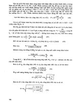
Periodically Poled Acoustic Wave-Guide and Transducers for Radio-Frequency Applications
69
Fig. 11. Theory/experiment comparison for a 20µm period PPT on Silicon (LiNbO
3
thickness =
26µm)
Fig. 12. Theory/experiment assessment for a 40 µm period PPT (LiNbO
3
thickness = 50 µm)
5. Si/PPT/SI-based waveguide, resonator and oscillator
Finally, we have developed an isolated wave guide allowing for the propagation of acoustic
waves within a PPT plate in between two silicon substrates, yielding advanced packaging
opportunities. Fig. 13 illustrates this configuration and Fig.14 shows the kind of theoretical
prediction one can obtained using FEM/BEM harmonic computations to demonstrate the
targeted guiding effect.
Ferroelectrics - Applications
70
V
λ
ac
Electrodes
p = λ
ac
Exponential
vanishing of the
waves
Periodically poled transducer
(PPT)
Silicon
Silicon
Fig. 13. Principle of the PPT isolated wave transducer
Fig. 14. Example of harmonic admittance computed for a Si/LiNbO
3
/Si
transducer/waveguide, the period of the PPT (wavelength) is 50µm, the niobate layer is
30µm thick (the pole is the signature of a guided mode).
The fabrication of acoustic waveguides based on PPTs consists in bonding a silicon wafer on
each side of the periodically poled wafer, as described in fig. 15. In that purpose, the 500 µm
thick Z cut lithium niobate wafer is poled and bonded on a (100) 3" doped silicon wafer
using a wafer bonding technique developed in our group based on a metal-metal adhesion
at room temperature promoted by a high pressure applied to the material stack (Fig.15). The
study of the dispersion properties enables to define a specific configuration using a thinned
PPT layer of about 30 µm. The LiNbO
3
wafer thinning is achieved by home-made lapping
and polishing techniques. After this step, the stack of Si(380 µm)/LiNbO
3
(20 µm) is bonded
again on a doped silicon wafer with the same properties that the first one (Fig.16). Several
devices have been built along this approach but we mainly have focused our attention on
thicker structures (using 500µm thick lithium niobate wafers) for characterization and
application purposes.
Periodically Poled Acoustic Wave-Guide and Transducers for Radio-Frequency Applications
71
Fig. 15. Flowchart which summarizes the different steps of fabrication
Fig. 16. SEM view of a Si/PPT/SI transducer, clearly showing the periodic poling of the
transducer
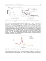
Operational test vehicles have been achieved using doped silicon wafers to ease the
electrical contact. The transducer was built in lithium niobate with a 50 µm period and a
thickness equal to 500 µm. Theoretical and measured electrical admittances agree well and
allow for identifying a main contribution corresponding to a guided longitudinal mode at
131 MHz (fig. 17). The corresponding phase velocity is very close to the one of the PPT alone
(i.e. 6500 m.s
-1
). The elliptically polarized mode excited using the PPT alone and exhibiting a
phase velocity of about 3800 m.s
-1
is not excited nor guided in this configuration. This mode
actually needs a free surface to satisfy its boundary conditions (similarly to a Rayleigh
wave) and therefore, the existence of rigid boundary conditions on each side of the PPT
prevents its excitation and propagation.
This resonator operating near 131 MHz exhibits a quality factor of 13000 and an
electromechanical coupling k
s
2
equal to 0.25 % (twice higher than the one of a SAW resonator
on Quartz). The corresponding phase rotation (320°) and the dynamic of its electrical reflection
coefficient (S
11
=-8 dB) are suitable for oscillator applications. Such a device therefore has been
built using a negative resistance scheme (the so-called Colpitts circuit [Colpitts]).
Ferroelectrics - Applications
72
Fig. 17. Theoretical and experimental admittances of a Si(380µm)/LiNbO
3
(500µm)
PPT/Si(380µm) sandwich
A specific printed circuit has been built in that matter (Fig.18). Note that thanks to the
isolation of the mode, one could glue the resonator directly on the board allowing for easily
grounding the device. A single gold wire then is used to connect the resonator to the
oscillator (such a connection yields a notable sensitivity to RF parasites and hence will be
improved in the next future). The phase noise of the oscillator at 100 kHz from the carrier
shows a value less than -160 dBc/Hz, which can be honestly compared with other acoustic
wave oscillators at such frequency, accounting for the fact that the device was excited with a
quite low signal level (-6dBm). Therefore, increasing the excitation should allow for a
significant reduction of the noise floor and then advantageously compete with standard
solutions. Moreover, as the wave guide appears really robust concerning packaging and
back end conditioning, it can be integrated more easily than any other acoustic wave based
solutions and benefit from a clear applicative potential.
Fig. 18. The oscillator board implemented for phase noise tests
Periodically Poled Acoustic Wave-Guide and Transducers for Radio-Frequency Applications
73
Fig. 19. Phase noise of the 131 MHz oscillator stabilized with a Si/PPt/Si resonator. The
noise floor is better than -160 dBc/Hz.
6. Conclusion
In this chapter, we have discussed the standard techniques implemented for optimizing
PPTs for fabricating test vehicles and we have proposed a detailed analysis of the
experimental tests. We propose some guidelines for future developments and
implementation of these new waveguide principles to answer the requirements for the next
generation of passive signal processing components, and more particularly resonators and
filters. However, because of its very particular configuration, the Si/PPT/Si structure is
considered as a potential candidate for sensor applications, particularly when the sensor is
expected to be inserted in hosting bodies submitted to parametric perturbations such as
stress, vibration or pressure. In that case, the device can be connected directly to the proof
body without the need to protect any surface, providing therefore more robustness than
SAWs or even bulk-wave-based sensors.
7. Acknowledgment
This work has been achieved in the Dominos program framework, funded by the European
Community as the InterReg project DOMINOS and was also funded by the french DGA
(Délégation Générale pour l’Armement) under grant #07-34-020.
8. References
S. Ballandras et al, (2003); A novel surface wave transducer based on periodically poled
piezoelectric domain, Frequency Control Symposium and PDA Exhibition Jointly
with the 17th European Frequency and Time Forum, 2003. Proceedings of the 2003
IEEE International, vol., no., pp. 893- 896
Ferroelectrics - Applications
74
S. Ballandras et al., (2009) A mixed finite element/boundary element approach to simulate
complex guided elastic wave periodic transducers. Journal of Applied Physics 105 1
014911
F. Bassignot et al, (2011) A New Acoustic Resonator Concept Based on Acoustic Waveguides
Using Silicon/Periodically Poled Transducer/Silicon Structures for RF
Applications, IEEE IFCS, San Francisco
P. Bradley et al, (2000), “Film bulk acoustic resonator (FBAR) duplexer” U.S. Patent (USP)
#6262637; Agilent inventors Paul Bradley, John Larson, Richard Ruby).
E. Courjon et al, (2007) Lamb wave transducers built on periodically poled Z-cut LiNbO3
wafers, Journal of Applied Physics, 102, 114107
E. Courjon et al, (2008) Characterization of guided modes excited by periodically poled
transducers on Si," Frequency Control Symposium, 2008 IEEE International , vol.,
no., pp.604-608
O. Elmazria et al, (2009), AlN/ZnO/diamond structure combining isolated and surface
acoustic waves, Applied Physics Letters, vol.95, no.23, pp.233503-233503-3
D. Gachon et al, (2008) Fabrication of High, Frequency Bulk Acoustic Wave Resonator Using
Thinned Single−Crystal Lithium Niobate Layers, Ferroelectrics, Vol.362, n°1, pp.
30−40
D. Gachon et al. (2010) Prediction and Measurement of Boundary Waves at the Interface
Between LiNbO3 and Silicon. IEEE Transactions on Ultrasonics Ferroelectrics and
Frequency Control57 7 1655−1663
J.A. Greer et al, (1990) Metalllisations for Surface Acoustic Wave Resonators: film properties
and device characteristics, Proc. of the IEEE Ultrasonics Symposium, Vol.1, pp.483-
491
G.F. Iriarte et al, (2003) SAW COM parameter extraction in AlN/diamond layered
structures, IEEE Trans. on UFFC, Vol. 50, N°11, pp. 1142–1547
K. Higaki et al, (1997) High power durability of diamond surface acoustic wave filter,
Ultrasonics, Ferroelectrics and Frequency Control, IEEE Transactions on , vol.44,
no.6, pp.1395-1400
M. Kadota et al, (2009) Acoustic Wave Devices using Periodical Poled Z-cut LiTaO
3
Plate,
Proc. of the joint IEEE IFCS-EFTF, Besançon, pp919-922, 2009
H. Kando et al (2006) 6B-4 RF Filter using Boundary Acoustic Wave, Ultrasonics
Symposium, IEEE, vol., no., pp.188-191
R. Lanz, P. Muralt, (2005) Band pass filters for 8 GHz using solidly mounted Bulk Acoustic
Wave Resonators, IEEE Trans. on UFFC, Vol. 52, N°6, pp. 946–946
K.M. Lakin, (2003) “Thin film resonator technology”, Proc. of the joint IEEE IFCS-EFTF, pp.
1-14
D.P. Morgan, (1985) Surface Wave Devices for Signal processing, Studies in Electrical Eng.
19, Elsevier Ed.
L. E. Myers et al, (1995) Quasi-phase-matched optical parametric oscillator”, JOSA B, Vol. 12,
Issue 11, pp. 2102-2116
R. Salut & al, (2010) Fabrication of GHz Range Oscillators Stabilized by Nano-Carbon-
Diamond-Based Surfcae Acoustic Resonators, Proc of the IEEE International
Ultrasonics Symposium, San Diego
A. K. Sarin Kumar et al (2004), High-frequency surface acoustic wave device based on thin-
film piezoelectric interdigital transducers, Appl. Phys. Lett. 85, 1757
doi:10.1063/1.1787897 (3 pages)
M. Wilm et al, (2002) A full 3D plane-wave-expansion model of 1-3 piezoelectric composite
structures, J. Acoust. Soc. Am., vol. 112, n°3, pp. 943-952
4
Ferroelectric Polymer for Bio-Sonar Replica
Antonino S. Fiorillo and Salvatore A. Pullano
School of Biomedical Engineering, University of Magna Græcia,
Italy
1. Introduction
The sensorial knowledge paradigm has captured the interest of many eminent scholars in past
centuries (the philosophical trend of “Sensism” was developed around the “Gnoseologic
Paradigm”, which has found its highest expression in Étienne Bonnot de Condillac, 1930) as
well as in the modern era, particularly in the attempt to interface the external environment to
humans through artificial systems. Of the five human senses, which have been investigated by
scientists involved in artificial perception studies, vision, touch and hearing have received the
most attention, each one for different reasons. When referring to hearing as the sense which
perceives sound (the mechanical perturbation induced in a medium by a travelling wave at
suitable frequency), a distinction should be made. Indeed, sound between 100 Hz and 18 kHz
refers mainly to the range of human perception, while infrasound (up to 20 or 30 Hz) and low
frequency ultrasound (from 20 to 120 kHz) refer to animal (mammalian) perception.
Low frequency ultrasounds have been amply investigated in the last century and the
resulting applications have been made in both military and civil fields. In any case, it
appears relevant and necessary to improve the performance of the ultrasonic system (more
properly named sonar) for use in a variety of industrial, robotic, and medical applications
where ranging plays a basilar role. Nevertheless, other important information can be
extrapolated through proper use of the ultrasonic signal as is evident from the study of the
biology and mammalian behaviour (Altringham, 1996). Up to now, attempts have been
made to try to emulate animal auditory systems by using both commercial or custom
piezoelectric transducers. In this context, the latest investigation in artificial perception was
mainly inspired by bat bio-sonar, which has been extensively studied and described by
biologists.
As a result of the damping exerted by the propagation medium, which increases as the
ultrasound frequency increases, conventional transducers normally function at relatively
low frequencies (40 ÷ 50 kHz) in air. Sometimes this restricts choices of piezoelectric
materials, besides transducer shape and dimensions. In order to increase the frequency and
hence to improve the performances of ultrasonic transducers, flexible plastic materials, such
as the ferroelectric polymer polyvinylidene fluoride (PVDF) were investigated and
assembled in different geometries. It was discovered that, when properly shaped, PVDF
films can resonate at frequencies superior to 100 kHz, covering the full range frequency of
the majority of bat bio-sonars (20 ÷ 120 kHz).
The first part of a work aimed at emulating the auditory system of Pteronotus Parnellii, (also
known as the moustached bat) is described in this chapter. We have simulated some of this
Ferroelectrics - Applications
76
bat’s most important strategies, based on the techniques used by its sophisticated echo-
location system in gathering ultrasonic information. Specifically, in this phase of the study,
the piezoelectric transducer is used to emulate the function of the bat cochlea in a real
distance measurement, although bio-sonar capabilities are far superior.
The chapter is organized as follows: first the design and characterization of the ferroelectric
polymer ultrasonic transducer is discussed. Based on the piezoelectric equilibrium rules, a
suitable transducer geometry has been designed in order to improve the device’s
performance in air.
Then the transducer impedance has been characterized from 30 to 40 kHz up to 120 kHz,
exactly in the same range frequency in which most bat bio-sonars operate. The design of the
electronic circuits and the matching of the electric impedance with the ultrasonic transducer
received particular attention because of the inherent noise of the PVDF. The sensory unit
operates at distances of 10 ÷ 2500 mm with an axial resolution of about 2 mm down to 500
µm. A critical comparison between the custom transducer (based on ferroelectric polymer
technology) and similar devices (based on different, but standard, technologies) is also
carried out.
These and other problems are considered in this work, including a neural network approach
carried out in order to verify the potentiality of the PVDF electronic sonar and the
analogism with the bat bio-sonar, in all its complexity, with the aim of exploring how
artificial perception in the acoustic field can support human sensorial perception.
Nomenclature
c Stiffness coefficient [
2
Nm
−
⋅ ]
d Piezoelectric constant [
1
CN
−
⋅ ]
C Capacitance [
F ]
D
Normal electric displacement [
2
Cm
−
⋅ ]
e Piezoelectric constant [
2
Cm
−
⋅ ]
E Electric field [
1
Vm
−
⋅ ]
f
Frequency [Hz ]
g
Piezoelectric constant [
1
VmN
−
⋅⋅ ]
h Piezoelectric constant [
1
Vm
−
⋅ ]
I
Electric current [
A
]
k Piezoelectric coupling factor
L Inductance [ H ]
M
Figure of merit
P Polarization [
2
Cm
−
⋅ ]
Q Quality factor
R
Resistance [
Ω
]
r Bending radius [ m ]
S Strain
s Elastic compliance [
21
mN
−
⋅ ]
T Tangential stress [
2
Nm
−
⋅ ]
β
Dielectric impermeabilities [
1
mF
−
⋅ ]
ε
Permittivity [
1
Fm
−
⋅ ]
r
ε
Relative permittivity
0
ε
Vacuum permittivity [
1
Fm
−
⋅ ]
Ferroelectric Polymer for Bio-Sonar Replica
77
ϕ
Angle [de
g
]
SNR Signal-to-noise ratio
2. PVDF transducer analogy to bat cochleas
The auditory system of mammals is characterized by a common basic layout in which one
can identify three anatomical regions—the external and middle ears (air filled) and the inner
ear (filled with biological fluid). The acoustic waves are received, conveyed, and amplified
by the external and middle ears, while the vibrational energy related to sound pressure is
converted into bio-electric energy by the inner ear. Sound amplification is carried out
mechanically by a system which includes the ossicles: the malleus, the incus, and the stapes;
and the eardrum.
In the system we propose for bio-sonar replication, the amplification of the signal and all
other steps included in acoustical signal conditioning are carried out electronically, while
the piezoelectric transducer is concerned with the conversion of mechanical energy. Our
attention was focalized on the third anatomic region, particularly the cochlea, which
transduces mechanical energy into bio-electrical energy, and the acoustic nerve, which
carries the bio-electrical signal to the cerebral cortex.
In this section the anatomic structure of the cochlea and its working is reviewed in order to
clarify and justify the choice concerning materials, particularly the ferroelectric polymer,
and methods used to emulate the bio-sonar of bats.
The cochlea of a bat, similar to that of other mammals, boasts a hollow spiral geometry
divided into three channels; the vestibular and tympanic channels are filled with
endolymph, which is very similar to intracellular liquid, and the middle channel is filled
with perilymph, similar to extracellular liquid, each one separated by an endothelial
membrane (see Figure 1). As far as the electronic system is concerned, the most important
component is the basilar membrane which, through vibration, activates the receptors of the
organ of Corti, that lie over it (the organ of Corti includes the tectorial membrane, two
different systems of hair cells, and nervous fibres; these generate bio-pulses as a
consequence of the vibration).
Fig. 1. Main part of the inner ear and arrangement of cochlear component.
Ferroelectrics - Applications
78
When the acoustic wave reaches the eardrum after passing through the outer ear canal, it
has already been primarily amplified in this resonant cavity of the external ear.
Successively it is mechanically amplified in the middle ear by the chain of ossicles acting
as levers on the oval window, located in the inner ear. The travelling wave, once in the
cochlea, propagates along the basilar membrane (see Figure 2), which acts as a mechanical
filter with respect to the frequency spectrum. Different frequency components of the
signal cause the motion of different parts of the membrane in a tonotopic organization.
The behaviour of the basilar membrane is related to its geometry, because moving from
the base toward the apex the membrane increases its width and thickness, while the
resonance frequency decreases.
Fig. 2. Basilar membrane winding inside the cochlea
The receptors located in the organ of Corti are divided into outer and inner hair cells, and
perform two different functions. The motion of the basilar membrane intimately connected
to the organ of Corti is first amplified by the outer hair cells and then transmitted through
the liquid to the tectorial membrane that induces the deflection of the hair in the inner cells.
The inner hair cells transduce the mechanical signal, after amplification, into an
electrochemical signal through the activation of ionic channels and the release of a
neurotransmitter (glutamate) to the acoustic nerve, as a consequence of the polarization
level of the cells itself. The neurotransmitter reaches the central nervous system through the
afferent fibres, which account for 90 ÷ 95 % of the total connections, while the rest are
connected to the inner hair cells. From the bio-electrical point of view, this process is
concerned with the generation of an action potential which drives ionic currents along the
axons of the afferent fibres (see Figure 3); conversely, the majority of the efferent fibres connect
the central nervous system to the outer hair cells.
Referring to the analogism with the artificial system, the PVDF ultrasonic transducer acts in
a way similar to the basilar membrane, except for the absence of the outer hair cells. In effect
though, the acoustic pressure is not mechanically amplified, but merely converted, by the
direct piezoelectric effect , into an electrical signal and, hence, only
afferent electronic pathways
are considered.
PVDF is a light and flexible plastic material, of several tens of μm in
thickness, which can be shaped into hemicylindrical geometries in order to fabricate the
ultrasonic transducer which resonates in the frequency range of bat biosonar.
The resonance
frequency is inversely proportional to the bending radius and can be easily tuned to the
suitable values necessary for the specific tasks accomplished by the bat. In fact the curved
PVDF ultrasonic transducer works in a way similar to the basilar membrane.
Ferroelectric Polymer for Bio-Sonar Replica
79
Fig. 3. Structure of hair cell and axon with generated potential along it. The synapses carries
the neurotransmitter molecules through the axon. The nodes of Ranvier refresh action
potential through the pathway.
The electric dipoles in piezo-polymer, upon the application of an external pressure, generate
a net electric charge (which is conveyed through the
afferent electronic pathways to the central
processing system); the inner hair cells also generate a bio-electrical stimulus upon
deflection of the basilar membrane. In the next section of this chapter we briefly introduce
the ferroelectric phenomenon in PVDF with emphasis on the piezoelectric effect and we
describe the design and characterization of the ultrasonic transducer.
3. Polyvinylidene fluoride (PVDF) polymer
To understand the behaviour of ferroelectric materials and their field of application as
sensors, we look at both the piezoelectric and pyroelectric effects. Crystals without centers
of symmetry may have one or more polar axes and show both vectorial and tensorial
properties. Since they exhibit spontaneous polarization, they are defined polar crystals,
which display a pyroelectric effect, that is, a change in polarization under a gradient of
temperature (Jona & Shirane, 1962; Berlincourt, 1981). In addition, polar crystals exhibit both
a direct piezoelectric effect (a state of electrification caused by a mechanical deformation)
and a converse piezoelectric effect (a mechanical deformation caused by the exertion of an
external electric field) (Curie, 1880). At the end of the 60’s, the discovery of strong
piezoelectric (Kawai, 1969) and pyroelectric activity (Bergman et al., 1971) in PVDF ascribed
the polymer to the family of synthetic ferroelectric polycrystals.
3.1 Atomic structure and morphology
Polyvinylidene fluoride is a semicrystalline linear polymer, with long molecular chains in
which each monomer
22
CH CF−−−
⎡
⎤
⎣
⎦
has a dipole moment. It is synthesized in poly-
crystalline forms, the most important of which are the α and β forms shown in Figure 4. In
the α form (or form II), obtained by fusion, the lattice has a monoclinic unit cell with 2/m
symmetry and contains trans-gauche/trans-gauche molecular conformation (TGTG’). The β
form (or form I) is obtained from the
α form by low temperature stretching. In this case, the
lattice unit cell is orthorhombic with mm2 symmetry and all-trans zigzag molecular
Ferroelectrics - Applications
80
conformation (TTTT). Unlike the α antipolar crystal form, the β form is piezoelectric and
exhibits spontaneous polarization. Although there are two other crystalline structures α
p
and γ, for technological purposes the β form is the most interesting due to its stronger
piezoelectric and pyroelectric properties (Davis, 1988).
Fig. 4. Representation of crystalline α (upper) and β (lower) forms. Arrows indicate the
orientation of the dipole moment.
3.2 Poling methods
Because of its molecular conformation, unoriented PVDF in the α form does not exhibit large
piezoelectric and pyroelectric coefficients. In order to induce reproducible ferroelectric
characteristics, the polymer must be oriented and poled (a higher degree of orientation results
in increased piezoelectric activity). There are several techniques for poling PVDF including:
corona poling, thermal poling, plasma and higher electric field poling, and simultaneous
poling/stretching techniques. Starting with a non-polar α form, the polymer film is heated to
50 ÷ 60 °C and then uniaxially stretched along direction 1 called the “Machine Direction” or
alternatively stretched biaxially along direction 2, called the “Transverse Direction”, as shown
in Figure 5. Stretching recrystallizes the PVDF in the β form, which renders it suitable to be
poled using some of the previously mentioned techniques.
Fig. 5. Fundamental directions of PVDF film