Heat Transfer Engineering Applications Part 4 potx
Bạn đang xem bản rút gọn của tài liệu. Xem và tải ngay bản đầy đủ của tài liệu tại đây (1.44 MB, 30 trang )
Energy Transfer in Ion– and Laser–Solid Interactions 9
0 1000 2000 3000 4000
500
1000
1500
Temperature [K]
Depth [nm]
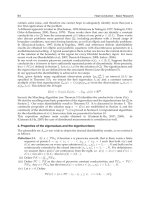
140 ns
(a) Temperature profile. (b) Extinction spectra.
Fig. 6. Effects of excimer laser on silver nano–particles embedded in SiO
2
: (a) Temperature
profile as function of depth, 70 ns after the maximum irradiance of a 2.8 J/cm
2
pulse. (b)
Extinction spectra of samples treated with increasing laser fluences.
By means of a 6 ns FWHM pulsed Nd:YAG laser at 1064 nm and at 532 nm (Crespo-Sosa &
Schaaf (n.d.)), samples containing Ag and Au nano–particles, prepared with the same method
described above, were also irradiated. At this wavelength, energy is absorbed mainly by the
matrix and little or no reduction is observed in the nano–particles size as they do not melt.
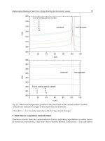
On the contrary, in Fig. 7, one can see, that the first 10 pulses remove the surface carbon
deposited (few nanometers below the surface) during Ag and Au implantation, and therefore
the “background” drops. After 100 pulses, the resonance has turned narrower, indicating a
slight growth of the nano–particles, but this growth does not continue after 1000 or 10000
pulses. In this case, the calculation of the temperature evolution indicates no significant
increment. This means that this slight growth is not produced by a thermal process, and
that another mechanism must be present.
0
0.5
1
1.5
2
200 325 450 575 700
Pristine
10 Pulses
100 pulses
1 000 pulses
10 000 pulses
Wavelength [nm]
O. D. [a.u.]
Fig. 7. Effects of infrared laser on Ag nano–particless embedded in SiO
2
: Extinction spectra
of samples treated with increasing number of pulses.
When irradiating these samples with a wavelength of 532 nm, we observed opposite effects
between silver and gold nano–particles. This is because the resonance of gold nano–particles
79
Energy Transfer in Ion– and Laser–Solid Interactions
10 Will-be-set-by-IN-TECH
falls very close to the irradiation wavelength, while the resonance for silver is around 400 nm.
In other words, the system with Ag nano–particles absorbs the energy uniformly by the
matrix, whereas Au nano–particles absorb the energy in the other case. By tunning the
wavelength, one can select whether to provoke effects directly on the nano–particles or onto
the matrix.
Nano–particles decomposition and accompanying surface ablation is usually related to the
energy absorbed, the location and the duration of the pulse. The shorter the pulse is,
the higher the temperature that the nano–particles can reach and therefore the lower the
ablation threshold. This has been experimentally verified with nanosecond pulses, but with
picosecond pulses, non thermal effects may appear. For example, when Ag nano–particles
are irradiated with 26 ps pulses at 355 nm , a surprisingly high ablation threshold is found
(Torres-Torres et al. (2010)). The cause for this, is not fully understood. The measured
non-linear absorption coefficient is, from the thermal point of view, negligible to account
for such an effect. On the other hand, it has been reported that two–photon absorption, (an
equally improbable event) can be important in the determination of the melting threshold of
silicon by ps laser pulses at 1064 nm (van Driel (1987)).
From a merely thermal point of view, the use of shorter laser pulses can be treated ”locally”
as the heat diffusion length becomes shorter. Xia and co–workers have, for example, modeled
the temperature evolution of a nano–particle embedded in a transparent matrix by means of
Eq. 2. And from this calculation , they showed that the corresponding thermal stress and phase
transformations are important in the description of surface ablation and of nano–particles
fragmentation (Xia et al. (2006)). Picosecond and femtosecond pulses can provoke damage in
materials that can also be treated thermally. It has been mentioned above, that typically, hot
electrons transfer their energy to the lattice in times shorter than few picoseconds. When
pulses shorter than this time are used, the dynamics of the electrons must be taken into
account. Today’s main interest in such pulses is precisely the possibility of studying the
dynamic evolution of the system. In this case, Eq. 2 is used to test if the fundamental
parameters of the electron-electron and electron-phonon interactions are properly reproduced
by the proposed model (Bertussi et al. (2005); Bruzzone & Malvaldi (2009); Dachraoui &
Husinsky (2006); Muto et al. (2008); Zhang & Chen (2008)). It is in a certain way the inverse
problem where the thermal properties are to be determined. Another fine example, where
the calculation of the electronic temperature by means of Eq. 2 plays an important role,
is the determination of the contribution of the hot electrons to the third–order non–linear
susceptibility of gold nano–particles (Guillet et al. (2009)).
5. Discussion
As seen above, the methodology for studying the temperature increase in the material due to
laser– or to ion–irradiation has been well established using the heat equation. However, let us
make a few remarks on it:
Even though calculations are not too sensitive to changes in the values of the thermal
properties, the uncertainty of them should always be a concern. The processes involved occur
and also cause high pressure regions, where a state equation of the system can hardly be
known. Additionally, the possibility of a change in these values in nano–structures must also
be considered (Buffat & Borel (1976)). Also, the possibility of non–Fourier’s heat conduction
has not been discussed enough (Cao & Guo (2007); Rashidi-Huyeh et al. (2008)). Indeed, it
is not always clear how important a variation in such parameters is or how important the
consideration of a particular effect is.
80
Heat Transfer - Engineering Applications
Energy Transfer in Ion– and Laser–Solid Interactions 11
Another problem to be considered, is the cumulative nature of the effects. Most of the
calculations are based on single events, an ion or a pulse, and then scaled, while events might
be cumulative. Neither are charge effects considered in these kinds of calculation and they
might, in some cases, have an important influence on the effects observed. Also, most of the
calculations have been simplified to solve the one dimensional heat equation (Awazu et al.
(2008)).
The process in which the ion deposits its energy to the nuclei of the target is highly stochastic.
The ion does not follow a straight line and the energy deposition density (F
d
) is not uniform.
The process described by the heat equation, must be then considered as an “average” event, as
in an statistical point of view. Furthermore, the description through the heat equation assumes
thermal equilibrium and energy transfer, but during the first stages of the process, the energy
is limited to only few atoms, that move with high kinetic energy, that might be better described
by a ballistic approach. Indeed, there are effects (in ion beam mixing, for instance), that are
directly related to the primary knock-on collisions, that cannot be described by the thermal
equation.
The interaction of the ion with the electrons can be thought as more uniform because the
electron density is much higher, but additional parameters arise, like the coupling function
g in Eq. 2 and the thermal properties of the electronic cloud. In this case, the consideration
of the “ballistic” range of the ejected electrons by the ion is important to input correctly the
spatial deposition of energy.
Though in principle simpler, the interaction of high power lasers with matter also present
interesting challenges to consider, first, the effects that raise due to high intensity pulses,
in which the absorption and conductive processes might be altered within the same pulse,
and the effects due to the ultrashort pulses that might be even faster than the system
thermalization.
6. Conclusions
In this chapter, it has been reviewed how the simple, yet powerful concepts of classical heat
conduction theory have been extended to phenomena like ion beam and laser effects on
materials. These phenomena are characterized by the wide range of temperatures involved,
extreme short times and high annealing and cooling rates, as well as by the nanometric
spaces in which they occur. In consequence, there is a high uncertainty in the values of the
thermal properties that must be used for the calculations. Nevertheless, the calculations done
up-today have proved to be very useful to describe the effects of them. They also agree with
other methods like Monte Carlo and molecular dynamics simulations. In the future these
parameters must be better determined (theoretically and experimentally) and further applied
to more complex systems, like nano–structured materials as well as to femto and atosecond
processes. The knowledge of the fundamentals of radiation interaction behind these processes
will benefit a lot from thess new experimental, theoretical and computational tools.
7. Aknowledgments
The author would like to thank all the colleagues, technicians and students that have
participated in the experiments described above. And to the following funding organizations:
CONACyT, DGAPA-UNAM, ICyTDF and DAAD.
81
Energy Transfer in Ion– and Laser–Solid Interactions
12 Will-be-set-by-IN-TECH
8. References
Awazu, K., Wang, X., Fujimaki, M., Tominaga, J., Aiba, H., Ohki, Y. & Komatsubara, T. (2008).
Elongation of gold nanoparticles in silica glass by irradiation with swift heavy ions,
Physical Review B 78(5): 1–8.
URL: />Bertussi, B., Natoli, J., Commandre, M., Rullier, J., Bonneau, F., Combis, P. & Bouchut, P.
(2005). Photothermal investigation of the laser-induced modification of a single gold
nano-particle in a silica film, Optics Communications 254(4-6): 299–309.
URL: />Bruzzone, S. & Malvaldi, M. (2009). Local Field Effects on Laser-Induced Heating of Metal
Nanoparticles, The Journal of Physical Chemistry C 113(36): 15805–15810.
URL: />Buffat, P. & Borel, J. (1976). Size effect on melting temperature of gold particles, Physical Review
A 13(6): 2287.
URL: />Cao, B Y. & Guo, Z Y. (2007). Equation of motion of a phonon gas and non-Fourier heat
conduction, Journal of Applied Physics 102(5): 053503.
URL: />Cheang-Wong, J. C., Oliver, A., Crespo-Sosa, A., Hernández, J. M., Muñoz, E. &
Espejel-Morales, R. (2000). Dependence of the optical properties on the ion implanted
depth profiles in fused quartz after a sequential implantation with Si and Au ions,
Nuclear Instruments and Methods in Physics Research Section B: Beam Interactions with
Materials and Atoms 161-163: 1058–1063.
URL: />Chettah, a., Kucal, H., Wang, Z., Kac, M., Meftah, a. & Toulemonde, M. (2009). Behavior
of crystalline silicon under huge electronic excitations: A transient thermal spike
description, Nuclear Instruments and Methods in Physics Research Section B: Beam
Interactions with Materials and Atoms 267(16): 2719–2724.
URL: />Crespo-Sosa, A. & Schaaf, P. (n.d.). Unpublished.
Crespo-Sosa, A., Schaaf, P., Reyes-Esqueda, J. A., Seman-Harutinian, J. A. & Oliver, A. (2007).
Excimer laser absorption by metallic nano-particles embedded in silica, Journal of
Physics D: Applied Physics 40(7): 1890–1895.
URL: />84bf900042
Dachraoui, H. & Husinsky, W. (2006). Fast electronic and thermal processes in femtosecond
laser ablation of Au, Applied Physics Letters 89(10): 104102.
URL: />Daraszewicz, S. & Duffy, D. (2010). Extending the inelastic thermal spike model for
semiconductors and insulators, Nuclear Instruments and Methods in Physics Research
Section B: Beam Interactions with Materials and Atoms 269(14): 1646–1649.
URL: />D’Orléans, C., Stoquert, J., Estournès, C., Cerruti, C., Grob, J., Guille, J., Haas, F., Muller, D. &
Richard-Plouet, M. (2003). Anisotropy of Co nanoparticles induced by swift heavy
ions, Physical Review B 67(22): 10–13.
URL: />82
Heat Transfer - Engineering Applications
Energy Transfer in Ion– and Laser–Solid Interactions 13
D’Orléans, C., Stoquert, J., Estournes, C., Grob, J., Muller, D., Cerruti, C. & Haas, F. (2004).
Deformation yield of Co nanoparticles in SiO
2
irradiated with 200 MeV
127
I ions,
Nuclear Instruments and Methods in Physics Research Section B: Beam Interactions with
Materials and Atoms 225(1-2): 154–159.
URL: />D’Orléans, C., Stoquert, J., Estournes, C., Grob, J., Muller, D., Guille, J., Richardplouet, M.,
Cerruti, C. & Haas, F. (2004). Elongated Co nanoparticles induced by swift heavy
ion irradiations, Nuclear Instruments and Methods in Physics Research Section B: Beam
Interactions with Materials and Atoms 216(1-2): 372–378.
URL: />Duffy, D. M., Itoh, N., Rutherford, a. M. & Stoneham, a. M. (2008). Making tracks in metals,
Journal of Physics: Condensed Matter 20(8): 082201.
URL: />fd4082dde60
Duffy, D. M. & Rutherford, a. M. (2007). Including the effects of electronic stopping
and electron-ion interactions in radiation damage simulations, Journal of Physics:
Condensed Matter 19(1): 016207.
URL: />b1a3956294e00
Elsayed-Ali, H., Norris, T., Pessot, M. & Mourou, G. (1987). Time-Resolved Observation of
Electron-Phonon Relaxation in Copper, Physical Review Letters 58(12): 1212–1215.
URL: />Giulian, R., Kluth, P., Araujo, L., Sprouster, D., Byrne, A., Cookson, D. & Ridgway, M. (2008).
Shape transformation of Pt nanoparticles induced by swift heavy-ion irradiation,
Physical Review B 78(12): 1–8.
URL: />Johannessen, B., Kluth, P., Giulian, R., Araujo, L., Leewelin, D.J., Foran, G.J., Cookson, D. &
Ridgway, M. (2008). Modification of embedded Cu Nano–particles: Ion irradiation
at room temperature., Nuclear Instruments and Methods in Physics Research Section B:
Beam Interactions with Materials and Atoms 257(1-2): 37–41.
URL:
Guillet, Y., Rashidi–Huyeh, M. & Palpant. B. (2009). Influence of laser Pulse characteristics
on the hot electron contribution to the third–order nonlinear optical response of gold
nanoparticles., Physical Review B 79: 045410.
URL:
Katz, R. & Varma, M. N. (1991). Radial distribution of dose., Basic life sciences 58: 163–79;
discussion 179–80.
URL: />Klaumunzer, S. (2006). Modification of nanostructures by high-energy ion beams, Nuclear
Instruments and Methods in Physics Research Section B: Beam Interactions with Materials
and Atoms 244(1): 1–7.
URL: />Kluth, P., Giulian, R., Sprouster, D. J., Schnohr, C. S., Byrne, a. P., Cookson, D. J. &
Ridgway, M. C. (2009). Energy dependent saturation width of swift heavy ion shaped
embedded Au nanoparticles, Applied Physics Letters 94(11): 113107.
URL: />83
Energy Transfer in Ion– and Laser–Solid Interactions
14 Will-be-set-by-IN-TECH
Kluth, P., Johannessen, B., Giulian, R., Schnohr, C. S., Foran, G. J., Cookson, D. J., Byrne, A. P.
& Ridgway, M. C. (2007). Ion irradiation effects on metallic nanocrystals, Radiation
Effects and Defects in Solids 162(7): 501–513.
URL: />221&magic=crossref||D404A21C5BB053405B1A640AFFD44AE3
Lin, Z. & Zhigilei, L. (2007). Temperature dependences of the electron-phonon coupling,
electron heat capacity and thermal conductivity in Ni under femtosecond laser
irradiation, Applied Surface Science 253(15): 6295–6300.
URL: />Meldrum, A., Boatner, L. & White, C. (2001). Nanocomposites formed by ion implantation:
Recent developments and future opportunities, Nuclear Instruments and Methods in
Physics Research Section B: Beam Interactions with Materials and Atoms 178(1-4): 7–16.
URL: />Mota-Santiago, P. E., Crespo-Sosa, A., Jiméenez-Hernáandez, J. L., Silva-Pereyra, H G.,
Reyes-Esqueda, J. A. & Oliver, A. (2011). Noble-Metal Nano-Crystal Aggregation
in Sapphire by Ion Irradiation And Subsequent Thermal Annealing, Journal of Physics
D: Applied Physics submitted.
Mota-Santiago, P. E., Crespo-Sosa, A., Jiméenez-Hernáandez, J. L., Silva-Pereyra, H G.,
Reyes-Esqueda, J. A. & Oliver, A. (2012). Ion beam induced deformation of gold
nano-particles embedded in Sapphire.
Muto, H., Miyajima, K. & Mafune, F. (2008). Mechanism of Laser-Induced Size Reduction of
Gold Nanoparticles As Studied by Single and Double Laser Pulse Excitation, Journal
of Physical Chemistry C 112(15): 5810–5815.
URL: />Oliver, A., Reyes-Esqueda, J. A., Cheang-Wong, J. C., Román-Velázquez, C., Crespo-Sosa, A.,
Rodríguez-Fernández, L., Seman-Harutinian, J. A. & Noguez, C. (2006). Controlled
anisotropic deformation of Ag nanoparticles by Si ion irradiation, Physical Review B
74(24): 1–6.
URL: />Penninkhof, J. J., Polman, A., Sweatlock, L. a., Maier, S. a., Atwater, H. a., Vredenberg, a. M.
& Kooi, B. J. (2003). Mega-electron-volt ion beam induced anisotropic plasmon
resonance of silver nanocrystals in glass, Applied Physics Letters 83(20): 4137.
URL: />Penninkhof, J. J., van Dillen, T., Roorda, S., Graf, C., Vanblaaderen, A., Vredenberg, a. M. &
Polman, A. (2006). Anisotropic deformation of metallo-dielectric core-shell colloids
under MeV ion irradiation, Nuclear Instruments and Methods in Physics Research Section
B: Beam Interactions with Materials and Atoms 242(1-2): 523–529.
URL: />Rangel-Rojo, R., Reyes-Esqueda, J. A., Torres-Torres, C., Oliver, A., Rodríguez-Fernández, L.,
Crespo-Sosa, A., Cheang-Wong, J. C., McCarthy, J., Bookey, H. & Kar, A. (2010).
Linear and nonlinear optical properties of aligned elongated silver nanoparticles
embedded in silica, in D. Pozo Perez (ed.), Silver Nanoparticles, InTech, pp. 35 – 62.
URL: />-of-aligned-elongated-silver-nanoparticles-embedded-in-silica
Rashidi-Huyeh, M., Volz, S. & Palpant, B. (2008). Non-Fourier heat transport in
metal-dielectric core-shell nanoparticles under ultrafast laser pulse excitation,
84
Heat Transfer - Engineering Applications
Energy Transfer in Ion– and Laser–Solid Interactions 15
Physical Review B 78(12): 1–8.
URL: />Ridgway, M., Giulian, R., Sprouster, D., Kluth, P., Araujo, L., Llewellyn, D., Byrne, a.,
Kremer, F., Fichtner, P., Rizza, G., Amekura, H. & Toulemonde, M. (2011). Role of
Thermodynamics in the Shape Transformation of Embedded Metal Nanoparticles
Induced by Swift Heavy-Ion Irradiation, Physical Review Letters 106(9): 1–4.
URL: />Rodríguez-Iglesias, V., Peña Rodríguez, O., Silva-Pereyra, H G., Rodríguez-Fernández, L.,
Cheang-Wong, J. C., Crespo-Sosa, A., Reyes-Esqueda, J. A. & Oliver, A. (2010).
Tuning the aspect ratio of silver nanospheroids embedded in silica., Optics letters
35(5): 703–5.
URL: />Ryazanov, A., Volkov, A. & Klaumünzer, S. (1995). Model of track formation, Physical Review
B 51(18): 12107–12115.
URL: />Sands, D. (2011). Pulsed laser heating and melting, in Vyacheslav S. Vikhrenko (ed.), Heat
Conduction / Book 2, InTech, pp. .
URL: />Schmidt, B., Heinig, K H., Mücklich, A. & Akhmadaliev, C. (2009). Swift-heavy-ion-induced
shaping of spherical Ge nanoparticles into disks and rods, Nuclear Instruments and
Methods in Physics Research Section B: Beam Interactions with Materials and Atoms
267(8-9): 1345–1348.
URL: />Schoenlein, R., Lin, W., Fujimoto, J. & Eesley, G. (1987). Femtosecond Studies
of Nonequilibrium Electronic Processes in Metals, Physical Review Letters
58(16): 1680–1683.
URL: />Silva-Pereyra, H G. (2011). Estudio de los mecanismos de deformacióon de nano-partíiculas de
oro embebidas en síilice, producidas por implantacióon de iones., PhD thesis, Universidad
Nacional Autóonoma de Méexico.
Silva-Pereyra, H G., Arenas-Alatorre, J., Rodríguez-Fernández, L., Crespo-Sosa, A.,
Cheang-Wong, J. C., Reyes-Esqueda, J. A. & Oliver, A. (2010). High stability of
the crystalline configuration of Au nanoparticles embedded in silica under ion and
electron irradiation, Journal of Nanoparticle Research 12(5): 1787–1795.
URL: />Sun, C., Vallée, F., Acioli, L., Ippen, E. & Fujimoto, J. (1994). Femtosecond-tunable
measurement of electron thermalization in gold., Physical review. B, Condensed matter
50(20): 15337–15348.
URL: />Takeda, Y. & Kishimoto, N. (2003). Nonlinear optical properties of metal nanoparticle
composites for optical applications, Nuclear Instruments and Methods in Physics
Research Section B: Beam Interactions with Materials and Atoms 206: 620–623.
URL: />Torres-Torres, C., Peréa-López, N., Reyes-Esqueda, J. A., Rodríguez-Fernández, L.,
Crespo-Sosa, A., Cheang-Wong, J. C. & Oliver, A. (2010). Ablation and optical
third-order nonlinearities in Ag nanoparticles., International journal of nanomedicine
5: 925–32.
85
Energy Transfer in Ion– and Laser–Solid Interactions
16 Will-be-set-by-IN-TECH
URL: />&rendertype=abstract
Toulemonde, M. (2000). Transient thermal processes in heavy ion irradiation of crystalline
inorganic insulators, Nuclear Instruments and Methods in Physics Research Section B:
Beam Interactions with Materials and Atoms 166-167: 903–912.
URL: />Toulemonde, M., Assmann, W., Trautmann, C., Gruner, F., Mieskes, H., Kucal, H. & Wang,
Z. (2003). Electronic sputtering of metals and insulators by swift heavy ions, Nuclear
Instruments and Methods in Physics Research Section B: Beam Interactions with Materials
and Atoms 212: 346–357.
URL: />Toulemonde, M., Dufour, C. & Paumier, E. (1992). Transient thermal process after
a high-energy heavy-ion irradiation of amorphous metals and semiconductors,
Physical Review B 46(22): 14362–14369.
URL: />Toulemonde, M., Trautmann, C., Balanzat, E., Hjort, K. & Weidinger, a. (2004). Track formation
and fabrication of nanostructures with MeV-ion beams, Nuclear Instruments and
Methods in Physics Research Section B: Beam Interactions with Materials and Atoms
216: 1–8.
URL: />Trinkaus, H. (1998). dynamics of viscoelastic flow in ion tracks: origin of platic deformation
of amorphous materials, Nuclear Instruments and Methods in Physics Research B
146: 204–216.
van Dillen, T., Polman, A., Onck, P. & van der Giessen, E. (2005). Anisotropic plastic
deformation by viscous flow in ion tracks, Physical Review B 71(2): 1–12.
URL: />van Driel, H. (1987). Kinetics of high-density plasmas generated in Si by 1.06- and 0.53-μm
picosecond laser pulses, Physical Review B 35(15): 8166–8176.
URL: />RevB.35.8166
Vineyard, G. H. (1976). Thermal spikes and activated processes, Radiation Effects and Defects in
Solids 29(4): 245–248.
URL: />050&magic=crossref||D404A21C5BB053405B1A640AFFD44AE3
Waligórski, M. P. R., Hamm, R. N. & Katz, R. (1986). The Radial Distribution of Dose around
the Path of a Heavy Ion in Liquid Water, Nuclear Tracks and Radiation Measurements
11(6): 309–319.
Wang, Z., Dufour, C., Paumier, E. & Toulemonde, M. (1994). The Se sensitivity of metals under
swift-heavy-ion irradiation: a transient thermal process, Journal of Physics: Condensed
Matter 6: 6733.
URL: />Xia, Z., Shao, J., Fan, Z. & Wu, S. (2006). Thermodynamic damage mechanism of transparent
films caused by a low-power laser., Applied optics 45(32): 8253–61.
URL: />Zhang, Y. & Chen, J. K. (2008). Ultrafast melting and resolidification of gold particle irradiated
by pico- to femtosecond lasers, Journal of Applied Physics 104(5): 054910.
URL: />86
Heat Transfer - Engineering Applications
5
Temperature Measurement of a Surface
Exposed to a Plasma Flux Generated
Outside the Electrode Gap
Nikolay Kazanskiy and Vsevolod Kolpakov
Image Processing Systems Institute, Russian Academy of Sciences,
S.P. Korolev Samara State Aerospace University (National Research University)
Russia
1. Introduction
Plasma processing in vacuum is widely applied in optical patterning, formation of micro-
and nanostructures, deposition of films, etc. on the material surface (Orlikovskiy, 1999a;
Soifer, 2002). Surface–plasma interaction raises the temperature of the material, causing the
parameters of device features to deviate from desired values. To improve the accuracy of
micro- and nanostructure fabrication, it is necessary to control the temperature at the site
where a plasma flux is incident on the surface. However, such a control is difficult, since the
electric field of the plasma affects measurements. Pyrometric (optical) control methods are
inapplicable in the high-temperature range and also suffer from nonmonochromatic self-
radiation of gas-discharge plasma excited species.
At the same time, in the plasma-chemical etching setups that have been used until recently,
the plasma is generated by a gas discharge in the electrode gap (see, for example
(Orlikovskiy, 1999b; Raizer, 1987)). Low-temperature plasma is produced in a gas discharge,
such as glow discharge, high-frequency, microwave, and magnetron discharge (Kireyev &
Danilin, 1983). The major disadvantages of the above-listed discharges are: etch velocity is
decreased with increasing relative surface area (Doh Hyun-Ho et al., 1997; Kovalevsky et al.,
2002); the gas discharge parameters and properties show dependence on the substrate's
material and surface geometry (Woodworth et al., 1997; Hebner et al., 1999); contamination
of the surface under processing with low-active or inactive plasma particles leads to
changed etching parameters (Miyata Koji et al., 1996; Komine Kenji et al., 1996; McLane et
al., 1997); the charged particle parameters are affected by the gas-discharge unit operation
modes; process equipment tends to be too complex and bulky, and reactor designs are
poorly compatible with each other in terms of process conditions; these factors hinder
integration (Orlikovskiy, 1999b); plasma processes are power-consuming and use expensive
gases; hence high cost of finished product.
This creates considerable problems when generating topologies of the integrated circuits
and diffractive microreliefs, and optimizing the etch regimes for masking layer windows.
The above problems could be solved by using a plasma stream satisfying the following
conditions: (i) The electrodes should be outside the plasma region. (ii) The charged and
reactive plasma species should not strike the chamber sidewalls. (iii) The plasma stream
Heat Transfer – Engineering Applications
88
should be uniform in transverse directions. It is also desired to reduce the complexity,
dimensions, mass, cost, and power consumption of plasma sources. Furthermore, these
should be compatible with any type of vacuum machine in industrial use. Published results
suggest that the requirements may be met by high-voltage gas-discharge plasma sources
(Kolpakov & V.A. Kolpakov, 1999; V.A. Kolpakov, 2002; Komov et al., 1984; Vagner et al.,
1974).
In (Kazanskiy et al., 2004), a reactor (of plasma-chemical etching) was used for the first
time; in this reactor, a low-temperature plasma is generated by a high-voltage gas
discharge outside the electrode gap (Vagner et al., 1974). Generators of this type of plasma
are effectively used in welding (Vagner et al., 1974), soldering of elements in
semiconducting devices (Komov et al., 1984), purification of the surface of materials
(Kolpakov et al., 1996), and enhancement of adhesion in thin metal films (V.A. Kolpakov,
2006).
This study is devoted to elaborate upon a technique for measuring the temperature of a
surface based on the studies into mechanisms of interaction a surface and a plasma flux
generated outside the electrode gap.
2. Experimental conditions
Experiments were performed in a reactor shown schematically in Fig. 1a. The high-
voltage gas discharge is an anomalous modification of a glow discharge, which emerges
when the electrodes are brought closer up to the Aston dark space; the anode must have a
through hole in this case. Such a design leads to a considerable bending of electric field
lines in this region (Fig. 1b) (Vagner et al., 1974). The electric field distribution exhibits an
increase in the length of the rectilinear segment of the field line in the direction of the
symmetry axis of the aperture in the anode. Near the edge of the aperture, the length of
the rectilinear segment is smaller than the electron mean free path, and a high-voltage
discharge is not initiated.
Pumpin
g
-out
Letting-to-gas
d
max
d
Gauze anode
U
(a)
Temperature Measurement of a Surface Exposed to a
Plasma Flux Generated Outside the Electrode Gap
89
(b)
Fig. 1. (a) Schematic of the reactor and (b) field distribution in the near -electrode region of a
gas-discharge tube; the mesh size is 0.0018 × 0.0018 m
The electrons emitted from the cathode under the action of the field gradient and moving
along the rectilinear segments of field lines acquire an energy sufficient for ionizing the
residue gas outside the electrode gap. The majority of positive ions is formed on the
rectilinear segments of field lines in the axial zone in the anode aperture and reaches the
cathode surface at the points of electron emission. This is confirmed by the geometrical
parameters of the spots formed by positive ions on the cathode surface (see Fig. 2). The
shape of the spots corresponds to the gauze mesh geometry, while their size is half the mesh
size, which allows us to treat this size as the size of the axial region participating in self-
sustaining of the charge.
Fig. 2. The shape of spots formed by positive ions on the cathode surface; the spot size is
0.0009 × 0.0009 m
Heat Transfer – Engineering Applications
90
The plasma parameters were measured using collector (Molokovsky & Sushkov, 1991) and
rotating probe (Rykalin et al., 1978) methods. To exclude sputtering, the probe was
fabricated from a tungsten wire of diameter 0.1 mm, thus practically eliminating any impact
on the plasma parameters.
To increase the electron emission, an aluminum cathode was used (Rykalin et al., 1978). To
improve the energy distribution uniformity of plasma particles a stainless-steel-wire grid
anode of a 1.8 x 1.8 mm cell and 0.5 mm diameter was used, which resulted in a significantly
weaker chemical interaction with plasma particles and an increased resistance to thermal
heating. This statement can be supported by the analysis of a gas-discharge device described
in Ref. (Vagner et al., 1974), with each cell of the anode grid representing a hole and the
entire flux of the charged particles being composed of identical micro-fluxes. The microflux
parameters are determined by the cell size and the cathode surface properties, which are
identical in the case under study and, so are the parameters of the individual microflux. As a
result, the charged particle distribution over the flux cross-section will also be uniform, with
the nonuniformity resulting only from the edge effect of the anode design, whose area is
minimal. For the parameters under study, the uniformity of the charge particle distribution
over the flux cross-section was not worse than 98% (Kolpakov & V.A. Kolpakov, 1999). The
discharge current and the accelerating voltage were 0-140 mA and 0-6 kV. The process gases
are CF
4
, CF
4
–O
2
mixture, O
2
and air. The sample substrates were made up of silicon dioxide
of size 20x20 mm
2
, with/without a photoresist mask in the form of a photolithograpically
applied periodic grating, polymer layers of the DNQ based on diazoquinone and FP-383
metacresol novolac deposited on silicon dioxide plates with a diameter of up to 0.2 m
(Moreau, 1988a). Before the formation of the polymer layer, the surface of the substrates was
chemically cleaned and finished to 10
–8
kg/m
2
(10
–9
g/cm
2
) in a plasma flow with a
discharge current of I = 10 mA, accelerating voltage U = 2 kV, and a cleaning duration of 10
s (Kolpakov et al., 1996). The profile and depth of etched trenches were determined with the
Nanoink Nscriptor Dip Pen Nanolithography System, Carl Zeiss Supra 25 Field emission
Scanning Electron Microscopes and a “Smena” scanning-probe microscope operated in the
atomic-force mode. Cathode deposit was analyzed with a x-ray diffractometer. Surface
temperature was measured by a precision chromel–copel thermocouple.
3. Experimental results and discussion of the high-voltage gas discharge
characteristics
The high-voltage gas discharge is an abnormal variety of the glow discharge and, therefore,
while featuring all benefits of the latter, is devoid of its disadvantages, such as the
correlation between the gas discharge parameters and the substrate's location and surface
properties.
When the cathode and anode are being brought together to within Aston space, the glow
discharge is interrupted because of fulfillment of the inequality nG<1, where n and G are the
number of electrons and ions, respectively. However, if a through hole is arranged in the
anode, in its region there is no more ban on the fulfillment of the inequality nG≥1 (Vagner et
al., 1974). Physically, this means that this inequality is valid when one or more electrons take
part in generating one or several pairs of positive ions, thus providing conditions for a gas
discharge outside the anode. The existence of the outside-electrode discharge suggests the
conclusion that the discharge particles are in free motion (Vagner et al., 1974). This sharply
reduces the impact of the discharge unit operation modes on the parameters of the particles,
Temperature Measurement of a Surface Exposed to a
Plasma Flux Generated Outside the Electrode Gap
91
practically eliminating the loading effect and cathode protection from sputtering. Free
motion of the particles and sharp boundaries of the discharge suggest that outside the anode
the particles move straight and perpendicularly to its surface. Actually, Fig. 3 shows that the
distribution of the charged particles across the plasma flow is uniform, with its motion
toward the sample surface being perpendicular.
2,5
2,0
1,5
1,0
0,5
01836
54
72 90
х
,
mm
J
, /mkA cm
2
Fig. 3. Distribution of the charged particles across the plasma flux
1600
02040
60
80 100
I
,
mA
U
,V
1400
1200
1000
800
600
400
3
2
1
Fig. 4. The V-I curve of the high-voltage gas discharge at various pressures in the chamber:
1-1.5·10
-1
torr; 2-1.2·10
-1
torr; 3-9·10
-2
torr.
Heat Transfer – Engineering Applications
92
Analysis of the V-I curve of the discharge (Fig. 4) shows that its formation is due to the
ionization process of atoms of the working gas (α -process) and the cathode material (γ-
process) (Chernetsky, 1969). It is noteworthy that in the range of voltages 300≤U≤1000 V the
working gas atoms ionization is predominant, whereas at U≥1000 V the intense cathode
sputtering takes place, thus leading to the ion-electron emission responsible for the
remaining section of the V-I curve.
However, in the region of relatively low pressure (p≤1.5·10
-1
torr), in the range 20≤I≤50 mA,
there is a pronounced I-V curve section where the I-dependence is weak. This suggests that
for the above voltage range and high pressures, the electrons still manage to gain sufficient
energies for the working gas atom ionization, thus actively contributing to the current
increase even at a small voltage increase.
The assumption made is in good agreement with the plot shown in Fig. 5: the voltage
saturation in the pressure range 1.8 ·10
-1
torr ≥ p ≥ 9·10
-2
torr in the case of a clean (new)
cathode proves that the working gas ionization capabilities have been exhausted, with
sputtering and ionization of the cathode atoms (ion-electron emission) being responsible for
the curve rise at p<9·10
-2
torr.
2600
2200
1800
1400
1000
0
1,8·10
-1
9·10
-2
5·10
-2
3,5·10
-2
600
U
, V
p
, torr
1
2
Fig. 5. The cathode voltage vs the chamber pressure: 1 - clean (new) cathode, 2 -
contaminated cathode (after a long period of work)
To prove the above statements we will estimate the parameters of mechanisms that provide
the gas discharge existence. It has been known that the ionization of the working gas atoms
can result from the electron (α-process) and positive ion (β-process) action. The secondary
electron emission can be caused by the ion bombardment (γ-process) and radiation-induced
surface ionization (δ-process) (Chernetsky, 1969). Let us elucidate which of the above-listed
processes are predominant in the emergence and maintenance of the high-voltage gas
discharge.
The volume ionization coefficient that characterized the α-process is given by (Raizer, 1987)
Temperature Measurement of a Surface Exposed to a
Plasma Flux Generated Outside the Electrode Gap
93
1 E
α
i
l
ii
, (1)
where l
i
is the ion range, cm, φ
i
is the ionization potential, V, and E is the strength of the
nonuniform electric field, V/cm, derived from the relation (Kolpakov & Rastegayev, 1979)
4
22
14
cU π
Ey
hc
π
cy
, (2)
where U is the cathode voltage, V, c is a constant derived from a set of equations (Kolpakov
& Rastegayev, 1979), which equals c=0.08 cm for a 1.8 x 1.8 mm anode hole, and h is the
cathode-to-anode distance, cm. To derive the strength of the electric field acting upon a
charged particle at the first length of its free path λ, cm, we must replace y in (2) with the
value of λ derived from
42
0
λ
n σ
, (3)
where n
0
is the concentration of molecules of the hladon-14 gas, which equals n
0
=0.29·10
16
cm
-3
for the pressure of 9·10
-2
torr and σ is the effective cross-section of the chladon-14
molecule. According to the calculation based on Eq. (3), we find λ = 1.3 cm. Substituting the
known discharge ignition voltage of U=300 V, as well as the h=0.5 cm and c=0.08 cm, into
Eq. (2) we obtain E=15.4 V/cm. Substituting the derived value of the electric field strength
into Eq. (1) yields α
i
=1 cm
-1
, which corresponds to the condition for the outside-anode gas
discharge (nG≥1). Also, the comparison of the values of λ and l
i
at the above voltage has
shown that λ > l
i
, suggesting the ionization possibility of the remaining gas molecules
(Chernetsky, 1969).
The efficiency of the positive-ion-induced ionization of the working gas molecules is small
and, therefore, the β-process can be disregarded when studying the gas discharge (Raizer,
1987). Because the high-voltage discharge is independent, with no extra irradiation sources
found in the discharge vacuum camera, the δ-process can also be disregarded. Hence, the
positive ions are the major source of cathode-emitted secondary electrons. The contribution
of the positive ions to the production of the secondary electrons is characterized by the
secondary emission coefficient, which equals γ=7.16·10
-5
for U=300 V (Izmailov, 1939).
Given the cathode voltage of 1000 V, the above-discussed calculation techniques give the
following values of the coefficients (Izmailov, 1939): α
i
≈ 4,8, γ = 0,66. From comparison of
the two values, we can see that there is only a three-fold increase in the volume ionization of
the working gas molecules, whereas the ionization due to ion-electron emission has
increased by a factor of 10
4
. Thus, for the cathode volume in the range 300≤U≤1000 V the
working gas ionization is mainly due to the volume ionization by electron impact. For
U≥1000 V, the major ionization mechanism is ion-electron emission, which complies well
with the plots shown in Figs. 2 and 3.
The violation of the exponential dependence in Fig. 3 in the range p= 5.5·10
-2
-4.8·10
-2
torr is
due to emergence of unstable microarch discharges between the cathode and anode, seen
with naked eye. The conditions for emergence of this type of parasite discharge in the above
range of values and pressures become similar to those for the high-voltage discharge and,
therefore, the two emerge practically simultaneously. With further increase of voltage, one
Heat Transfer – Engineering Applications
94
of the discharges starts to prevail, with a breakdown of the dielectric inter-electrode space
ensuing. Traces of three such breakdowns are shown in Fig. 6.
Fig. 6. Breakdown traces and general appearance of the cathode surface after a long period
of work
The absence of saturation in the case of the contaminated cathode (Fig. 5, after a long period
of work) suggests that there are structural changes on the cathode surface, as seen in Fig. 6.
These appear in the course of operation under the action of plasma flow microrays,
reproducing the contours of the anode holes. It has been known (Matare, 1974) that any
disturbances of the crystalline lattice cause the interatomic bonds to be weakened. Such
disturbances possess lower ionization potential due to ion bombardment compared with the
core material, Thus as it would be expected, the potential of the high-voltage discharge
ignition should be decreased, in accordance with the form of the curve in Fig. 5. In this case,
the character of the curve is determined by the predominant emission of the cathode
material, which begins at a lower pressure. Low pressure facilitates the elimination from the
cathode surface of easily evaporated contamination particles, such as various atoms and
molecules absorbed by the surface, leaving the ion-electron emission the only mechanism
for maintaining the discharge.
Thus, for the cathode voltages in the range 3000≤U≤1000 V the high-voltage discharge is
mainly maintained with the α-process, whereas at U≥1000 V the discharge exists due to the
γ-process.
4. Theoretical and experimental investigation of surface treatment
mechanisms with the directed flows of the off-electrode plasma
In particular, (V.A. Kolpakov, 2002) has shown that high-voltage gas discharge is in
principle suitable for plasma etching and reactive ion etching. At the same time, we are
unaware of current reports in which the mechanism of surface treatment with the directed
flows of the off-electrode plasma is explored in a practical context.
The aim of this part was to investigate surface treatment mechanisms with the directed
flows of the off-electrode plasma. The process was applied to SiO
2
and also
some other
materials, widely used in micro-, nanoelectronics and diffractive optics.
4.1 Basic reactions in plasma etching and reactive ion etching by the off-electrode
plasma
Kolpakov (V.A. Kolpakov, 2002) has shown that high-voltage gas discharge can provide
plasma etching or reactive ion etching, depending on the applied voltage or the cathode–
Temperature Measurement of a Surface Exposed to a
Plasma Flux Generated Outside the Electrode Gap
95
wafer spacing. With plasma etching, the wafer is bombarded by normally incident ions. This
feature enhances etching anisotropy and increases the etch rate, because the reactive species,
such as atomic fluorine, are produced just on the wafer surface. The species are formed by
interaction between negative ions and adsorbed neutral process-gas molecules.
Ion bombardment is the main source of reactive species in plasma etching. To show this, we
examine plasma reactions in the case of CF
4
. With radio-frequency or microwave discharge,
reactive species, namely, F
*
radicals, can be produced both in the bulk of the plasma and at
the wafer surface by electron impact dissociation of neutral molecules (Flamm, 1979):
2
43
-*-
eCF CF F e
, (4)
43
-**-
eCF CFF e
, (5)
43
-*-
eCF CF F
. (6)
It appears reasonable to say that high-voltage gas discharge is an anomalous form of glow
discharge. If the spacing between a solid anode and a cathode is reduced to the Aston dark
space, the glow discharge will disappear, because nG< 1, where n and G are the respective
densities of electrons (negative ions) and positive ions. If, however, an aperture is made in
the anode, then we shall have nG ≥1 near the aperture (Vagner et al., 1974). Gas discharge
will thus arise at a certain distance from the anode. In high-voltage gas discharge, therefore,
charged particles are strongly separated according to the sign of the charge: an as-produced
negative ion or electron will move toward the wafer, while the corresponding positive ion
will be heading toward the cathode. An interaction event may also yield two or more
negatively charged particles (ions and/or electrons), but at the same time it must generate
an appropriate number of positive ions in order to maintain charge equilibrium: nG ≥1. If
this condition is not fulfilled in a region, high-voltage gas discharge will cease to exist there.
This occurs where the energy of negatively charged particles is too low to allow production
of positive ions in collisions with process-gas molecules, as in regions outside the output
stream of the plasma source (V.A. Kolpakov, 2002). In this respect, reaction (4) is the best,
giving a ion. It has been emphasized that in the voltage range 0.5–2 kV electrons are lost
mainly due to their capture by neutral atoms (V.A. Kolpakov, 2002). In particular, this is
true of the plasma etching mode. The lifetime of reactive species is short at the voltages. The
free radicals F
*
decay as
*
Fee Fe
. (7)
Since high-voltage gas discharge produces a plasma stream, the particles rarely collide with
the wall, so that wall recombination can be neglected when examining the plasma processes.
Electron–ion recombination requires that, aside from an adequate density of free electrons,
their energies be less than the ion ionization potential. As these conditions are not fulfilled
in the plasma etching mode, charge neutralization is mainly by ion–ion recombination
(Raizer, 1987). In addition to electron–ion recombination, we exclude electron-impact
excitation and ionization of process gas molecules, because these effects can occur at a
higher pressure (Chernyaev, 1987; Ivanovskii, 1986). Thus, the above considerations allow
the following main reactions in the bulk of an high-voltage gas discharge plasma:
Heat Transfer – Engineering Applications
96
43
eCF CF Fe
(8)
2
43
FCF CF F
(9)
34
-
FCF CF
. 10)
Reaction (9) is possible because the energy
E of F
-
ions was found to exceed the ionization
potential of CF
4
throughout their progress toward the wafer, as follows from the equation
1
1
EE γΔU
nn n
, (11)
where
ΔU
n
is the accelerating potential difference after the corresponding collision and
2
4γ mM m M
, with m and M denoting the respective masses of an ion and a process-
gas molecule (V.A. Kolpakov, 2002). We calculated that
E should decrease from 400 eV just
after a first collision to below 100 eV just before the collision with a
CF
4
molecule adsorbed
by the wafer. In the last collision a proportion of the ion energy (on the order of the
ionization potential) is consumed by the ionization of the molecule, and the rest goes into
the breakage or weakening of bonds between the atoms of
SiO
2
molecules on the wafer
surface. The collision produces free radicals by the equation
22
43
-*-
FCFS CF F e
s
, (12)
where
S
s
denotes a surface species. As-generated radicals react with SiO
2
to form volatile
substances:
4
242
*
FSiO SiF O
. (13)
We see that every F
–
ion generated in the bulk of the plasma creates a radical on the wafer
surface, the reaction products being withdrawn from the work chamber. If a collision occurs
between an
F
–
and a CF
3
ion such that the energy of the former is less than or equal to the
ionization potential of the latter, the two ions recombine to produce a
CF
4
molecule
according to (10).
Thus, for high-voltage gas discharge (off-electrode) plasma etching, Eqs. (8)–(10), (12), and
(13) imply the following advantages: (i) Reactive species are formed exactly on the wafer
surface; therefore, they cannot decay by interaction with other plasma particles. (ii) F
–
ions
(due to ionization of
CF
4
) play the major part in the production of reactive species. (iii) The
collision between an
F
–
ion and a process-gas molecule adsorbed on the SiO
2
surface yields
two reactive species, the surface serving as a catalyst. (iiii) There is no carbon deposition on
the wafer surface, because CF
3
ions are attracted by the cathode and so cannot produce
(
C
x
F
y
)
n
polymers on the surface (Fig. 1a).
In the reactive ion etching mode of treatment with
CF
4
plasmas, the energy of F
–
ions
incident on the SiO
2
surface is so high (100–500 eV) as to strongly heat the surface. This
impedes process-gas adsorption and hence virtually prevents reactive species from taking
part in etching (Kireev et al., 1986; V.A. Kolpakov, 2002). Erosion is due to sputtering by
F
–
Temperature Measurement of a Surface Exposed to a
Plasma Flux Generated Outside the Electrode Gap
97
ions and their reaction with the sputtered matter. Reactions in this case are similar to those
in the plasma etching mode. Also note that the mechanism of reactive ion etching is
extensively treated in the literature (Ivanovskii, 1986). We therefore shall not address
reactive ion etching with pure
CF
4
in the subsequent text.
Far more interesting is the high-voltage gas discharge etching in which
CF
4
is mixed with
O
2
. Guided by the discussion above, we can reasonably expect that aside from reactions (8)–
(10) the plasma will exhibit
2
eO O Oe
, (14)
eOFO Fe
, (15)
2
FO O OF
, (16)
2
FOFO F
, (17)
43
OCF CF FO
, (18)
-
OF OF
, (19)
32
-*
CF O COF F
(20)
Reactions (14)–(17) occur under ionization, while reactions (19) and (20) under
recombination.
Furthermore, it has been noted that the volatile product, COF
2
, decomposes to give free
fluorine radicals (Gerlach-Meyer, 1981):
2
2
*
COF CO F. (21)
Finally, an F
*
atom can capture an electron by Eq. (7) to become an F
–
ion, and this in turn
can take part in plasma etching, producing F
*
according to Eq. (12). It appears reasonable to
expect that O
–
ions will undergo similar transformations, with the result that oxygen
radicals will compete with F
*
radicals for active sites on the SiO
2
surface. This factor is likely
to reduce the rate of plasma etching at certain O
2
concentrations.
4.2 Results and discussion: etch rate in relation to oxygen percentage and other
process parameters
To optimize the etch rate in CF
4
–O
2
plasmas, it is important to know how it varies with
oxygen percentage. Let us first consider the plasma etching mode of treatment. Figure 7a
shows graphs of the dependence measured for different discharge currents. Notice that with
increasing oxygen percentage the etch rate first rises and then falls to almost zero values.
The graphs are similar in shape for all the discharge currents except the minimum one, 50
mA. For this current the insignificant variation in etch rate is attributable to a low density of
charged particles in the plasma: with a low ionization rate of process-gas molecules by O
–
Heat Transfer – Engineering Applications
98
ions, these make a modest contribution to the production of F
-
ions (see Eqs. (18), (20), and
(21)). With pure CF
4
, etching was not observed at the minimum discharge current.
0
20
40
80
100
60
246 30507090
O
2
,%
V
pht
,nm min/
.
100
O
2
,%1,6
V
pht
,nm min./
20
40
80
60
1,208,04,
-
-
-
-
1
2
3
4
(a)
O
2
, %1,6
V
iht
, nm min./
40
80
106
1,208,04,
0
40
80
280
246 30507090
O
2
, %
V
iht
, nm min/
.
240
200
106
102
8
102
200
240
-
-
-
-
-
1
2
2-
3
4
Ar
(b)
Fig. 7. Etch rate vs. oxygen percentage in (a) the plasma etching and (b) the reactive ion
etching mode of treatment at discharge currents of (1) 50, (2) 80, (3) 120, and (4) 140 mA. The
cathode voltage is (a) 0.8 or (b) 2 kV
The effect of discharge-current variation on the etch-rate pattern can be explained as
follows. As the discharge current increases, so should do the density of charged particles in
the plasma. This in turn should increase the ionization rate of CF
4
molecules by O
–
ions and
hence the density of F
–
ions produced with the assistance of oxygen.
Temperature Measurement of a Surface Exposed to a
Plasma Flux Generated Outside the Electrode Gap
99
The steep, rising segments of curves in Fig. 7a should indicate deficiency in F
*
radicals at the
wafer surface, implying that etch rate is determined by the density of F
–
ions. The
pronounced peak, observed at each discharge current, should correspond to the situation in
which all of the oxygen takes part in the production of F
–
ions; at the same time, the oxygen
does not compete with F
*
radicals for active sites on the SiO
2
surface, nor does it passivate
the surface. It is important to note that the etch rate peaks for an oxygen percentage as low
as 0.5–1.5%. This finding must indicate high transverse uniformity of the plasma stream, its
normal incidence on the wafer surface, and freedom from wall collisions. Also, every O
–
ion
produced in the bulk of the plasma by Eqs. (14) and (16) must be involved in the generation
of an F
–
ion, which in turn will create reactive species:
4
2
-
S
CF
e,F
*
s
OOFF
.
The falling segments of the etch-rate graphs should be due to occupation of vacant SiO
2
bonds by oxygen radicals, which thus compete with fluorine ones. Further, oxygen
molecules excited at the SiO
2
, surface should react with F
*
radicals to convert them into F
2
, a
less reactive substance (Harsberger & Porter, 1979). The density of reactive species is thus
reduced. When the plasma is generated in pure oxygen, the SiO
2
surface is fully passivated,
so that the etch rate is close to zero; this conclusion is consistent with the established
conception (Chernyaev, 1987; Ivanovskii, 1986; Kireyev & Danilin, 1983).
Let us now turn to the reactive ion etching mode of treatment. The corresponding etch-rate
curves are shown in Fig. 7b. The etch rate also rises with oxygen percentage while the latter
is not too high. However, such behavior in the reactive ion etching case is at variance with
long-standing views (Horiike, 1983; Ivanovskii, 1986). To clarify the point, let us examine
Fig. 7b. On the whole, the etch rate follows the same pattern as in the plasma etching case.
This is obviously attributable to the fact that only neutral process-gas molecules and
charged plasma particles are in the bulk of the plasma. Fluorocarbon and oxygen ions are
unlikely to combine into stable molecules (CO, CO
2
, and COF
2
) on account of the above-
mentioned separation of charged particles and the action of a strong, nonuniform electric
field (Kolpakov & Rastegayev, 1979; V.A. Kolpakov, 2002). Consequently, high-energy O
–
and F
–
ions produced in the plasma stream (see Eqs. (14)–(18)) should not recombine as they
travel toward the wafer. These ions will erode the material first by sputtering and then by
chemical reactions. In the sputtering, highenergy ions penetrate a certain depth into the
material and in doing so break interatomic bonds. Having lost energy, the ions can interact
with the material only by chemical reactions. As with plasma etching, this stage of reactive
ion etching is characterized by competition between reactive fluorine and oxygen species for
active sites; however, these are now located in the bulk of SiO
2
. This explains why the etch
rate starts falling once the oxygen percentage has reached 1.5%. Also, the etch rate does not
vanish, however high the oxygen percentage is, implying that pureoxygen etching occurs by
sputtering with O
–
ions. In fact, this mechanism starts acting at an oxygen percentage of
10%. It is manifested in characteristic dips in the etching profile (Orlikovskiy, 1999a), as
shown in Fig. 8, which indicate that reevaporation rather than chemical erosion dominates
the sputtering (Chernyaev, 1987).
Comparing Figs. 7a and 7b, we notice that the etch rate peaks for the same oxygen
percentage. This fact is evidence that in plasma etching and reactive ion etching the same
Heat Transfer – Engineering Applications
100
processes occur in the bulk of the plasma (or at least upstream of the wafer), thus
supporting the mechanisms and equations proposed above. Otherwise, the etch rate would
decrease at low oxygen percentages. The nonzero etch rate at zero oxygen percentage,
observed even at a discharge current as low as 50 mA, signifies that the voltage between the
electrodes is the major factor in the transport of reactive species to the wafer. The higher rate
of change shown by the reactive ion etching curves should be due to sputtering.
Fig. 8. Reactive ion etching trench profile obtained at an oxygen percentage above 10%. The
horizontal and the vertical scale read to 2 and 0.2 μm, respectively
160
120
80
40
V
iht
, nm min.
/
50
240
200
0
100 150
I
, mA
1
2
3
4
Fig. 9. Etch rate vs. discharge current for (1, 3) reactive ion etching or (2, 4) plasma etching in
(1, 2) a CF
4
–O
2
or (3, 4) a CF
4
plasma
It was found that addition of oxygen to CF
4
is most effective if the discharge current is in the
range 80–120 mA, for both modes of etching (Fig. 7; Fig. 9, curves 1, 2). If the current is
increased further, the etch rate falls because the large density of reactive species on the
wafer surface makes it difficult to remove etch products. The removal is therefore the rate-
determining factor. This conclusion is supported by etch-rate curves 3 and 4 of Fig. 9. These
show consistent exponential growth, indicating deficiency of reactive species on the SiO
2
surface. Thus, the etch rate in a CF
4
plasma is determined by the density of F
–
ions produced
Temperature Measurement of a Surface Exposed to a
Plasma Flux Generated Outside the Electrode Gap
101
in the plasma, for both modes of etching. It was also observed that discharge currents above
140 mA cause high-temperature breakdown of the photoresist.
4.3 Effect of bulk modification of polymers in a directional off-electrode plasma flow
The treatment of polymers by low-temperature plasma is one of fundamental processes in
preparing micro- and nanostructures. The regularities of this technological process have
been studied for a long time (Moreau, 1988a; Sarychev, 1992; Valiev et al., 1985, 1987).
However, in spite of the large number and apparent comprehensiveness of available
experimental results, the mechanism of polymer etching is not completely clear in view of
its complex multifactor dependence on the type of interaction of active particles in the
plasma with the polymer matrix.
This part of chapter is devoted to experimental investigation of regularities of polymer
etching in the plasma generated outside the electrode gap in oxygen. The experimental
results are used for constructing a computational model of the etching process.
Figure 10 shows the experimental dependences of the thickness of etched polymer layer (h)
on etching time (t) for two different values of the initial film thickness. Analysis of these
dependences shows that both curve display identical behavior in the region 0 ≤ t ≤ 18 s: the
value of h increases for 0 ≤ t ≤ 6 s and 15 ≤ t ≤ 18 s (15 ≤ t ≤ 21 s for curve 1) and the rate of
etching decreases for 6 ≤ t ≤ 15 s. Both curves have regions of saturation for values of h equal
to the corresponding values of the film thickness, which confirms the complete removal of
polymer from the surface.
Let us use the experimental results for constructing the model of polymer etching in the
oxygen plasma outside the electrode gap.
It should be noted that the most comprehensive mechanisms and models of polymer etching
in the high-frequency and ultrahigh-frequency (microwave) plasma were proposed in
(Sarychev, 1992; Valiev et al., 1985, 1987). It was assumed that a modified surface layer (K-
layer) is formed during etching, which is more resistive to destruction than unmodified
lower layers of the polymer structure.
1,6
h
,
m
µ
1,4
1,2
1,0
0,8
06,
04,
02,
03 9 1
5
21 27
t
, s
1
3
2
Fig. 10. Dependence of the thickness of the scoured polymer layer on the etching time for I =
100 mA and U = 2 kV: 1—initial thickness of polymer film is 1.4·10
–6
m; 2—1·10
–6
m; 3—
calculated dependence for an initial thickness of the polymer film of 1·10
–6
m
It should be noted, however, that the model of K-layer was developed on the basis of
experiments on etching in the electrode plasma. Interpretation of our results on etching
Heat Transfer – Engineering Applications
102
outside the electrode gap allows us to supplement this model by the idea that the modified
layer in this case may lie in the bulk of the polymer.
In an oxygen plasma, atomic oxygen (O
**
), negative oxygen ions (O
–
), and excited molecular
oxygen (O
*
2
) with a low concentration on the order of 0.01% are active etching particles
(Ivanovskii, 1986). Polymer etching may occur due to sputtering by high-energy O
–
ions, as
well as due to their chemical interaction with polymer molecules. In addition, atomic
oxygen O
**
present at the surface can also interact with these molecules. The reaction
products form volatile compounds H
2
O (water vapor), CO
2
, and N
x
O
y
, which are removed
from the working chamber by evacuation facilities.
The role of electrons in this process is controlled by the following circumstance. The electron
mean free path in the gas and in the polymer is much larger than the mean free path of an
ion due to smaller number of collisions with atoms and molecules of the medium. Electrons
penetrate to the bulk of the polymer to a depth (Rykalin et al., 1978)
32
5
10
U
L
ρ
, (22)
where ρ = 500 kg/m
3
is the polymer density; U = 2 kV is the accelerating voltage; and L =
0.57·10
–6
m, which is half the thickness of the polymer film and in good agreement with
experimental curve 2 (see Fig. 10). Electrons are decelerated in the substance due to
excitation of atoms in polymer molecules. In each collision, an electron spends for excitation
an energy (Raizer, 1987)
2m
e
ε E
e
M
, (23)
where M is the mass of an atom in a polymer molecule and E
e
is the initial energy of the
electron. For E
e
= 2000 eV, the value of ε ≈ 0.005 eV, which is several orders of magnitude
lower than the ionization loss. The electron energy loss distribution over the path depth in
this case can be described by the Thomson—Widdington law (Popov, 1967). An electron
experiences about 30 collisions over length L; in this case, it releases an energy of 1.9 keV at
the end of its path, spending this energy for rupture of bonds between atoms in the polymer
layer.
As a result of excitation, polymers may experience relaxation, which is observed at
temperatures equal to or exceeding the glass-transition temperature T
s
(Bartenev &
Barteneva, 1992). For a DNQ protecting layer obtained from metacresol novolac, T
s
= 423 K
(Moreau, 1988a); consequently, relaxation does not take place. Hence, the increase in the
dependences on segment 0 ≤ t ≤ 6 s can be explained by the interaction of active plasma
particles with excited polymer atoms, for which the number of active bonds N
a
is
determined by the flux of electrons, their energy E
e
, and duration t of the process.
When the rupture of atomic bonds takes place, atoms containing a single uncompensated
electron each on the outer orbital try to fill it. Bonds involving the collectivization of electron
pairs are formed between adjacent carbon atoms.
Thus, a modified layer consisting predominantly of carbon atoms is formed at a depth L.
This layer must possess an elevated density ρ
m
(as compared to unmodified layers) and
stability to destruction (Valiev et al., 1985). The degree of homogeneity of this layer depends
on the uniformity of the distribution of charged particles over the plasma flow cross section,
Temperature Measurement of a Surface Exposed to a
Plasma Flux Generated Outside the Electrode Gap
103
the dose and energy of electron irradiation recalculated for the number of carbon atoms in
the layer with different numbers of ruptured (suppressed) bonds and, accordingly, with
different degrees of modification (Fig. 11a).
Such a mechanism explains the existence of two first regions for 0 < t < 6 s and 6 < t < 15 s of
curve 1 in Fig. 10.
For 15 ≤ t ≤ 21 s, curve 1 (see Fig. 10) has a second segment in the dependence of h = f(t),
indicating the etching of a material with properties close to initial properties. Let us consider
the mechanism of its formation.
e e e
e
e
e
L
h
m
e
L
h
m
e e e e e
e
e
e
e
e
e
(a) (b)
Fig. 11. Diagram illustrating the formation of a modified layer by electrons: (a) polymer
etching stage with initial properties; (b) modified polymer layer etching
The motion of electrons in a denser medium is accompanied by their scattering, which is
proportional to the mean free path. In the course of etching of a layer of modified polymer,
the mean free path decreases, which increases the electron flux and energy (ΔE
e
) carried by
the electron flow to the lower (unmodified) region. This becomes possible if the etching rate
V
m
in the modified layer exceeds the rate V of its formation. In this case, if condition ΔE
e
≥
E
thr
is satisfied (E
thr
is the threshold energy of delocalization, which is a part of the binding
energy (Bechstedt & Enderlein, 1988), a new stage of formation of layers with different
degrees of modification begins (it includes the stage of excitation of atoms) (Fig. 11b). The
number of such layers is proportional to the thickness of the polymer film. The correctness
of the above statements follows from experimental curve 1 (see Fig. 10). Indeed, this curve
clearly displays the second peak corresponding to the stage of formation of the second
modified layer.
Thus, the process of polymer removal consists of two stages: etching of unmodified and
modified layers. The second stage for an individual region of the polymer lags behind the
first stage by t
m
, where t
m
is the etching time for the unmodified polymer.
Let us estimate the height h of the etched layer as a function of parameters of the physical
process (discharge current, accelerating voltage, and duration of etching) on the basis of the
proposed mechanism and experimental results. The value of h is
1
1
0
0
nT
tnT
m
l
h V tdt V tdt
m
n
nT t nT
m
, (24)
where T = t
m
+ t
k
(t
k
is the time of etching of modified polymer); n = 0, 1, 2, …, l – 1 (l is the
number of modified layers); and t is the etching time. Considering that excitation of polymer