Ferroelectrics Applications Part 6 ppt
Bạn đang xem bản rút gọn của tài liệu. Xem và tải ngay bản đầy đủ của tài liệu tại đây (1.57 MB, 23 trang )
10 Feroelectrics Vol. IV: Applications
2010f; Lefeuvre et al., 2007a; Ottman et al., 2002; Ottman, Hofmann and Lesieutre, 2003).
The converter should operate in discontinuous mode in order to present a constant (or
almost constant) impedance to the piezoelectric element. Usually, the converter parameter
(inductance L, switching frequency f
sw
and duty cycle δ) should also be tuned so that its
input impedance is close to the optimal load that maximizes the extracted energy (Table 4)
3
,
although an automatic detection of the optimal operating point can be done (Lallart and
Inman, 2010f; Ottman et al., 2002).
Another approach for ensuring a harvested energy independent from the load consists of
slightly modifying the previously exposed nonlinear techniques. In particular, if the switching
time period is reduced so that it stops when the voltage across the active material is zero,
all the electrostatic energy available on the material is transferred to the inductance (under
magnetic form). If this energy can then be transferred to the load, there would not be
any direct connection between the load and the piezoelectric or pyroelectric material, thus
allowing a decoupling between the energy extraction stage and the energy storage stage.
Such a technique, called Synchronous Electric Charge Extraction (Lefeuvre et al., 2005; 2006),
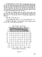
is depicted in Figure 9. The SECE approach also permits an enhancement of the conversion
thanks to a voltage increase and a reduction of the time shift between voltage and velocity, and
allows a typical energy gain of 3.5 compared to the maximal harvested energy in the standard
case under constant displacement magnitude.
Nevertheless, the SECE techniques does not allow controlling the trade-off between extracted
energy and conversion improvement, as all the energy on the active material is extracted. The
principles of the technique may be enhanced by combining the series SSHI approach with the
SECE, leading to the DSSH technique (Lallart et al., 2008a). This scheme, depicted in Figure 10,
consists in first extracting a part of the electrostatic energy on the piezoelectric or pyroelectric
material on an intermediate capacitor C
int
, while the remaining energy is used to perform
the voltage inversion leading to the conversion magnification. Then the energy available on
the intermediate capacitor is transferred to the load in the same way than the SECE. Hence,
through the ratio between the active element capacitance and intermediate capacitance, it is
possible to finely control the trade-off between extracted energy and conversion enhancement,
allowing a typical harvested energy 7.5 higher than the maximal harvested energy in the
Type Impedance Efficiency
Step-down (Ottman, Hofmann and Lesieutre, 2003)
2Lf
sw
δ
2
1
1−
V
out
V
in
65%
Buck-boost (Lefeuvre et al., 2007a)
2Lf
sw
δ
2
75%
Table 4. Impedance matching systems (V
out
and V
in
refer to output and input voltages)
Fig. 9. SECE technique
3
As the optimal load depends on the frequency, broadband energy harvesting is quite delicate for these
architectures.
104
Ferroelectrics - Applications
Ferroelectric Materials for Small-Scale Energy Harvesting Devices and Green Energy Products 11
Fig. 10. DSSH technique
standard case under constant displacement magnitude or constant temperature variation
magnitude and independent from the connected load. The SECE and DSSH techniques have
also the advantage of being able to harvest energy even for low load values, while in the case
of low frequency (typical for temperature variation), the optimal load for the standard and
SSHI approaches would be very large.
When taking into account the damping effect caused by the backward coupling in the case of
mechanical energy harvesting using piezoelectric principles, the harvested energy using the
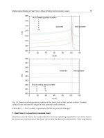
SECE and DSSH techniques is given in Table 5 and depicted in Figure 11.
Figure 11 shows the effectiveness of the techniques for allowing a significant power output
even for low values of the figure of merit k
2
Q
M
, especially for the DSSH approach, which
permits the same power output than the standard technique with 10 times less active
materials. Contrarily to the SECE technique, the DSSH does not present a decreasing
power for large values of k
2
Q
M
as the intermediate capacitor also permits controlling
the trade-off between extracted energy and damping effect (or equivalently the backward
coupling between energy conversion stage and host structure). It can be noted that, due to
the losses in the inductance during the energy transfer process, the power limit is decreased.
Technique Harvested energy
SECE γ
C
2
π
k
2
Q
M
(
1+
4
π
k
2
Q
M
)
2
F
M
2
C
DSSH
4
γ
C
2πk
2
Q
M
(
1−γ
)
2
(
π
(
1−γ
)
+
4k
2
Q
M
(
1+γ
))
2
F
M
2
C
for k
2
Q
M
≤
4
π
1
−γ
1+γ
γ
C
F
M
2
8C
for k
2
Q
M
≥
4
π
1
−γ
1+γ
Table 5. Harvested energies for SECE and DSSH techniques under constant force magnitude
(γ
C
refers to the energy transfer efficiency)
Fig. 11. Harvested energy for the SECE and DSSH techniques (γ
C
= 0.9)
4
for the optimal intermediate capacitance value
105
Ferroelectric Materials for Small-Scale Energy Harvesting Devices and Green Energy Products
12 Feroelectrics Vol. IV: Applications
However, this statement has to be weighted by the fact that classical and SSHI approaches
require load adaptation stages, whose effectiveness is usually less than 80%. Hence, the
power limit of the SECE and DSSH schemes is similar to the one obtained with the other
techniques featuring load adaptation stages. Such a statement also applies for constant
vibration magnitude or constant temperature variation magnitude case. Finally, it can be
noted that the power transfer from the intermediate capacitor to the load can also be controlled
by fixing a voltage threshold value, leading to the concept of Enhanced Synchronized Switch
Harvesting (ESSH) described by Shen et al. (2010).
6. Implementation considerations
Now the general principles of energy harvesting exposed, it is proposed in this section to
discuss about their implementation for the design of realistic self-powered devices.
The first issue that may arise for the use of nonlinear techniques is the control of the switching
device. Actually, the minimum and maximum detection can be done by comparing the
voltage across the active material with its delayed version. The maximum is then detected
when the delayed signal is greater than the original one (Lallart et al., 2008b; Liang and Liao,
2009; Qiu et al., 2009; Richard, Guyomar and Lefeuvre, 2007). The self-powered autonomous
switching device based on this principles therefore consumes very little power, typically
less than 5% than the electrostatic energy available on the ferroelectric material, therefore
not compromising the energy harvesting gain. The implementation of the self-powered
switch, depicted in Figure 12, also shows that only typical electronic components are required,
allowing an easy integration of the device.
Another point of interest when designing realistic energy harvesters is the incoming
solicitation. While sine excitation is usually considered for theoretical analysis, realistic
systems would be more likely subjected to random input (Blystad, Halvorsen and Husa,
2010b; Halvorsen, 2008). Although very few studies addressed this problem in the case of
nonlinear energy harvesting (Badel et al., 2005; Lallart, Inman and Guyomar, 2010g; Lefeuvre
et al., 2007b), it can be stated that load independent techniques (SECE, DSSH and ESSH) would
be more suitable under such circumstance, as the optimal load is frequency-dependent for the
other approaches.
Fig. 12. Principles of the self-powered switch for maximum detection (the minimum
detection is simply obtained by reversing the polarity of the system)
106
Ferroelectrics - Applications
Ferroelectric Materials for Small-Scale Energy Harvesting Devices and Green Energy Products 13
Finally, one of the most promising applications of ferroelectric materials used for energy
harvesting lies in the MEMS
5
scale. However, when dealing with electroactive microsystems,
the output voltage that can be expected is quite low. This may be a serious issue when dealing
with energy harvesting as energy harvesting interfaces feature discrete components such
as diodes or transistors that present voltage gaps due to their semiconductor nature, hence
compromising the operations of the microgenerators. In order to counteract this drawbacks,
it is possible to replace the inductance of the series SSHI by a transformer in order to divide
the threshold voltage of diodes seen by the piezoelectric element (Garbuio et al., 2009), or to
use mechanical rectifiers (Nagasawa et al., 2008).
7. Application examples
In this section two examples of self-powered devices will be exposed, demonstrating the
possibility of designing systems powered up by their close environment. However, a careful
attention has to be placed on the power management strategy, in order to have a positive
energy balance between harvested energy and supplied energy. Some general design rules
can be considered for saving energy:
• Use sleep modes as much as possible.
• Optimize components that require the highest energy per operating cycle, rather than
devices consuming the highest power. For example, a system that consumes 1 mW for
10 μs (hence necessitating 10 nJ) is therefore less critical than a device requiring 10 μW for
1 s, as the associated energy per cycle of the latter is 10 μJ.
• Re-think the processes to minimize the energy.
7.1 Self-powered accelerometer
The first proposed application example is a self-powered accelerometer. The system is
composed by a SSHI energy harvesting device, a microcontroller (for power management,
data acquisition and communication management), a low-power accelerometer followed by a
filter to obtain the average acceleration and a RF module for data transmission (Figure 13).
When the harvested energy is sufficient (approximately 1 mJ), the microcontroller wakes up
and enables the accelerometer as well as the RF transmission module. After a predefined
wake-up time, the filtered output signal of the latter is digitized by the microcontroller.
The measurement results are then sent by RF transmission together with an identifier. The
accelerometer and RF module are finally turned off and the microcontroller enters in sleep
Fig. 13. Architecture of the self-powered accelerometer
5
Micro Electro-Mechanical Systems
107
Ferroelectric Materials for Small-Scale Energy Harvesting Devices and Green Energy Products
14 Feroelectrics Vol. IV: Applications
mode. If the energy is still sufficient, a new cycle is repeated after a given time period
(typically 10 s). The obtained waveforms using this device are depicted in Figure 14.
7.2 Self-powered SHM system
The second autonomous, self-powered wireless system presented in this section lies in a in-situ
structural condition monitoring system (Figure 15), which consists in analyzing the interaction
of an acoustic wave (Lamb wave) with the host structure (Guyomar et al., 2007; Lallart et al.,
2008c). The device is made of two self-powered components (Figure 16):
• The Autonomous Wireless Transmitter (AWT), which consists in harvesting energy with the
SSH module, and when the latter is sufficient, a microcontroller wakes up and applies a
pulse voltage on a additional piezoelectric element, which therefore generates the Lamb
wave. Then the AWT sends a RF signal containing its identifier for time and space
localization before entering into sleep mode for a given time period.
• The Autonomous Wireless Receiver (AWR), which also includes a SSHI system. The
AWR features a RF listening module which wakes up the system when it senses a RF
Fig. 14. Waveforms of acceleration measurements and RF comunication
Fig. 15. Self-powered SHM system
108
Ferroelectrics - Applications
Ferroelectric Materials for Small-Scale Energy Harvesting Devices and Green Energy Products 15
(a) AWT (b) AWR
Fig. 16. Structures of the self-powered SHM subsystems
communication incoming from a close AWT. Once woken up, the Lamb wave signature
is sensed, amplified, and its RMS value computed. This value is then compared to a
reference value (obtained in the pristine case), allowing the estimation of the change in
the mechanical structure. The results are then sent by RF transmission together with an
identifier. Once these operations terminated, the whole system enters into sleep mode.
After a predefined time period, the RF listening module is enabled to detect a new
inspection cycle.
In addition, an externally powered base station is used to gather the data. A summary of
the communication within the network is depicted in Figure 17 and the energy balance of the
system as a function of the stress within the structure is presented in Table 6. The energy
consumption estimation for the AWT and AWR are given by:
AWT :
- Microcontroller wake-up: 0.8 mJ
- RF emission: 0.2 mJ
- Lamb wave emission: 0.2 mJ
Total: 1.20 mJ
AWR :
- Microcontroller wake-up: 0.8 mJ
- RF listening: 0.6 mJ (average listening time: 3 s)
- Damage Index computation: 0.03 mJ
- RF emission: 0.25 mJ
Total: 1.68 mJ
According to Table 6, the system can operate as soon as the stress reaches 2 MPa, which
is a realistic stress value in classical structures. It can also be noted that the AWR energy
scavenging device features higher global coupling coefficient than the AWT, allowing to
harvest more energy in a given time period.
The damage detection estimation has been investigated by adding an artificial damage
consisting in a small mass of putty on the structure. Waveforms depicted in Figure 18
demonstrate the ability of the proposed system for quantitatively detecting the change in the
structural condition.
109
Ferroelectric Materials for Small-Scale Energy Harvesting Devices and Green Energy Products
16 Feroelectrics Vol. IV: Applications
Fig. 17. Communication network for the self-powerd SHM system
Stress (MPa) 1.5 1.75 2 2.25 2.5 3 3.5
Harvested energy in 10 s (mJ) for the AWT 0.77 1.05 1.36 1.72 2.13 3.06 4.17
Harvested energy in 10 s (mJ) for the AWR 1.10 1.5 1.96 2.48 3.06 4.41 6.00
Energy balance (mJ) for the AWT
−0.43 −0.15 0.16 0.52 0.93 1.86 2.97
Energy balance (mJ) for the AWR
−0.58 −0.18 0.28 0.80 1.38 2.73 4.32
Table 6. Energy balance for the self-powered wireless SHM device
Fig. 18. Results of the self-powered SHM system under artificial damage.
110
Ferroelectrics - Applications
Ferroelectric Materials for Small-Scale Energy Harvesting Devices and Green Energy Products 17
8. Conclusion
This chapter exposed the application of ferroelectric materials to small-scale energy
scavenging devices and self-powered systems, with a special focus on vibrations and
temperature variations, as ferroelectric devices present high energy densities and promising
integration potentials. From the analysis of the global energy transfer chain from the
energy source to the device to power up, it has been shown that the design of efficient
microgenerators has to be done in a global manner rather than optimizing each block
independently, because of backward couplings to may modify the behavior of previous
stages. Then several ways for improving the performance of energy harvesters have been
explored, showing that the use of nonlinear approaches may significantly increase the energy
conversion abilities and/or the independency from the connected device. Fundamental issues
such as realistic implementation, performance under real excitation and microscale design
have then been discussed. Finally, the possibility of designing truly self-powered wireless
systems has been demonstrated through two working application examples, showing that the
spreading of devices powered up by energy harvested from their close environment is now
only a question of time.
9. References
Andò, B.; Baglio, S.; Trigona, C.; Dumas, N.; Latorre, L. & Nouet, P. (2010). Nonlinear
mechanism in MEMS devices for energy harvesting applications. Smart Mater. Struct.,
Vol. 20, 125020.
Anton, S. R. & Sodano H. A. (2007). A review of power harvesting using piezoelectric materials
(2003-2006). Smart Mater. Struct., Vol. 16(3), R1-R21.
Badel, A.; Guyomar, D.; Lefeuvre, E. & Richard, C. (2005). Efficiency Enhancement of a
Piezoelectric Energy Harvesting Device in Pulsed Operation by Synchronous Charge
Inversion. J. Intell. Mater. Syst. Struct., Vol. 16, 889-901.
Badel, A.; Benayad, A.; Lefeuvre, E.; Lebrun, L.; Richard, C. & Guyomar, D. (2006a).
Single Crystals and Nonlinear Process for Outstanding Vibration Powered Electrical
Generators. IEEE Trans. on Ultrason., Ferroelect., Freq. Contr., Vol. 53, 673-684.
Badel, A.; Lagache, M.; Guyomar, D.; Lefeuvre, E. & Richard, C. (2007). Finite Element and
Simple Lumped Modeling for Flexural Nonlinear Semi-passive Damping. J. Intell.
Mater. Syst. Struct., Vol. 18, 727-742.
Beeby, S. P.; M. J.; & White, N. M. (2006). Energy harvesting vibration sources for microsystems
applications, Meas. Sci. Technol., Vol. 17, R175-R195.
Blystad, L C. J. & Halvorsen, E. (2010a). A piezoelectric energy harvester with a mechanical
end stop on one side. Microsyst. Technol., in press - available online. DOI: DOI:
10.1007/s00542-010-1163-0.
Blystad, L C. J.; Halvorsen, E. & Husa, S. (2010b). Piezoelectric MEMS energy harvesting
systems driven by harmonic and random vibrations. IEEE Trans. Ultrason., Ferroelect.,
Freq. Contr., Vol. 57(4), 908-919.
Challa, V. R.; Prasad, M. G.; Shi, Y. & Fisher, F. T. (2008). A vibration energy harvesting
device with bidirectional resonance frequency tunability. Smart Mater. Struct., Vol. 17,
015035.
Erturk A. & D. J. Inman (2008). Issues in mathematical modeling of piezoelectric energy
harvesters. Smart Mater. Struct., Vol. 17, 065016.
111
Ferroelectric Materials for Small-Scale Energy Harvesting Devices and Green Energy Products
18 Feroelectrics Vol. IV: Applications
Erturk A.; Hoffmann, J. & D. J. Inman (2010). A piezomagnetoelastic structure for broadband
vibration energy harvesting. Appl. Phys. Lett., Vol. 94, 254102.
Garbuio, L.; Lallart, M.; Guyomar, D. & Richard, C. (2009). Mechanical Energy Harvester with
Ultra-Low Threshold Rectification Based on SSHI Non-Linear Technique, IEEE Trans.
Indus. Elec., Vol. 56(4), 048-1056.
Guyomar, D.; Badel, A.; Lefeuvre, E. & Richard, C. (2005). Towards energy harvesting using
active materials and conversion improvement by nonlinear processing, IEEE Trans.
Ultrason., Ferroelect., Freq. Contr., Vol. 52, 584-595.
Guyomar, D.; Jayet, Y.; Petit, L.; Lefeuvre, E.; Monnier, T.; Richard, C. & Lallart, M.
(2007). Synchronized Switch Harvesting applied to Self-Powered Smart Systems :
Piezoactive Microgenerators for Autonomous Wireless Transmitters, Sens. Act. A:
Phys., Vol. 138, No. 1, 151-160.
Guyomar, D.; Pruvost, S. & Sebald, G. (2008). Energy Harvesting Based on FE-FE Transition in
Ferroelectric Single Crystals, IEEE Trans. Ultrason., Ferroelect., Freq. Contr., Vol. 55(2),
279-285.
Guyomar, D.; Sébald, G.; Pruvost, S.; Lallart, M.; Khodayari, A. & Richard, C. (2009). Energy
Harvesting From Ambient Vibrations and Heat, J. Intell. Mater. Syst. Struct., Vol. 20(5),
609-624.
Guyomar, D. & Lallart, M. (2011). Switching loss reduction in Nonlinear Piezoelectric
Conversion under Pulsed Loading, IEEE Trans. Ultrason., Ferroelect., Freq. Contr.,
Vol. 58(3), 494-502.
Halvorsen, E. (2008). Energy Harvesters Driven by Broadband Random Vibrations. J.
Microelectromech. Syst., Vol. 17(5), 1061-1071.
Han, J.; Von-Jouanne,A.; Le, T.; Mayaram, K. & Fiez, T. S. (2004). Novel power conditioning
circuits for piezoelectric micro power generators. In Proc. IEEE Appl. Power Electron.
Conf. Expo. (APEC), vol. 3, 1541-1546.
Hudak, N. S. & Amatucci, G. G. (2008). Small-scale energy harvesting through thermoelectric,
vibration, and radiofrequency power conversion. Appl. Phys. Rev., Vol. 103, 101301.
Jia, D. & Liu, J (2009). Human power-based energy harvesting strategies for mobile electronic
devices. Front. Energy Power Eng. China, Vol. 3(1), 27
˝
U46.
Keawboonchuay , C. & Engel, T. G. (2003). Electrical power generation characteristics of
piezoelectric generator under quasi-static and dynamic stress conditions. IEEE Trans.
Ultrason., Ferroelect., Freq. Contr., Vol. 50, 1377-1382.
Khodayari, A.; Pruvost, S.; Sebald, G.; Guyomar, D. & Mohammadi, S. (2009). Nonlinear
Pyroelectric Energy Harvesting from Relaxor Single Crystals. IEEE Trans. Ultrason.,
Ferroelect., Freq. Contr., Vol. 56(4), 693-699.
Krikke, J. (2005). Sunrise for energy harvesting products. IEEE Pervasive Comput., Vol. 4, 4-35.
Lallart, M.; Garbuio, L.; Petit, L.; Richard, C. & Guyomar, D. (2008a) Double Synchronized
Switch Harvesting (DSSH) : A New Energy Harvesting Scheme for Efficient Energy
Extraction, IEEE Trans. Ultrason., Ferroelect., Freq. Contr., Vol. 55,(10), 2119-2130.
Lallart, M.; Lefeuvre, E.; Richard, C. & Guyomar, D. (2008b). Self-Powered Circuit for
Broadband, Multimodal Piezoelectric Vibration Control. Sens. Act. A: Phys., Vol. 143,
No. 2, 277-382, 2008.
Lallart, M.; Guyomar, D.; Jayet, Y.; Petit, L.; Lefeuvre, E.; Monnier, T.; Guy, P. & Richard,
C. (2008c). Synchronized Switch Harvesting applied to Selfpowered Smart Systems:
Piezoactive Microgenerators for Autonomous Wireless Receiver, Sens. Act. A: Phys.,
Vol. 147, No. 1, 263-272.
112
Ferroelectrics - Applications
Ferroelectric Materials for Small-Scale Energy Harvesting Devices and Green Energy Products 19
Lallart, M. (2010a). Conversion électroactive et application aux systèmes auto-alimentés
6
.
Editions Universitaires Européennes, in french. ISBN: 978-613-1-50507-2
Lallart, M.; Anton, S. R. & Inman, D. J. (2010b). Frequency Self-tuning Scheme for Broadband
Vibration Energy Harvesting. J. Intell. Mat. Syst. Struct., Vol. 21(9), 897-906 .
Lallart, M.; Guyomar, D.; Richard, C. & Petit, L. (2010c). Nonlinear optimization of acoustic
energy harvesting using piezoelectric devices. J. Acoust. Soc. Am., Vol. 128(5),
2739-2748.
Lallart, M.; Garbuio, L; Richard, C. & Guyomar, D. (2010d). High Efficiency, Low-Cost
Capacitor Voltage Inverter for Outstanding Performances in Piezoelectric Energy
Harvesting, IEEE Trans. on Ultrason., Ferroelect., Freq. Contr., Vol. 57(2), 281-291.
Lallart, M. & Guyomar, D. (2010e). Piezoelectric conversion and energy harvesting
enhancement by initial energy injection. Appl. Phys. Lett., Vol. 97, # 014104.
Lallart, M. & Inman, D. J. (2010f). Low-Cost Integrable Tuning-Free Converter for Piezoelectric
Energy Harvesting Optimization. IEEE Trans. Power Electron., Vol. 25(7), 1811-1819.
Lallart, M.; Inman, D. J. & Guyomar, D. (2010g). Transient Performance of Energy Harvesting
Strategies under Constant Force Magnitude Excitation. J. Intell. Mater. Syst. Struct.,
Vol 21(13), 1279-1291.
Lefeuvre, E.; Badel, A.; Richard, C. & Guyomar, D. (2005). Piezoelectric energy harvesting
device optimization by synchronous electric charge extraction. J. Intell. Mat. Syst.
Struct., Vol. 16, No. 10, 865-876.
Lefeuvre, E.; Badel, A.; Richard, C.; Petit, L. & Guyomar, D. (2006). A comparison between
several vibration-powered piezoelectric generators for standalone systems, Sens. Act.
A: Phys, Vol. 126, 405-416.
Lefeuvre, E.; Audigier, D.; Richard, C. & Guyomar, D. (2007a). Buck-boost converter for
sensorless power optimization of piezoelectric energy harvester. IEEE Trans. Power
Electron., Vol. 22(5), 2018-2025.
Lefeuvre, E.; Badel, A.; Richard, C. & Guyomar, D. (2007b). Energy harvesting using
piezoelectric materials: Case of random vibrations. J. Electrocem., Vol. 19(4), 349-355.
Lesieutre, G. A.; G.K. Ottman, G. K. & Hofmann, H. F. (2003). Damping as a result of
piezoelectric energy harvesting. J. Sound Vib., Vol. 269(3-5), 991-1001.
Liang, J. R. & Liao, W. H. (2009). An Improved Self-Powered Switching Interface for
Piezoelectric Energy Harvesting. In Proc. of 2009 IEEE International Conference on
Information and Automation, 945-950.
Liu, Y.; Tian, G.; Wang, Y; Lin, J.; Zhang, Q. & Hofmann, H. F. (2009). Active Piezoelectric
Energy Harvesting: General Principles and Experimental Demonstration. J. Intell.
Mat. Syst. Struct., Vol. 20, 575-585.
Makihara, K.; Onoda, J. & Miyakawa, T. (2006). Low energy dissipation electric circuit for
energy harvesting. Smart Mater. Struct., Vol. 15, 1493-1498.
Nagasawa, S.; Suzuki, T.; Takayama, Y.; Tsuji, K. & Kuwano, H. (2008). Mechanical rectifier for
micro electric generators. IEEE 21st International Conference on Micro Electro Mechanical
Systems, Tucson, AZ, USA, January 2008, 992-995.
Ottman, G. K.; Hofmann, H. F.; Bhatt, A. C. & Lesieutre, G. A. (2002). Adaptive Piezoelectric
Energy Harvesting Circuit for Wireless Remote Power Supply. IEEE Trans. Power
Electron., vol. 17(5), 669-676.
6
Electroactive conversion and application to self-powered systems
113
Ferroelectric Materials for Small-Scale Energy Harvesting Devices and Green Energy Products
20 Feroelectrics Vol. IV: Applications
Ottman, T. S.; Hofmann, H. F. & Lesieutre, G. A. (2003). Optimized piezoelectric energy
harvesting circuit using step-down converter in discontinuous conduction mode.
IEEE Trans. Power Electron., Vol. 18(2), 696-703.
Paradiso, J. A. & Starner, T. (2005). Energy scavenging for mobile and wireless electronics.
IEEE Pervasive Computing, Vol. 4, 18-27.
Park, S E. & Hackenberger, W. (2002). High performance single crystals, applications and
issues. Current Opinion in Solid State and Material Science, Vol. 6, 11-18.
Qiu, J.; Jiang, H.; Ji, H. & Zhu, K. (2009). Comparison between four piezoelectric energy
harvesting circuits. Front. Mech. Eng. China, Vol. 4(2), 153-159.
Rakbamrung, P.; Lallart, M.; Guyomar, D.; Muensit, N.; Thanachayanont, C.; Lucat, C.;
Guiffard, B.; Petit, L. & Sukwisut, P. (2010). Performance Comparison of PZT And
PMN-PT Piezoceramics for Vibration Energy Harvesting. Sens. Act. A: Phys., Vol. 163,
493-500.
Richard C.; Guyomar, D. & Lefeuvre, E. (2007). Self-Powered Electronic Breaker With
Automatic Switching By Detecting Maxima Or Minima Of Potential Difference
Between Its Power Electrodes, patent # PCT/FR2005/003000, publication number:
WO/2007/063194, 2007.
Roundy, S.; Wright, P. K. & Rabaey, J. (2003). A study of low level vibrations as a power source
for wireless sensor nodes. Comp. Comm., Vol. 26, 1131-1144.
Shahruz, S. M. (2006). Design of mechanical band-pass filters for energy scavenging. J. Sound
Vib., Vol. 292, 987-998.
Shen, H.; Qiu, J.; Ji, H.; Zhu, K. & Balsi, M. (2010). Enhanced synchronized switch harvesting:
a new energy harvesting scheme for efficient energy extraction. Smart Mater. Struct.,
Vol. 20, 115017.
Shu, Y. C.; Lien, I. C. & Wu, W. J. (2007). An improved analysis of the SSHI interface in
piezoelectric energy harvesting. Smart Mater. Struct., Vol. 16, 2253-2264.
Soliman, M. S. M.; Abdel-Rahman, E. M.; El-Saadany, E. F.& Mansour, R. R. (2008). A
wideband vibration-based energy harvester. J. Micromech. Microeng., Vol 18, 115021.
Sun, C.; Qin, L.; Li, F.; Wang, Q M. (2009). Piezoelectric Energy Harvesting using Single
Crystal Pb
(Mg
1/3
Nb
2/3
)O
3
− xPbTiO
3
(PMN-PT) Device. J. Intell. Mat. Syst. Struct.,
Vol. 20(5), 559-568.
Taylor, G. W.; Burns, J. R.; Kammann, S. M.; Powers, W. B. & Welsh, T. R. (2001). The Energy
Harvesting Eel: A Small Subsurface Ocean/River Power Generator. IEEE J. Oceanic
Eng., Vol. 26, 539-547.
Vullers, R.J.M.; van Schaijk, R.; Doms, I.; Van Hoof, C. & R. Mertens (2009). Micropower energy
harvesting. Solid-State Electronics, Vol. 53, 684-693.
Zhu, D.; Tudor, M. J. & Beeby, S. P. (2010). Strategies for increasing the operating frequency
range of vibration energy harvesters: a review. Meas. Sci. Technol., Vol. 21, 022001.
Zhu, H.; Pruvost, S.; Guyomar, D. & Khodayari, A. (2009). Thermal energy harvesting
from Pb
(
Zn
1/3
Nb
2/3
)
0.955
Ti
0.045
O
3
single crystals phase transitions. J. Appl. Phys.,
Vol. 106, 124102.
114
Ferroelectrics - Applications
Part 2
Memories
6
Future Memory Technology and Ferroelectric
Memory as an Ultimate Memory Solution
Kinam Kim and Dong Jin Jung
Samsung Electronics,
S. Korea
1. Introduction
Silicon industries have notched up notable achievements of computer-related technology
over the past two decades, leading to rapid progression in information technology (IT). As a
result of such a great improvement in IT applications, it is now not unusual to find mobile
applications such as personal digital assistants, mobile phones with digital cameras, smart
phones, smart pads able to access the Internet and hand-held personal computers. These
mobile applications currently require an array of single-functioned conventional memories
as they are not sufficient individually in functionality, but must combine their separate
functions.
For example, dynamic random access memory (DRAM) is capable of processing massive
amounts of data speedily (e.g., main memory in personal computers and servers). DRAM is
highly scalable (several gigabit are commonly accessible), but requires lots of power
consumption even in stand-by mode (~10
-3
Ampere) because of the necessity of refreshing
cycles in its operation. By contrast, static random access memory (SRAM) saves power
1
because its stand-by current is a few micro-Amperes. The demerit of SRAM is not readily to
make it high density. This is due to the fact that its unit memory element consists of four
complementary metal-oxide-semiconductor (CMOS) transistors along with two
conventional transistors. SRAM’s cost-benefit ratio is too high because the 6 components
need much more area per unit bit memory. Data retention of both DRAM and SRAM is
volatile in bit-storing nature when power goes off. In contrast to these two memories, flash
memory is non-volatile. However, operation voltage during either write or erase on flash
memory is too high to use the raw voltage-level of power input, Vcc (the term of Vcc comes
from collector to collector voltage in a bipolar transistor). Thus during the write or erase
operation, internal dummy operation (so called “charge pump”) are used to pump up the
input power Vcc to 5 times more than Vcc level; this is crucial in flash memory devices due
to imbalance of read and write energy. The reason why the memory needs to boost the
write/erase voltage up to such a high level is that hot carriers, e.g., high energy electrons,
are forced to be injected through tunnel oxide to a floating gate of the transistor structure.
As a result, there are two kinds of performance restrictions for use of IT applications.
Writing speed of flash memory is not fast enough of an order of several milliseconds. That
1
This is not necessarily true because the stand-by current of SRAM begins to exceed DRAM’s in a deep
sub micron scale due to involvement of high field junction.
Ferroelectrics - Applications
118
makes the erasing speed of the device to be in the range of tenths of seconds. Another
drawback of the device is endurance, which is defined as cycle times to write data in a
memory cell. Generally, while write endurance of DRAM and SRAM is more than 10
15
cycle
2
(10
15
corresponds to equivalent 10 years for use), flash memory has approximately 10
6
cycles
at most as writing endurance. In addition to flash memory, there is another non-volatile
memory, so called electrically erasable and programmable read only memory (EEPROM).
However, EEPROM has the same limitations in flash memory due to structural and
operational similarity of the unit memory cell in flash memory.
To compensate for the aforementioned disadvantages of conventional memory devices,
mobile applications in the IT world have adopted a combination of individual memories,
which give several penalties such as a large volume of space to pack them all and complex
time adjustments to synchronize them as well. As needs of IT technology are pushing
forward to many functional requirements including much faster Internet access and far
more image processing, this combining approach has a limitation to apply them to those for
mobile uses. Therefore, it is strongly desirable to develop an ultimate memory solution as a
single memory platform, possessing positive features of the individual memories but
excluding their disadvantages. The feature of the ideal memory should have fast operation
for speedy communication, high density for massive data-processing, non-volatility and low
power consumption for portable applications.
Among many candidates of ideal memory devices, a memory device to use ferroelectric
properties, so called ferroelectric random access memory (FRAM), was proposed and
experimentally explored in terms of 512-bit memory density (Evans & Womack, 1988). This is
because its functional feature is similar to that of an ideal memory. This is thanks to the bi-
stable state of ferroelectrics at near ambient temperature. There are several important
characteristics worth mentioning. First, since core circuitry for the memory does not require
stand-by power during quiescent state and the information remains unchanged even with no
power supplied, it is thus non-volatile. Second, configuration of unit memory element is similar
to that either of flash or of DRAM, allowing it to potentially become cost-effective high density
memory. Third, speed of ferroelectric memory could be very close to those of the conventional
volatile memories such as DRAM and SRAM. This is, in practice, because repeating the
polarization reversal-read and write operation, does not need boost up base voltage unlike
flash memory, stemming from balance of read and write energy of the same order of
magnitude (Kryder & Kim, 2009). A good example of this is that, according to literature
published recently, one of the FRAMs as a non-volatile memory has attractive memory
performance such as fast access time of 1.6 GB/sec, negligible stand-by current of less than 10
micro-Ampere, and low voltage operation of less than 2.0 V even in read and write action
without erase operation (Shiga et al., 2009; Jung et al., 2008). Since then, there have been
tremendous improvements in FRAM developments, migrating from sub-micron to nano scale
in technology node. As such, this chapter is categorized into two: First demonstrates
2
Provided a clock frequency f of a microprocessor in an embedded system is 20 MHz (the fastest one in
2006 is about 5 MHz), reference counts necessary for cycle times per a year, is less than 1E13 in spite of
considering 2% of strong data-locality in data memory. Note, the reference counts per a second is
proportional to the products of frL, where f is a clock frequency, r is ratio of number of cycles in read
and write operation to unit cycle and L is a constant of representing data-access locality. We will discuss
this more in section 3.2.
Future Memory Technology and Ferroelectric Memory as an Ultimate Memory Solution
119
reminiscent of how memory technologies penetrate technological barriers to match the
Moore’s law. Also, authors are here trying to give an insight of how silicon technology can
evolve even in 20-30 nm technology node. Second is devoted to ferroelectric memories as an
ultimate memory solution in many aspects such as lifetime data-retention and endurance; size
effects; integration technologies; and feasibility as a fusion memory element.
2. Future memory technology
2.1 Evolution of silicon technology
2.1.1 Moore’s law
It is generally accepted that semiconductor industry will continue to expand rapidly due to
steady growth of the mobile, digital consumer and entertainment markets. In addition to
these, many more growth engines will appear, encompassing the automotive, information-
technology, biotechnology, health, robotic and aerospace industries. The advances in silicon
technology that has been the backbone of tremendous previous growth, were foreseen in
1965 when Gordon Moore published his famous prediction about the constant growth rate
of chip complexity (Moore, 1965). And, in fact, it has repeatedly been shown that the
number of transistors integrated into silicon chips has indeed doubled every 18 months.
Increases in packing density, according to the Moore’s law, are driven by two factors:
reductions in production costs and increases in chip performance. Another prominent
example of the unstoppable pace of technology advancement
3
, has been predicted (Hwang,
2006). Figure 1 shows Moore’s doubling phenomena of the number of components−the
number of gate in case of CPU (central processing unit) and density in memory device.
Fig. 1. Moore’s doubling phenomena of the number of chips (Moore, 2006).
3
Moore’s law was predicted to stagnate to the end of the 20th century, but new sources of momentum
are able to maintain or acclerate a growth trend. SoC (System-on-a-chip) integration has the potential to
continue IC (integrated-circuit) cost reduction and to perpetrate growth of personal Internet products.
Ferroelectrics - Applications
120
Despite these bright prospects, there is growing concern about whether semiconductor
technology can continue to keep pace with demand when silicon technology enters the
“deep nano-scale” dimension. This is because there are limits to transistor scaling, and
narrowing margins in manufacturing due to ever-increasing fabrication costs tied to
technical complexities (Kim & Jeong, 2005; Kim & Choi, 2006). The manufacturing cost
grows because the engineering becomes more complex as transistors shrink in size. The
scale is staggering, but the current generation of memory chips is 30 nm node across. This
does mean that innovation is more process driven, and may require suppliers to think about
what customers need and value, rather than simply pushing for ever greater density of
transistors. Though most experts believe that silicon technology will maintain its leadership
down to 20 nm, beyond this node a number of fundamental and application-specific
obstacles will prevent further shrinkage. A common example is the inevitable occurrence of
variations due to rough line edges and surfaces when pattern sizes approach atomic scales
(Hwang, 2006). It is therefore the primary aim of this section to present various possible
paths to overcome these obstacles and eventually to maintain the technology-scaling trend
beyond 20 nm node.
As will be shown, these solutions include not only 3-D (three-dimensional) technologies but
also non-silicon technologies on a molecular scale. In addition, new applications, and new
growth engines for the semiconductor industry will be provided from a combination of
separate technologies such as silicon-based IT with new materials (Whang et al., 2003;
Wada, 2002). Therefore, this section is structured as follows: First, a review of the evolution
of key silicon technologies is given. Next, we discuss scaling limits in each technology node
and demonstrate practical and plausible solutions to penetrate these scaling barriers. Both
DRAM and NAND flash memory are dealt with in discussion. And then, authors present
prospects for the future silicon industry covering fusion technologies.
2.1.2 Evolution of silicon technology
DRAM: Since the first 1,024-bit DRAM was demonstrated by Intel
TM
in the early 1970’s, the
highest available density of DRAM has doubled every 18 months. Now DRAM technology has
reached 30 nm in process technology and 4 Gb in density, which will be deployed soon in the
marketplace. Further, 20-nm DRAM is being developed at R&D centers around the world.
DRAM technology has evolved toward meeting a need for ever-increasing demand both of
data retention and of performance improvements. Increases in data retention impose great
challenges on DRAM technology by requiring not just a sufficient amount of capacitance in a
memory cell but an extremely low level of leakage current from storage junction.
As device shrinks, it has been being one of the most challenging to achieve an adequate
amount of cell capacitance in DRAM. It is widely agreed that the value of cell capacitance is
more than 20 fF, regardless of technology-node migration. This is because sensing signal
developed from memory cells, is vulnerable to become interfered by unwanted noise factors
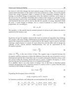
according to its operational nature. Sensing signal, Vs can be expressed by equation (1),
where C
S
is cell capacitance at storage node; C
BL
is parasitic bit-line capacitance; AIVC is cell
array internal voltage; and the last term V
UN
is undesirable noise. In equation (2), the first
term I
LEAK
t
REF
in the parenthesis is a term of charge loss due to junction leakage current,
I
JUNC
; gate-induced-drain-leakage (GIDL) current, I
GIDL
; and non-generic leakage current, I
NG
,
arising from integration imperfections (e.g., dielectric leakage current and cell-to-cell
leakage current) as indicated in equation (3).
Future Memory Technology and Ferroelectric Memory as an Ultimate Memory Solution
121
2
·
1
1
2
3
All of those loss factors are constituents of data-retention time, so called refresh time, t
REF
.
V
N
is noise voltage due both to noise coupling and to mis-matches of threshold voltage and
conductance of sense amplifiers. Another source of charge loss, Q
I
in Eq. (2) has to be
considered when DRAM is exposed to irradiations such as -particle and cosmic rays. These
undesirable components are very difficult to attenuate and become dominant as device
dimensions are smaller. To maintain almost non-scalable requirement of cell capacitance of
more than 20 fF/cell, dielectric material of cell capacitors have continuously evolved into
high-
κ
dielectric materials and at the same time their structures have been pursued actively
for novel ones (Lee et al., 2003a; Kim et al., 2004a). This is due to the fact that cell capacitor
area decreases by a factor
4
of 1/k ~ 1/k
2
as technology scales, where k denotes a scaling
factor, where k > 1 (See Denard et al., 1974). In general, when designing device to a smaller
dimension, the device is scaled by a transformation in three variables: dimension, voltage,
and doping concentration. Firstly, all the linear dimensions are reduced by a unit-less
scaling constant k, e.g., t
OX
’ = t
OX
/k. Such reduction includes not only vertical dimensions
such as thickness of gate oxide and junction depth, but also horizontal dimensions, for
example, channel length L and width W. Secondly, voltage applied to the new device has to
be reduced by the same factor, e.g., V
CC
’=V
CC
/k. Lastly, doping concentration, N
A
is to be
increased, e.g., N
A
’ = k
⋅
N
A
.
In practice, DRAM’s capacitor has begun with a stacked 2-D (two-dimensional) structure,
integrated under bit-line in process architecture
5
until the mid 1990’s. Since then, DRAM has
changed in structure to have an integration scheme of cell-capacitors placed over bit-line
(COB) though there was an attempt to use trench-type capacitors, which are buried deeply
in silicon substrate. In the 1990’s, dielectric material of the cell capacitors has adopted
silicon-based dielectrics, SiO
2
/Si
3
N
4
, whose dielectric constant lies in between 3.9 and 7.0.
With these relatively low-
κ
dielectrics, a cell capacitor has headed for expanding its area as
much as possible. Thus, its structure has been transformed in substantially complex ways,
from a simple stack to a hemi-spherical-silicon-grain (HSG) stack, to a HSG cylinder until
the late 1990’s. The advent of high-
κ
dielectrics since the beginning of 21
st
century has
brought a new era of building the cell capacitors. Table 1 compares fundamental material
properties of high-
κ
candidates with those of conventional low-
κ
dielectrics. These high-
κ
dielectrics have allowed us to form the cell capacitors into simpler one-cylinder-stack (OCS)
than those in low-
κ
dielectrics due to relatively higher dielectric constant. Provided high-
κ
dielectric material utilizes, increase in cell capacitance will be achieved simply by increase in
height of a cylinder. Such an increase in height gives rise to skyrocketing of aspect ratio of
4
A scaling factor of capacitance C = εA/t is supposed to be 1/k in a 2-D stack structre, but since
capacitor thickness t is not a contraint factor any more in a 3-D structure, capacitance can be written in
1/k
2
.
5
So called capacitor-under-bit-line (CUB) in integration architecture.
Ferroelectrics - Applications
122
cell capacitors when technology scales, together with dramatic decrease in footprint. In
typical, an aspect ratio of cell capacitors ranges from 6 to 9 until 100 nm technology node. A
higher aspect ratio has brought another obstacle in building cell capacitors robust:
mechanical instability of OCS structures. As a result, many smart engineers in silicon
industries has introduced a novel capacitor structure, supporter-added OCS such as mesh
type cell capacitors, which can increase the cell capacitor height with desired mechanical
stability (Kim et al., 2004a). Taking into account the recent advances of the cell-capacitor
technology, the aspect ratio reaches 35 to 45, which is far beyond those of the world tallest
skyscrapers, ranging from 8.6 to 10.0.
Materials
Dielectric
constant (κ)
Band gap E
G
(eV)
Crystal Structure(s)
SiO
2
3.9 8.9 Amorphous
Si
3
N
4
7.0 5.1 Amorphous
Al
2
O
3
9.0 8.7 Amorphous
Y
2
O
3
15 5.6 Cubic
La
2
O
3
30 4.3 Hexagonal, cubic
Ta
2
O
5
26 4.5 Orthorhombic
TiO
2
80 3.5 Tetragonal, rutile, anatase
HfO
2
25 5.7 Monoclinic, tetragonal, cubic
ZrO
2
25 7.8 Monoclinic, tetragonal, cubic
Table 1. Comparison of material properties of high-
κ
dielectric candidates with those of
conventional low-
κ
dielectrics (Wilk et al., 2001).
In the meanwhile, charging and discharging properties of cell capacitors depend strongly on
performance of cell array transistors (CATs). On-current of the CAT plays a critical role in
its charging behaviors while off-leakage current of the CAT is a decisive factor to determine
their discharging characteristics. On the one hand, on-current (Ion) needs to be at least
greater than several 10
-6
Ampere to achieve reasonable read and write speed. On the other,
off-leakage current (Ioff) has to satisfy a level of 10
-16
Ampere to minimize charge loss just
after charging up the cell capacitors to ensure adequate sensing-signal margin as indicated
in Eq. (2). Despite continuation of technology migration, the ratio of Ion/Ioff has remained
constant to 10
10
approximately. CAT’s technology has evolved to meet this requirement.
·
·
·
2
,
4
where
μ
eff
is effective mobility for electrons, C
OX
is capacitance of gate oxide, W is width of
transistor’s active dimension, and L
eff
is effective channel length.
At first, from the structural point of view, 2-D planar-type CAT (PCAT) has been moved to
3-D CAT. The reason why 3-D CAT has been adopted is to relieve data retention time. In
100-nm technology node, L
eff
of the PCATs does not ensure a specific level of off-leakage
current requirement (less than 10
-15
A) due to high-field junction. The high electric field is
caused by high-doping concentration near the channel region to block short-channel-effect
(SCE). Under such a SCE circumstance, a transistor does not, in general, work any longer, by
a way of punch-through between source and drain when its channel length becomes shorter.
As denoted in Eq. (2) and (3), off-leakage currents I
LEAK
are closely related to data retention
Future Memory Technology and Ferroelectric Memory as an Ultimate Memory Solution
123
time. Generically this I
LEAK
arises from sub-threshold current and gate-induced drain
leakage (GIDL) current of cell array transistors along with junction leakage current from
storage node. As L
eff
is scaled down, the increased doping concentration against the SCE
strengthens electric field across storage node junction. This increase in junction-leakage
current results in degrading the data retention time (Kim et al., 1998). The degradation of
data retention time becomes significant below 100 nm node due to rapid increase in junction
electric field again (Kim & Jeong, 2005). This issue since the mid 2000’s has been overcome
by introducing 3-D cell transistors, where the junction electric-field can be greatly reduced
due to lightly doped channel. One example of these newly developed structures is RCAT
(Recess Channel Array Transistor) structure whose channel detours around a part of silicon
substrate so that the elongated channel can be embodied in the array transistor (Kim et al.,
2003). Also, the RCAT structure gives us another benefit, which lessens threshold voltage
(Vth) due to lower doping concentration. Thereby, not only does DRAM’s core circuitry
operate at lower voltage but also CAT’s on-current increases, as denoted in Eq. (4). Note
that, according to the Moore’s law, Vcc must be scaled down for power save. This trend has
continued to come to 60 nm technology node. However, beyond 60 nm of technology node,
on-current requirement has not been satisfied with such a RCAT approach alone. Thus,
further innovations since 50 nm node have been pursued in a way of a negative word-line
(NWL) scheme
6
in DRAM core circuitry. The NWL scheme compared with a conventional
ground-word-line (GWL) scheme, allows us Vth reduction further, which means more on-
current. However, another adverse effect on the CAT can occur as a result of the NWL. Since
CAT’s gate potential goes more negative during holding data stored at the storage junction,
from which GIDL current increases as a function of gate-storage voltage, level of which is as
high as that of gate potential compared with the conventional GWL. Many device engineers
have given much effort to tackle this problem and finally have figured it out by
technological implementation, for instance, mitigation of electric field exerted locally in the
region overlapped between source/drain and gate in the RCAT. In pursuit of purpose, gate
oxide needs to be different in thickness.
Provided that the oxide thickness in the overlapped region is thicker than that in the channel,
unwanted GIDL current will decrease in proportion to electric field of the overlapped zone in
the storage-node to gate (Lee et al., 2008; Jung et al., 2009). According to our calculation, one
can extend this NWL-based RCATs down to 40 nm node with minor modifications (Jung et al.,
2009). In 30 nm technology node, it becomes extremely difficult to achieve the successful
Ion/Ioff ratio. A report has shown that a body-tied FinFET (fin field-effect-transistor) as a cell
array transistor seems to be very promising due to its superb performances: excellent
immunity against the SCE; high trans-conductance; and small sub-threshold leakage (Lee et
al., 2004). For example, it allows us to have not only lower Vth but lower sub-threshold swing
due to a fin-gate structure, providing more width for on-current and wrapping the gate for Vth
and sub-threshold swing down. It is believed that the body-tied FinFET leads DRAM
technology to be extendable down to 30 nm node. In off-leakage current, CAT’s gate material
has been being transformed to metal gate of higher work function (4.2~4.9 eV) instead of n+
poly-silicon gate. The lower Vth coming from higher work function provides us with lower
channel doping. This leads to lower junction electric field and results in lower off-leakage
6
Since a level of dc (direct current) bias at unselected word-lines is negative, sub-threshold leakage
current of a cell transistor becomes extremely low because its channel has never chance to be on-set of
inversion, leading to keeping a reasonable level of off-leakage current despite low Vth.
Ferroelectrics - Applications
124
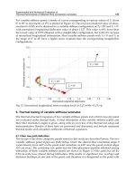
current. Figure 2 shows how DRAM’s CAT structure has evolved during the past decade.
Beyond 30 nm of technology node, a novel structure must be suggested for continuing the
successful Ion/Ioff ratio. Among many structures, a vertical channel CAT (VCAT) is one of the
good candidates (Yoon et al., 2006). This is because it can plausibly permit us to access an ideal
transistor. A VCAT has a surrounding gate buried in silicon substrate (Kim, 2010). Bit-line
connected to its data node runs buried under silicon substrate, too. With such a burying
architecture, VCAT-base DRAM is expected to provide minimum size of lateral dimension per
unit memory element as indicated in the inset of Fig. 2.
Fig. 2. Maximum electric field, E
MAX
as a function of channel-doping concentration in
various CAT’s structures. As CATs evolves, the doping concentration decreases E
MAX
,
denoted in red in E-field strength of simulation structures as shown in the inset. An example
of DRAM architecture based on VCAT is also shown in the insect.
NAND flash memory: NAND flash memory has the smallest cell size among silicon-memory
devices commercially available due to its simple one transistor configuration per one bit and
a serial connection of multiple cells in a string. Because of this, NAND flash has carved out a
huge market for itself, as was expected since it first appeared in the mid 1980’s. The need for
NAND flash memory will continue to surge due to the recent resurgence of demand for
mobile products such as smart phones and smart pads. With the rise of the mobile era,
NAND flash has pushed toward ever-higher density, along with improving programming
throughput. As a consequence, the memory has evolved toward an ever-smaller cell size in
two ways: by increasing string size and by developing two bits per cell, while at the same
time, increasing page depth. Now, current NAND flash memory reaches 30 nm node in
process technology and 32 Gb in density, mass production of which has blossomed since the
late 2000’s. In addition, NAND technology beyond 30 nm is now under development at
R&D centers across the world. Alongside the recent development of two-bit-per-cell
technology, introduction to multi-bit cells should greatly accelerate this trend.
Future Memory Technology and Ferroelectric Memory as an Ultimate Memory Solution
125
There are several prerequisite requirements to meet in terms of cell operation. Its cells must
satisfy write and read constraints. First is programming disturbance. To program a cell, it is
necessary to apply a certain amount of electric field across between floating gate and
channel of the cell so that a sufficient amount of Fowler-Nordheim (FN) tunneling electrons
can be injected into the floating gate.
1
··
~10 ,
,
5
where t
OX
is thickness of tunnel oxide;
γ
is a coupling ratio; V
PGM
is programming voltage;
C
CS
is capacitance between control gate and storage media; and C
TUNNEL
is capacitance of
tunnel oxide. Figure 3 illustrates (a) a schematic diagram of NAND cell arrays and (b) their
programming conditions. During the programming, there are two types of unselected cells
that tolerate unwanted programming: One type is cells connected to the same bit-line of the
selected cell. And the other is cells connected to the same word-line. The former suffers so
called V
PASS
-stress cells while the latter endures so called V
PGM
-stress cells as follows:
1
··
,
6
1
··
1
·
,
7
where V
PASS
stress is voltage applied to the unselected cells which share the same bit-line of
the programming cell; V
PGM
stress is voltage applied to the unselected cells which share the
same word-line; and C
D
is depletion capacitance of silicon substrate (See Fig. 3b). The V
PASS
-
stress and the V
PGM
-stress are, in general, so small that neither electron injection into the
unselected cells nor ejection from those is allowed in programming, respectively. Thus,
V
PASS
window is determined by allowable both V
PASS
-stress and V
PGM
-stress. However, the
V
PASS
window will be narrow when scaling down because of increase in depletion
capacitance (C
D
) as denoted in Eq. (7). Thus, as technology scales, adequate V
PASS
window
has to be satisfied. Next, in read operation, read voltage of a floating gate has to be higher
than the highest threshold voltage of a cell string in order to pass read current through the
string on which 32 cells are connected in series (in case of Fig. 3a). In similar to
programming disturbance, read disturbance might occur in the unselected cells on the same
string, and thus together with appropriate pass voltage, it is believed not only to choose
tunnel oxide but to regulate its thickness in integration as well.
·
8
As a rule of thumb, an adequate value of the coupling ratio in read lies in the range of 0.5 ~
0.6, and reasonable thickness of the tunnel oxide is about 80 Å. Last but not least, one of the
fundamental limitations of the NAND flash stems from the number of stored charge
because the available number of storage electrons decreases rapidly with technology scaling.
Provided that the voltage difference between the nearest states in a 2-level cell is less than 1
V, threshold voltage shifts due to charge loss will be restricted to less than 0.5 V, which puts
the limitation on charge loss tolerance as follows,
∆
·∆
~0.1, 9
Ferroelectrics - Applications
126
In case of the floating gate, C
CS
is C
ONO
of capacitance of oxide-nitride-oxide. Therefore, at
most 10% of charge loss is tolerable, which means that less than 10 electrons are only
allowed to be lost over a 10 year period.
Fig. 3. (a) Schematic diagrams of memory cell arrays and (b) their programming conditions.
In technology evolution, flash memory since the late 1990’s has continued to migrate
technology node to 70 nm until the beginning of 2000’s, based on a floating gate (FG) (Keeney,
2001; Yim et al., 2003). Due to an unprecedented growing pace of flash-memory demand for
use in mobile applications, higher-grade memory in packing density has been driven by
burgeoning of multi bits per a cell since the mid 2000’s (Park et al., 2004; Byeon et al., 2005).
Now that multi-level cell (MLC) technology means a wide range of V
PASS
window in Eq. (5) to
(7), it is essential to increase the coupling ratio as shown in Eq. (5). In addition, to overcome
stringent barrier of charge-loss tolerance is simply to increase storage charge. This can also be
achieved by increasing C
CS
, as indicated in Eq. (9). However, thickness scaling for high C
CS
may not be easy in case of C
ONO
(e.g., a floating gate, here). This is because 60-nm flash
memory has already reached 13 nm of equivalent oxide thickness (EOT
7
), which is believed to
be a critical limit in thickness, for allowable charge loss−ONO thickness ~ 14.5 nm (Park et al.,
2004). It has been reported that C
CS
can be increased by replacing top-blocking oxide into new
high-
κ
dielectric of Al
2
O
3
instead. This provides us with strengthening electric field across the
tunnel oxide and at the same time with lessening electric field across the blocking oxide in
program and erase. Also, fast erase can be possible even at thicker tunnel oxide of over 30 Å
where direct-tunneling hole current could be reduced significantly and thus such a structure
gives robust data-retention characteristics (Lee et al., 2005).
Meanwhile, from the scaling point of view, flash memories have faced a serious problem since
50 nm of technology node: Cell-to-cell separation becomes so close each other that influence
between adjacent cells cannot be ruled out. This is often posed not only by physical aspects of
7
EOT indicates how thick a silicon oxide film needs to have the same effect as a different
dielectric being used.