Ferroelectrics Applications Part 11 pdf
Bạn đang xem bản rút gọn của tài liệu. Xem và tải ngay bản đầy đủ của tài liệu tại đây (538.08 KB, 23 trang )
Use of FRAM Memories in Spacecrafts 7
to remove power supply to be sure to reset the parasitic structure responsible for latch-up.
The structure of the input c ircuitry of CMOS devices always includes clamp diodes, so even
removing power supply it i s possible to continue to supply the chip via inputs at logic high
state.
SEL protection circuitry is mandatory when using COTS devices in space applications, so we
developed an hybrid circuit that monitors supply current to a satellite subsystem, switches off
power supply when a SEL is detected and sends an interrupt to the associated microcomputer
to signal the event. Depending on the s ubsystem involved, the microcomputer can either cycle
power supply to a complete portion of the satellite or insure in other ways that no signals at
logic high state are connected to the subsystem affected by the SEL.
Soft errors are the second problem to address. The non volatility of the information stored
in the FeRAM is a great help in this respect. Soft errors can only occur when the memory
is powered, but our devices need power supply only when it is necessary to read or write
information, not to maintain internal data. This suggests a strategy for S EU and SEFI
effects mitigation: the device is powered only during read or write operations, switched off
otherwise. This strategy is possible only if the memory stores data which are to be seldom
read or written, not if the device is used to store the active CPU program. Our use of FeRAM
memories falls indeed in the first case: our systems have microcontrollers equipped with
internal memory for program and data, external memory is used only to store telemetry,
statistics and back up configuration data and program. The duty cycle of power supply is
therefore very low, and this ensures a drastic reduction of SEU/SEFI sensitivity. We adopt a
second strategy for important data, such as the backup copy of processor program: we store
separate copies on multiple devices, f urthermore the data are associated with strong error
detection CRC codes, so that it is possible to detect if what is stored in a device was corrupted
by SEU/SEFI. Corrupted data are regenerated from the other copies so the system integrity
can be guaranteed.
In the following sections we will present more details on our application and on the adopted
solutions, together with an estimate of the reliability of our approach.
7. Design and analysis of commercial components in the space
After discussing some possible solutions to overcome the problem of using FeRAM
components in the space, in the following sections we are detailing two examples of their
usage taken from real-life applications developed in our research group. Both examples are
using commercially available components and are exploiting some architectural solutions to
mitigate the radiation ef fects on these devices.
7.1 The PiCPoT nano-satellite
In response to industry and academic research interests, in 2004 we started a design activity
at Electronics Dept. in tight cooperation with our Aerospace Engineering Dept. and other
departments of our University, aimed at developing and manufacturing a low-cost p rototype
of a fully operational nanosatellite. The design activity lasted three years, gathered about
10 people among professors and PhD students, plus about 20 undergraduate students (the
former for the whole period, while the latter stayed for shorted period, between 6 and 12
months each).
After an effort of about 12 man-years (staff+student) for design, manufacturing and te sting,
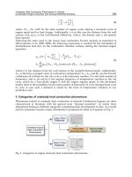
we built a flight model and two engineering models of the PiCPoT satellite shown in Fig. 1.
The satellite has been completely designed using COTS devices, with the only exception
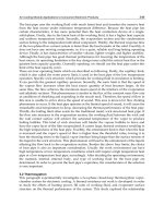
of solar panels. It contains (see Fig. 2): fi ve solar panels; six battery packs; three cameras
219
Use of FRAM Memories in Spacecrafts
8 Will-be-set-by-IN-TECH
Fig. 1. The engineering model of PiCPoT
Solar Panel1
PowerSupply1
Battery6
Solar Panel1
PowerSupply1
PowerSupply1
Solar Panel1
Battery5
PowerSupply1
Solar Panel1
PowerSwitchA PowerSwitchB
Payload
PowerSupply1
Solar Panel1
TxRx 2.4GHzTxRx 437MHz
ProcBProcA
Battery4
Battery3
Battery2
Battery1
Fig. 2. PiCPoT internal structure
with different f ocal lengths; five processors in full redundancy; two RX-TX communication
modules with antennas operating at 437 MHz and 2.4 GHz, respectively; six PCBs, all of them
hosted in a cubic aluminum case, 13cm in side. The radiation behavior of PiCPoT was
carefully considered, because it is a rather complex system containing, as noted, 5 processors,
different kind of memories and programmable logic devices.
In particular we divided the soft errors in the memory devices in three categories:
1. errors on dynamic data and/or in code segments resident in volatile memory;
2. errors on data stored in non-volatile memory;
220
Ferroelectrics - Applications
Use of FRAM Memories in Spacecrafts 9
3. errors on program code stored in non-volatile memory.
The outcome of such events may be wrong data, wrong behavior (if the event affects some
data dependent c ontrol, for instance) or even a crash (i.e., if the upset results in a non-existent
op-code for a processor).
There are several solutions to address this problem, each with its own advantages and
shortcomings. Some cope with all three kind of errors, others do not address all of them.
We applied different techniques in various parts of the satellite, depending on the kind
of protection we wanted to provide. The selection was driven by the need to keep the
design simple and power consumption and total budget low. Therefore we did not use
radiation-hardened devices (too expensive and against the whole philosophy of the project
to use COTS components wherever possible), nor memories with error correcting code (ECC),
useful only for dynamic data and which do not protect against multiple bit upsets.
Even if no radiation-hardened components were used, the susceptibility of COTS components
to radiation can be very different. Careful selection of the best devices for the application
allows us to strongly reduce the probability of single event upsets.
We examined several kind of memories in search for the best ones, and in particular we
considered:
• Dynamic RAM (DRAM): it is t he m ost dense memory and it is used when large amount
of memory is required. It is rather sensitive to radiations. Those parts of the satellite that
depend on this kind of memory must be protected in some way.
• Static RAM (SRAM): it has been shown b y Ziegler et al. (1996) that these are more sensitive
to radiation than dynamic RAMs, but have the advantage of consuming less power.
Processor registers also use the very same technology.
• Flash: Although the charge pump mechanism to reprogram a cell has been shown to be
susceptible to TID ef fects, the cell proved to be robust against S EU, Miyahira & Swift (1998),
because more energy is required to change the state of a bit compared to conventional
RAM devices. For this reason, flash devices are more tolerant to radiation and are a good
candidate for vital data and code.
• Ferroelectric RAM (FeRAM): Compared to flash memories, writing operations on an
FeRAM can operate at lower voltages and are 2 to 3 order of magnitude faster. This allows
saving energy and at the same time maintaining the good tolerance to radiation of flash
devices. This technology looks promising for space applications but few i nformation about
the behavior of FeRAM in space is available in the literature.
We used a mix of al l the above memories because strengths and weaknesses were often
complementary. When available, data on radiation ef fects on memories was used to compare
similar devices and select the best one. Dynamic and static memories were used for execution,
while Flash a nd FeRAM were u sed for permanent data and program storage. Being highly
experimental and having only a few documentation on their behavior, FeRAM was only used
to hold non-vital data, such as the telemetry stream acquired from sensors.
7.2 Operation, timing, fault tolerance
The design of PiCPoT is aimed at high tolerance to faults and radiation effects while using
only COTS components.
The whole design has been based on a redundant architecture we developed mixing both hot
and cold redundancy techniques (Shooman (2001)). Architecture and operation are organized
around a hot-redundant central power management and timing unit, that drives alternatively
221
Use of FRAM Memories in Spacecrafts
10 Will-be-set-by-IN-TECH
two cold-redundant sub-satellites, called processing chain A and B, for housekeeping
measurements (temperature, voltage, current), and a single payload board that co ntrols the
cameras. The two chains are switched on and off alternatively e ach minute to reduce the
effects due to the presence of radiation.
The two sub-satellites have been developed by two different teams, using different
components, in order to avoid the possibility of having the same technological or design issue
on the two systems at the same time. One of the chains has been equipped with a ferroelectric
RAM chip as main storage memory for telemetry data.
7.3 Design constraints
The design and the assembly of a satellite must abide tighter rules than usual “good and
safe design” criteria applied for any electronic system. Moreover, the choice of using COTS
components and technology, allowing failures at the device level, makes mandatory the
adoption of design techniques which guarantee system operation, even in presence of limited
failures.
The design constraints were those already mentioned in Sec. 3.
All mechanical and thermal specifications are easily met by integrated devices. Regarding
cosmic rays, the planned orbit is close to the Van Allen belts, where a limited amount of heavy
ions is present; these radiations may cause latch-up in CMOS devices and single-event upsets
in memories. Due to the low orbit, total dose effects are limited.
As previously discussed, FeRAM devices are able to better cope with all these aspects since:
• T his technology reduces the overall amount of energy required in normal operating mode
with respect to Flash devices, so that the power to be dissipated is a lso reduced, allowing
wider operating temperature conditions and improving the chip behavior in absence of
air.
• The core memory requires lower operative voltages, the electromagnetic emissions are
characterized by less energy and thus they are producing less interference in the satellite.
• The FeRAM cell is less radiation sensitive and thus it improves the overall behavior in
presence of heavy ions.
7.4 Memory requirements
We selected the memory for the various subsystems of our satellite based on the following
considerations.
7.4.1 Size
Knowing the amount of data we have to store is one of the main aspects when selecting a
memory, reducing the number of available technologies and forcing several architectural clues
intheoverallproject(asthethenumberofbitrequiredto addressit,the accessspeed, ).
In our case we had different kind of memory usages and thus different sizes required.
As a first issue we can identify two applications in our project: external memory in PiCPoT
was used for storing telemetry data and for storing images (Passerone et al . (2008)). Obviously
these two usages request different memory sizes and characteristics. Indeed, whilst for
pictures we require a fairly big amount of data (usually some hundreds of kilobytes), for
storing a telemetry history we only need few kilobytes. On the other hand, while loosing a
part of an image can be negligible, or it can be tolerated, loosing telemetry data, thus loosing
information on system behavior, can lead to difficult situations, especially in case of troubles.
Table 1 is resuming these considerations.
222
Ferroelectrics - Applications
Use of FRAM Memories in Spacecrafts 11
Application Memory Size Available Tech. Data loss
Telemetry (1 ÷ 10) kB Flash, EEPROM, FeRAM forbidden
Pictures (0.1 ÷ 1) MB Flash, DRAM, SRAM acceptable
Table 1. Memory size considerations.
7.4.2 Radiation tolerance
At the time we started the development of our satellite, a small number of studies had been
published on the tolerance of commercial FeRAM components to the space environment,
see Nguyen & Scheick (2001) and Scheick et al. (2004). Thanks to these works we were able
to estimate the cross-section for the device chosen in our project. Comparing the cross-section
with the data provided by SPENVIS, we verified the usability of such devices in space.
Figure 3 provides t he output data from the SPENVIS simulation, describing the total radiation
dose for one year of activity. The worst case shielding inside our satellite is about 2 mm of
aluminum.
Concerning TID, the studies mentioned above classified our devices as able to tolerate an
exposure above 10 krad
( Si) and the environmental simulation provided by SPENVIS was
noting only 1 krad
( Si) per year, so we were confident that our project was able to comply
with our orbit without troubles.
At the time we developed our design, there was no direct SEU characterization for the device
we selected, namely a Ramtron 25L256, 256 Kibit with SPI interface.
Therefore we tried to extrapolate the device cross-section considering the above published
data and assuming similar performance from devices built using the same technology.
Simulating the satellite orbit in LEO through SPENVIS we obtained the expected heavy ions
flux, see Fig. 4. By using the estimated cross-section, we obtained in output an average SEU
rate of 0.2 events/day. Moreover, we reduced the actual cross-section by powering off the
device when not used. With a duty-cycle of 10 s/min, we are able to achieve an average SEU
rate of one event per month, thus giving us a good reliability level for our application target
(i.e., minimum mission time of three months).
7.5 Design strategies
Having demonstrated that a FeRAM device can fit our design target, we will now discuss
how to improve, by using architectural solutions, the overall behavior of the memory when
exposed t o the space environment.
7.5.1 Reducing the single event latchup effects
Single event latch-up as exposed in Gray et al. (2001), or simply latch-up (LU), occurs when a
parasitic SCR made by the couple of co mplementary MOS devices is turned on by high input
voltages (this is the usual LU in ICs, caused for instance by input over-voltages) or by high
energy particles which induce a small current (this is the case for a space device). The effect
is a high, self-sustaining current fl ow, which can bring a high power dissipation and, in turn,
device disruption.
LU-free circuits (latch-up cannot occur) can be designed by avoiding CMOS all-together, or by
using radiation hardened technology; since one of the goals of PiCPoT is to explore the use of
COTS components for space applications, we decided to keep only some critical parts LU-free
by proper device selection, and to allow using standard CMOS devices in other circuits. These,
however, must be L U-safe (latch-up can occur, but makes no harm), with specific protection
circuits.
223
Use of FRAM Memories in Spacecrafts
12 Will-be-set-by-IN-TECH
10
−10
10
−5
10
5
10
0
Trapped Protons
Total
Electrons
Bremastrahlung
Dose at Transmission Surface of Al Slab Shields
Dose in Si (rad)
Aluminium Absorber Thickness (mm)
0 5 10 15 20
Fig. 3. Total dose radiation diagram with respect to the shield thickness in LEO orbit.
10
0
10
1
10
2
10
3
10
4
10
5
10
6
10
−10
10
−5
10
0
10
5
10
10
10
−4
10
−2
10
0
10
4
10
2
10
10
10
8
10
6
Spacecraft shield LET spectra
LET (MeV cm^2 g^−1)
Integral Flux (m^−2 sr^−1 s^−1)
Differentiation Flux ((m^−2 sr^−1 s^1) (MeV cm^2 g^−1)^−1)
Fig. 4. Heavy ion flux vs. LET in LEO orbit.
224
Ferroelectrics - Applications
Use of FRAM Memories in Spacecrafts 13
Monostable
CS
IS
Load
CSA
PW
Supply
Fig. 5. Block diagram of latchup protection circuit.
The basic idea behind protection is to constantly measure current and to immediately turn
the power off as s oon as anomalous current consumption is detected. Once the transient
event is over, normal operation can be restored. This technique is analogous to a watchdog
timer, except that it actively mo nitors the circuit to be preserved, rather than waiting for the
expiration of a deadline. Each supply path should have its own protection circuit, which
should itself be LU-free, e.g. using only bipolar technology for its components.
The block diagram of the protection circuit of a single supply path is shown in Fig. 5, and
includes:
• a current sense differential amplifier (CSA),
• a mono-stable circuit with threshold input,
• isolating and current-steering switches (IS and CS),
When the current crosses the limit set for anti-latch-up intervention (usually 2
× the maximum
regular current), the mono-stable is triggered and isolates the load from the power sources for
about 100 ms. To fully extinguish the LU, the shunt switch steers residual current away from
the load.
7.5.2 Reducing the single event upset effects
One technique to approach the problem of SEU effects mitigation is to use redundancy. In
general, at least three replicated units are necessary to implement a voting mechanism, where
the majority wi ns and allows correction of a f ault. The replicated unit can be a complete
board (processor, m emories and peripherals), a physical device on a board (three instances of
the same component) or an abstract unit within a device (three memory segments in the same
chip, holding identical information). This method potentially allows active identification of
an SEU even in RAMs during the execution of a program, and to promptly act to correct
it. However, the space available inside the satellite did not allow us to replicate identical
boards (except for the system level duplications which are discussed in the remainder of this
paper), or even devices within a board. Nonetheless, in some of the processor boards the
program stored in Flash memory is maintained in multiple copies and a procedure to search
for SEUs can be explicitly acti vated. Data, such as p ictures or telemetry, on the other hand,
are not protected and if an SEU occurs, the information downloaded to ground will simply be
incorrect.
Since RAMs, both static and dynamic, including registers inside the processors, are the most
sensitive devices to SEU, and they are not replicated, other techniques must be used to
ensure proper behavior. Our solution is to periodically turn off processor boards and start
a complete boot procedure. Given that the program is stored in flash memory (possibly with
some duplication) and that RAMs go through a power cycle and reset, the soft error will be
225
Use of FRAM Memories in Spacecrafts
14 Will-be-set-by-IN-TECH
completely eliminated. Clearly, data that have to persist for more than one power cycle have
to be stored in some kind of non volatile memory.
Obviously, whatever command was being executed, a SEU will potentially result in wrong
data or a crash. This however does not preclude the system to work correctly at the subsequent
re-boot. The periodicity that was selected is 60s: it allows smooth execution o f all commands
to be executed w ith a good margin. This technique is similar to a watchdog, but the chosen
periodicity is a hard deadline and cannot be extended by the controlled processor boards.
Single event upsets can have different effects depending on the data they are affecting. If
the memory contains raw data coming from sensors used for housekeeping or for simple
monitoring, they a re probably leading only to the invalidation of one o r some of these data:
the overall system behavior is not changed. But, if the memory involved is containing
operating code or parameters used for system configurations, we can have a misbehavior
in the operations executed by our satellite, eventually causing damages. Obviously the latter
are more troublesome and have to be avoided in all the possible ways.
In particular, the FeRAM device contains some functional parameter and not only
housekeeping data, therefore we had to make an extra effort in ensuring the memory tolerance
to the harsh environment. As we exposed earlier in this chapter even if the FeRAM memory
cell can resist to higher cosmic radiation levels than other technologies, the presence of CMOS
elements in the boundary circuitry can cause changes in the stored data (SEFI). The solution
we chose was to reduce the power on time, in order to reduce the time window where the
memory is sensitive to radiation effects and to replicate in three different portions of the device
the functional parameters. Replication of telemetry was not deemed vital and not performed.
7.5.3 Power considerations
PiCPoT is a portable system, even if unconventional. Indeed it is a battery based system and
even if it is also powered by solar panels, it has to survive during the Sun eclipse periods
(about 40 min per 90 min orbit), thus every part of the system should be optimized for power,
as in all the portable devices we deal with everyday.
In Tab. 2 we can see the power budget for each subsystem and in particular for the on-board
processors. This small amount of energy available has to be used effectively in all the
processor boards, i.e., microcontrollers, analog conditioning, and memories.
In our case the external memory is used for two main purposes:
Configuration The OBC can be configured to select different available choices, thus at
the beginning of each power cycle, the processor reads from the outer memory which
configurations have been set and reacts accordingly. Typically these selections are changed
only during the system programming, or by asking from ground to reconfigure the system
in case of damages. Thus, the locations containing such information are mainly read.
Storage of telemetry data W h en we activate the OBC it acquires all the values of all the
sensors available a nd reads all the event counters, in order to build a snapshot of telemetry
data. After completion, telemetry is stored in the external memory, together with running
statistics of all the parameters. These data are read whe n they have to be transmitted to
ground. This usage is more focused on both reading and writing operations.
FeRAM devices have the advantage of b eing more power efficient in writing operations. Since
we are accessing this memory in a balanced way for reading and writing, the usage of FeRAM
devices helped us in reducing the amount of power requiredfor writing operations. Moreover,
being able of completing a writing operation in few tens o f nano seconds, instead o f tens of
milliseconds (as in case of Flash devices), they allow further power saving, since the system
can suspend earlier its operation.
226
Ferroelectrics - Applications
Use of FRAM Memories in Spacecrafts 15
Device Duty Cycle Peak Power Avg Power
PowerSwitch 100% 20 mW 20 mW
Proc A & B 6% 200 mW 12 mW
Payload 0.5% 3.84 W 21 mW
TxRx 2.6% 17.2 W 443 mW
Losses in Batteries & switching 1.07 W
Solar Panels -2.24 W
Margin -674 m W
Table 2. Power budget
7.5.4 Project remarks
Unfortunately we were not able to test this design in space since the launcher blew up during
the launch, causing the destruction of 14 nano-satellites (Malik (2006)). It has been a shame,
since operational data from the design in the environment it has been designed for, would
have produced a great feed-back on our design techniques and solutions. Luckily the grown
experience has been reused in the new project we are working on, that is described in the next
section.
7.6 A modular architecture for nano-satellites
Thanks to the experience got by the design of PiCPoT we decided to use again FeRAM devices
in our new spaceborne project, called AraMiS, p r esented in Speretta et al. (2007). The aim of
this project is to design, prototype and develop a new architecture for modular small satellites.
The most effective way to reduce the cost of a nano- or micro-satellite mission is to reduce as
much as possible design and non-recurrent fabrication costs, which usually account for more
than 90% of the overall budget. Reducing them can be achieved only by sharing the design
among a large number of missions.
Design reuse is the rationale behind the AraMiS project, that is to have a modular architecture
based on a small number of flexible and powerful modules which can be reused as much as
possible in different missions. Using the same module(s)more times obviously allows to share
design, qualification and testing costs and to reduce the time-to-launch.
The first step in the AraMiS project has been to identify the most common and critical
subsystems. We have then concentrated our efforts on the following subsystems, which are
described in details in Speretta et al. (2007) and in Speretta et al. (2009):
1. m echanical subsystem;
2. p ower management subsystem;
3. telecommunication subsystem;
4. on-board processing subsystem;
5. payload support.
The basic architecture of AraMiS is based on one or more modular intelligent tiles.Mostof
them are to be regularlyplaced on the outer surface of the satellite and have a double function:
mechanical and functional. The inner part of the satellite is mostly left empty (except for the
on-board processor and payload support tile), to be filled by the user-defined payload, which
is the only part to be designed and manufactured ad-hoc for each mission.
The power management subsystem a ims at managing all the aspects r elated to energy, i.e.,
collecting energy from solar cells, storing it on the available batteries, and guaranteeing their
correct discharge when modules requires energy to operate. The telecommunication subsystem
227
Use of FRAM Memories in Spacecrafts
16 Will-be-set-by-IN-TECH
contains the modems, the transceivers, the radio-frequency components, and the antennas
used to communicate with the ground stations. The on-board processing subsystem contains
the main processors and units devoted to the computation and the high speed communication
among the tiles and the modems. A t last, the payload subsystem is the only part not designed
at the moment, since it can vary from mission to mission, thus we only developed the
communication and the mechanical interfaces.
Each tile is designed, manufactured and tested in relatively large quantities. Reuse also allows
to put an increased design effort to compensate for the lower reliability of COTS devices,
therefore achieving a reasonable system reliability at a reduced cost.
7.6.1 Modularity and customization
The aim of our design is to study, develop, and produce a structure, a set of tiles, and a set of
interfaces to allow universities and small enterprise to access the space in a easy and affordable
way.
Thus the concept of modularity in all part of our design has to be the leit motif.Modularity
means a set of re dundant functions and resources that can be configured and used when
needed (both during the pre-launch phase and at run-time). Many of these features have to be
changed easily, thus using a configuration memory is the straightforward choice. The number
of available selections is pretty limited (i.e., can vary from 10 to hundred in the projects we
have foreseen), but they have to be maintained for all the satellite life. For this reasons FeRAM
devices are the most suitable to this goal.
7.6.2 Operational conditions
The target environment for our design is again the low-earth orbit, a zone between the 500 km
and the 800 km above the sea level. The environment is the same of the PiCPoT satellite we
described above, thus the related constraints are the same.
7.6.3 OBC-tile architecture
The OBC-tile architecture is shown in Fig. 6. It is based on a hot redundancy structure relying
on FPGAs and CPUs. This OBC relies on the presence of an MSP430 (TI (2010)) microcontroller
and an Actel FPGA A3P125. The former is used for handling basic operation of the tile, like
thecommunicationthroughthecontrolbus,sensorsacquisition,JTAGinterface Thelatter is
aimed at performing all the data crunching related to the image elaboration and the high speed
communication with the payload and the radio subsystem.
In order to save power the FPGA i s switched on only when needed and the MSP430 is enrolled
to manage the power cycling of this device.
Since this module has to be able to work in different cases (e.g., different power cycles,
different hardware configurations, differentpayloads, ) we need to keeptraceofallthese
choices somewhere. Obviously a memory is a good place to keep it, but due to our power
constraints, we need to shut the memory down when it is not accessed. Thus the usage of
a non-volatile technology is mandatory and, how we exposed before for the PiCPoT case,
FeRAMs is the best choice.
In our case we use multiple smaller chips, even if greater ones are commercially available, for
reliability reasons, since in case of physical damages we can have multiple places where to
save our configuration data. Moreover having multiple chips allows us to save more energy
since we power only the device needed, and not all the memory we have on board.
228
Ferroelectrics - Applications
Use of FRAM Memories in Spacecrafts 17
Fig. 6. AraMiS OBC architecture
8. Conclusions
This chapter has shown how commercial-off-the-shelf FeRAM devices can be a good solution
for spacecrafts. I ndeed we described how the FeRAM memory cell is far less sensitive to the
issues we can have in space (i.e., heavy ions and total ionizing dose). Moreover its intrinsic
low power consumption allow the devices to be very w ell suited for battery-based devices
and those applications where heat dissipation is difficult.
After this introduction two real designs have been presented, where the usage of FeRAM
memories has produced a set of non negligible improvements. F urther investigations are
ongoing and we plan to use again these devices in our future projects, in order to make our
designs safer and more reliable.
Unfortunately we did not collect data from the PiCPoT experiment, since itblew up during the
launch due to a failure of the launcher. But the new project will provide us a lot of information
from the real application field allowing us to increase our expertise in using these kind of
devices in the space and will allow our future designs to be more reliable, robust, and efficient.
9. References
Benedetto, J., Derbenwick, G. & Cuchiaro, J. (1999). Single event upset immunity of
strontium bismuth tantalate ferroelectric memories, Nuclear Science, IEEE Transactions
on 46(6): 1421 –1426.
Gray, P. R., Hurst, P. J., Lewis, S. H. & Meyer, R. G. (2001). Analysis and Design of Analog
Integrated Circuits,JohnWiley&Sons,Inc.
Kamp, D., DeVilbiss, A., Haag, G., Russell, K. & Derbenwick, G. ( 2005). High density radiation
hardened ferams on a 130 nm cmos/fram process, Non-Volatile Memory Technology
Symposium, 2005, pp. 4 pp. –51.
229
Use of FRAM Memories in Spacecrafts
18 Will-be-set-by-IN-TECH
Malik, T. (2006). Report: Dnepr rocket crashes shortly after launch.
URL: />Miyahira, T. & Swift, G. (1998). Evaluation of radiation effects in flash memories, Proceedings
of the Military and Aerospace Applications of Programmable Devices and Te chnologies
Conference.
NASA-Gsfc (2000). Single Event Effects.
URL: />Nguyen, D. N. & Scheick, L. Z. (2001). TID testing of ferroelectric nonvolatile RAM, Proceedings
of the Radiation Effects Data Workshop, Vancouver, BC, Canada, pp. 57–61.
Passerone, C., Tranchero, M., Sp eretta, S., Reyneri, L. M., Sansoè, C. & Del Corso, D. (2008).
Design solutions for a university nano-satellite, Proceedings of the Aeroconf.
Philpy, S., Kamp, D. & Derbenwick, G. (2003). Hardened by design ferroelectric memories for
space applications, Non-Volatile Memory Technology Symposium, 2003, p. 4 pp.
Scheick, L., Guertin, S. & Nguyen, D. (2004). SEU evaluation of FeRAM memories for space
applications.
URL: />scheick_p.pdf
Sheikholeslami, A. & Gulak, P. (2000). A survey of circuit innovations in ferroelectric
random-access memories, Proceedings of the IEEE 88(5): 667 –689.
Shiga, H., Takashima, D., Shiratake, S., Hoya, K., Miyakawa, T., Ogiwara, R ., Fukuda, R.,
Takizawa, R., Hatsuda, K., Matsuoka, F., Nagadomi, Y., Hashimoto, D., Nishimura,
H., Hioka, T., Doumae, S., Shimizu, S., Kawano, M., Taguchi, T., Watanabe, Y.,
Fujii,S.,Ozaki,T.,Kanaya,H.,Kumura,Y.,Shimojo,Y.,Yamada,Y.,Minami,Y.,
Shuto, S., Ya makawa, K., Yamazaki, S., Kunishima, I., Hamamoto, T., Nitayama, A.
& Furuyama, T. (2010). A 1.6 gb/s ddr2 128 mb chain feram with scalable octal bitline
and sensing schemes, Solid-State Circuits, IEEE Journal of 45(1): 142 –152.
Shooman, M. (2001). Reliability of Computer Systems and Networks,JohnWiley&Sons,Inc.
SPENVIS (n.d.). SPENVIS, the Space Environment Information System.
URL: />Speretta, S., Reyneri, L. M., Sansoè, C., Tranchero, M., Passerone, C. & Del Corso, D.
(2009). Optical-based cots data communication bus for satellites, Acta Astronautica
66: 674–681.
Speretta, S., Reyneri, L., Sansoè, C., Tranchero, M., Passerone, C. & Del Corso, D. (2007).
Modular architecture for satellites, Proceedings of 58
th
International Astronautical
Congress, Hyderabad, India.
TI (2010). MSP430 Family User’s Guide.
Ziegler, J. F., Curtis, H. W., Muhlfeld, H. P., Montrose, C. J., Chin, B., Nicewicz, M., Russell,
C.A.,Wang,W.Y.,Freeman,L.B.,Hosier,P.,LaFave,L.E.,Walsh,J.L.,Orro,J.M.,
Unger, G. J., Ross, J. M., O’Gorman, T. J., Messina, B., Sullivan, T. D., Sykes, A. J.,
Yourke, H., Enger, T. A., Tolat, V., Scott, T. S., Taber, A. H., Sussman, R. J., Klein, W. A.
& Wahausand, C. W. (1996). Ibm experiments in soft fails in computer electronics,
IBM Journal of Research and Development 40(1).
230
Ferroelectrics - Applications
0
Adaptive Boolean Logic Using Ferroelectrics
Capacitors as Basic Units of Artificial Neurons
Alan P. O. da Silva
1
, Cicília R. M. Leite
2
, Ana M. G. Guerreiro
3
, Carlos A. Paz
de Araujo
4
and Larry McMillan
5
1,3
Federal University of Rio Grande do Norte
2
State University of Rio Grande do Norte And College of Science and Technology Mater
Christi
4,5
Symetrix Corporation
1,2,3
Brazil
4,5
USA
1. Introduction
Neural networks are being investigated as a computational paradigm in many fields of
artificial intelligence.
The pioneers of cybernetics were clearly inspired by neurology and the current knowledge
of the human brain to develop the architectures of modern computing machines. The
evolution has given the brain very distinctive capabilities of learning, distributed memory,
computation, generalization, robustness, and the capability of interpretation of imprecise and
noisy information, etc., not present in Von Neumann computers.
Neuroengineers have come up with the idea of using Artificial Neural Networks (ANNs)
massively parallel computing machines inspired by the biological nervous systems. However,
ANNs have a very different approach and computing paradigm, where learning from
examples and learning from iteration replaces our common idea of programming. These
models achieve good performance via massively parallel networks composed of generally
nonlinear computational elements, referred to artificial neurons. Synaptic weights are
associated with each neuron connection between neurons. In the case of classical ANNs, the
activation potential and the synaptic weights are analogous, respectively, to the firing rates
and the strength of the synapse in biological neurons which are arranged in layers.
The first, very simplified model, mathematical model of a neuron operating in an all-or-none
fashion: the Threshold Logic Gate (TLG). It did not take very long for a hardware
implementation to be developed. Since then a lot of researh have been developed with the aim
of implementing artificial neurons in hardware and construct intelligent systems On-Chip.
Many theoretical results have been shown that threshold logic circuits are more powerful
and/or efficient than Boolean circuits (Beiu et al., 2006). Exploiting the principle for electronics
circuits may reduce the number of transistors and interconnections (Shibata and Ohmi, 1991).
Output-wired threshold gates working in the classical above threshold domain have been
implemented, too. A lot of work has been done in this area. Thinking on this scenario, this
chapter shows a implementation of the boolean logic with artificial neuron type model with a
11
2 Will-be-set-by-IN-TECH
Ferroelectric (Fe) capacitor as its basic unit. The Fe Capacitors was chosen because it have been
embedded into LSIs as Ferroelectric Random Access Memory (FeRAM) and their reliability
data have been accumulated. The capacitors are high impedance device, and it is an advantage
for low power consumption, besides the configuration can be changed after packaging. The
FeCapacitor uses the phenomenon of the hysteresis loop as the activation function for the
neuron model. The model performs a weighted sum of the inputs and applies it the non-linear
activation function generated by a single side of the hysteresis. Changing the weights, it is
possible to reconfigure the gate easily. Ones tries to show a new way of implementing a
neuron, without using transistors.
We developed the perceptron model with the FeCapacitor, that we called here FePerceptron,
and we also developed the FeSpiking Neuron model, that is an extended model for the
spiking neuron (Guerreiro et al., 2008) using the FeCapacitor as its basic unit for the activation
function. Both models is going to be simulated and tested in Matlab. The models were used to
simulated all logical gates and synthesis of several digital circuits as D-flip-flop, shif-register,
full adders, and a simple CPU with the Spiking FeNeuron. The Spiking FeNeuron is
developed because it can simulated all logical gates, inclusive the XOR gate with single
neuron, which is impossible with a single Perceptron.
Because of the simplicity, we started the hardware implementation with the FePerceptron in
an Field Programmable Gate Arrays (FPGA). The FeCapacitor is developed as its basic unit
and can be used in any neuron model as activation function. We used the DSP builder of
Altera to generate the model. The DSP Builder Signal Compiler block reads Simulink Model
Files developed (.mdl) that are built using DSP Builder blocks and generates the VHDL files.
This is the first step of a work to implement in hardware the neuron using FPGAs simulating
the desired hardware, bringing a second degree of reconfigurability to the FPGAs with the
adaptive boolean logic CPU.
This chapter is organized as follow, first in section 2 we give an overview of several developed
works and researches that were done simulating and implementing neural networks in
hardware. Section 3 shows the development of the mathematical model of the FeCapacitor.
The FeCapacitor model is used as activation function to the Perceptron model generating the
FePerceptron and to the Extended Spiking Neuron model generating the FeSpiking Neuron
Model as shown in section 4. The simulations in Matlab of both models are shown in section
5 with the realization of boolean logic gates and adaptive boolean circuits. The section 6 is
responsible to shown the FePerceptron model developed in an FPGA. Finally, conclusion are
presented in section 7.
2. History of neuron models, simulations and implementation of neural networks
in hardware
The hardware implementations means and introduces for example computational errors,
degradation of learning and lack of accuracy in results. This are some issues that have been
studied and address and explored in many researches. These include digital (Bermak and
Martinez, 2003; Kung, 1992; Lenne, 1995), analog (Brown et al., 2004; Mead, 1989), hybrid
(Lehman et al., 1996; Schmid et al., 2004), FPGA based (Nedjah and Mourelle, 2007; Rak
et al., 2009; Schrauwen and D’Haene, 2005), and (non-electronic) optical implementations
(Moerland, 2007; Tokes et al., 2000).
In spite of all the difficults to implement ANN in hardware a lot of research have been done.
There is a lot of needs in real-world applications. Some examples are: optical character
recognition, robotics, voice recognition, adaptive filters, image analysis, finger print feature
232
Ferroelectrics - Applications
Adaptive Boolean Logic Using Ferroelectrics Capacitors as Basic Units of Artificial Neurons 3
extration, acoustic sound recognition, olfactory sensing, traffic monitoring, experiments in
high energy physics (Lamela and Ruiz-Llata, 2005), and adaptive control.
There are indeed several surveys which have appeared in the past. There is this one (Janardan
and Indranil, 2010) that has done a survey which includes most of all works concerning
Hardware Neural Networks (HNN). Here, we only give a small overview over what was
done in the past based on (Janardan and Indranil, 2010), so the importance of the HNN
can be noticed, and seen that a lot of research has already been developed. Some early
references on the VLSI implementations can be found on (Mead, 1989) and (Glesner and
Poechmueller, 1994). An overview on neurocomputers up to the 90’s, built from accelators
boards, general purpose hardware, and neurochips can be found on (Heemskerk, 1995).
Digital implementations with custom processors can be found (Ienne, 1996).
Sundararajan and Saratchandran (1998) discuss in detail various parallel implementation
aspects of several ANN models using various hardware architectures. Zhu and Sutton
(2005) survey FPGA based implementations of ANNs discussing different implementation
techniques and design issues. Smith also discuss and survey digital and analog VLSI
implementations approaches in neural model.
One of the latest surveys with specific focus to commercially available hardware can be
found on Dias et al. (2004). Neurofuzzy hardware systems is discussed concerning aspects
of various tecnologies of hardware implementations and software co-design techniques.
Implementations of Spiking Neural Networks is provided by (Schrauwen and D’Haene, 2005).
Valle (2005) presents various approaches to built smart adaptive devices.
There still some topics as hardware friendly learning algorithms, as pertubation learning
(Jabri and Flower, 1991), constructive learning (Smieja, 1993), cascade error projection learning
(Duong, 1995; Duong and Stubberud, 1995), and local learning (Chen et al., 2000). Some
HNN based on Multilayer Perceptron (MLP) (D’Acierno, 2000; Kumar et al., 1994), radial
basis function (Fakhraie et al., 1994; Verleysen et al., 1994; Yang and Paindavoine, 2005), and
Neocognition (Patnaik and Rao, 2000) and neurocomputers(Glesner and Poechmueller, 1994;
Strey and Avellana, 2000).
3. The mathematical model of ferroelectrics capacitor
There are two areas of research to be investigate, the physically based models and the
behavioral models. In our work, the bahavioral modeling was chosen because it does not
required a detailed knowledge of ferroelectric theory; it only requires a careful observation of
the ferroelectric capacitor behavior from the circuit point of view.
A lot of research have been done in attempts to models the behavior of a ferroelectric
capacitors (for a review, see: (Sheikholeslami and Gulak, 1997) since they were introduced
as storage elements in integrated nonvolatile memory applications.
In this paper, the Mathematical Model (Miller et al., 1991) is used that introduces a closed form
mathematical equation for the hysteresis loop.
Based on the saturability of the switching polarization and the symmetry of the hysteresis
loop, the mathematical model approximates the saturated polarization loop with two
hyperbolic functions:
P
+
sat
(E)=P
s
tanh[
E − E
c
2δ
] (1)
and,
233
Adaptive Boolean Logic Using Ferroelectrics Capacitors as Basic Units of Artificial Neurons
4 Will-be-set-by-IN-TECH
P
−
sat
(E)=−P
+
sat
(−E) (2)
where P
+
sat
(E) and P
−
sat
(E) represent the polarization corresponding to the positive and
negative going branches of the hysteresis loop, respectively. P
s
and E
c
are the saturation
polarization and the coercive field extracted from an actual hysteresis loop. With the fixed
P
s
and E
c
, δ is uniquely specified by P
r
, the remanent polarization, through the following
equation:
δ
= E
c
[ln(
1 + P
r
/P
s
1 − P
r
/P
s
)]
−1
(3)
A sketch of the hysteresis loop is done with MATLAB as it is shown in Figure 1. The symmetry
with respect to the origin in this Figure is guaranteed by Equation (2).
Pr
-Pr
Ps
-Ps
Ec
Fig. 1. The hyperbolic tangent functions approximate the Saturated Polarization Loop. The
hysteresis loop is plotted considering the values of P
s
=23μ C/cm
2
, P
r
=15μ C/cm
2
,andE
c
= 40kV/cm
2
borrowed from an actual saturated hysteresis loop.
The Mathematical Model provides a good approach for steady-state analysis of ferroelectric
capacitor behavior, and this model is sufficient by now for this work. Future simulations
maybe can incorporate the transient analysis and by than mode accurate models can be
necessary.
4. The ferroelectrics capacitor as an activation function of artificial neurons
4.1 Perceptron model
The biological neuron is the structure unit of the nervous systems. It considers of a cell body,
called soma, axon and several ramifications. These ramifications are called, dendrites. The
dendrites conduct action potentials or electrical pulses toward the body cell and conform in
large and complicated trees. The dendrites and the soma constitute the input surface of the
neuron. The axon consists of a large fiber whose branches form the axonal tree. The axon has
a arborization at its terminal. The tips of the branches of the axon are called nerve terminals,
boutons or synaptic knobs. The axon acts as a transmission line. The action potential travels
along an axonal tree all the way to the nerve terminals. The terminals of the branches make
contacts with the dendrites of other neurons. The contacts are called synapses.
234
Ferroelectrics - Applications
Adaptive Boolean Logic Using Ferroelectrics Capacitors as Basic Units of Artificial Neurons 5
The first computational model of the biological neuron was introduced by McCulloch and
Pitts (McCulloch and Pitts, 1943) in the 1940s. McCulloch and Pitts merged mathematical
logic and neurophysiology to propose a binary threshold unit as a computational model for
an artificial neuron operating in discrete time. The output y
k
(t)ofaneuronis1whenanaction
potential is generated, and
−1 otherwise. A neuron fires when the effects of inhibitions and
excitations are larger than a certain threshold, θ.
In 1958, the American psychologist Rosenblatt proposed a computational model of neurons
that he called The Perceptron (Rosemblatt, 1958). The essential innovation was the introduction
of numerical interconnection weights.
A neuron is an information processing unit that is fundamental to the operation of a neural
network (Haykin, 1998). The perceptron model of the neuron has three basic elements (Figure
2):
1. Synapses that are characterized by the strength of the weights;
2. An adder for summing the input signals, weighted by the respective synapses and the
threshold of the neuron;
3. An activation function for limiting the amplitude of the output (in this case completely
unclocked with the firing event).
Fig. 2. Perceptron Model
The external threshold, denoted by θ, has the effect of increasing or lowering the net input of
the activation function, depending on whether it is positive or negative.
The perceptron consists of a linear combiner followed by a non-linear function, as depicted
in Figure 2. The summing node of the neuronal model computes a linear combination of
the inputs, x
i
, applied to the synapses connections, w
i
, and also incorporates an external
threshold, θ. The resulting sum, that is, the induced local field, is applied the activation
function. The activation function denoted by Φ
(υ), defines the output of the neuron in terms
of the local field, υ. The activation function usually used is a sigmoid. The weights model the
synaptic strength, and the output of the neuron models the rate of fire of biological neurons.
The threshold can be accounted for in two ways: adding a new input signal fixed at
+1or
adding the threshold to the linear combination of the input with the weights.
The neuron can be described mathematically as:
υ
=
p
∑
j=1
ω
j
x
j
(4)
235
Adaptive Boolean Logic Using Ferroelectrics Capacitors as Basic Units of Artificial Neurons
6 Will-be-set-by-IN-TECH
and
y
= φ(υ + ω
0
θ) (5)
The capacity of learning is one of the most important characteristics of an ANN. Learning
is closely related to an improvement of performance of the system. This is achieved by
minimizing errors, self-organizing information through correlations of data, and maximizing
rewards in a trial-and-error system over time. In practice, learning is achieved by adjustment
of the free parameters of the ANN.
4.1.1 The FePerceptron model
Our simplified model is based on the perceptron model, using the following concepts: inputs,
synapses strength, adder, activation function and the threshold.
The FeNeuron uses the ferroelectric capacitor as its basic unit. The model (Figure 3) is
composed by the input, x
i
, by the synaptic weights, w
i
, as resistors, combining them linearly.
The result is applied to the ferroelectric capacitor performing the output of the model. The
phenomenon of the hysteresis loop is used to act as the activation function. It is necessary to
use only one side of the hysteresis loop.
Fig. 3. The FeNeuron Model
The induced local field of the neuron is computed as in Equation (4). The output is described
as:
y
= P
+
sat
(υ + ω
0
θ) (6)
and,
P
+
sat
= P
+
sat
/P
s
(7)
The Equation (6) can be re-written as:
y
= P
+
sat
(
p
∑
j=1
ω
j
x
j
+ θ) (8)
The goal of the model in this case is to classify correctly the set of externally applied stimuli,
x
1
, x
2
, x
3
, , x
p
into two classes. In our work, we are treating with Boolean functions with
236
Ferroelectrics - Applications
Adaptive Boolean Logic Using Ferroelectrics Capacitors as Basic Units of Artificial Neurons 7
two inputs, thus our network is a single layer, with only one neuron with two inputs plus the
threshold and one output.
4.2 Extended Spiking Neuron model
Artificial spiking neurons are biophysical models which try to account for properties of
biological neurons by modeling the integrated signal flow through parts of the neuron. The
input spike signals, from presynaptic biological neurons are weighted, summed up and
passed through a type of leaky integrator. If the membrane potential exceeds a certain
threshold, a spike is generated. The pulses arrive at the input synapses in discrete time. The
Extended Spiking FeNeuron is a discrete model composed of an input layer, synaps weights,
first order recursive filters, a soma, a hard limiter and the membrane potential. The input layer
receives the input spikes. The weights are the synaptic strength values. The soma provides
a linear combination of the input signal passing through the first order recursive filters and
summing with the thresholds coming from the feedback loop. The hard limiter compares the
soma potential with the threshold and emits a spike depending on the soma threshold.
The membrane potential is responsible to compute the delay necessary for the neuron to
compute. The delay is build up by the summing potential of the input signals and depends
on the time delay of the filters and more important on the delay caused by the feedback loop
where the dynamic threshold sets the time of firing. We can define a neuron i that receives
inputs from presynaptic neurons j
∈ Γ
j
,where
Γ
i
= {j/j presynaptic to i } (9)
The discrete model considers a "1" for a incoming spike and "0" for the absence of a spike. The
input passes through the first order recursive filters and then is summed up. The Equation 10
describes the action of the first order recursive filters:
u
fij
= e
−(T/τ
ij
)
u
fij
(n − 1)+ω
ij
(n)x
ij
(n) (10)
where x
ij
(n) is the input of the synapses, w
ij
(n) is the synapses weight, T
ij
is a constant delay
of the filter, u
fij
(n) is the output of the first order recursive filter in a time slice, n.
The dynamic threshold is describe by the following equation:
θ
(n)=ϑ + θ
1
(n) (11)
θ
1
(n)=p
i
(n)r
i
(n) (12)
where ϑ is the static threshold and pi
(n) is the output of the first order recursive filter of the
feedback loop.
The r(n) is defined as:
r
i
(n)=ξ(|p
i
(n)|−
q
∑
j=1
x
ij
(n)) (13)
where q is the length of the input vector.
The function ξ
(.) is defined as:
ξ
(υ)=1/2 + 1/2(er f (υ/(2k))) (14)
This function is implemented by the Ferroelectric Capacitor.
237
Adaptive Boolean Logic Using Ferroelectrics Capacitors as Basic Units of Artificial Neurons
8 Will-be-set-by-IN-TECH
The equation of the first order recursive filter of the feedback loop is:
p
i
(n)=ap
i
(n − 1)+g
i
(n) (15)
where g
i
(n) is the output dependent on y
i
(n) and r
i
(n)
g
i
(n)=ξ(r
i
(n) − y
i
(n)) (16)
The state mp
i
(n) of the model neuron i can be rewritten as:
mp
i
(n)=−{υ + p
i
(n)r
i
(n)} +
∑
j∈τ
(ω
ij
(n)u
fij
(n)) (17)
The output y
i
(n):
y
i
(n)=ξ(mp
i
(n)) (18)
The process of accumulation voltage and transformation to time is described by the block
diagram named as membrane potential in Figure 4. From the figure we notice that θ
1
(n)
depends on the feedback of the output and on the input signals. The filter of the feedback loop
is a first order recursive filter with the coeficient equal to a. The absolute value of the filter
output
(pi(n)) subtracts from the sum of the inputs. Until the filter output reaches the sum
of the inputs, the feedback loop accumulates voltage. This is done, by passing the response
of
|p
i
(n) −
∑
q
j
=1
x
ij
(n)| through the ξ(υ) function (Eq. 7), resulting in r
i
(n).Theξ(υ) function
is implemented by hystheresis of the FeCapacitor. The result of r
i
(n) is equal to 1 when the
output of the filter is equal or greater to the sum of the input signal, and 0 otherwise. The
r
i
(n) is multiplied by (p
i
(n)) resulting in the dynamic threshold that is the response of the
membrane po- tential block diagram. The dynamic threshold accumulates charge until a spike
occurs and the filters are reset. Our work has mapped the biological behavior of accumulating
charge to create the receptor field by adding the membrane potential block diagram described
in Figure 4 to the spiking neuron model. Using this approach it is possible to solve non-linear
problems (XOR - problem) with a single neuron with the hard limiter function as activation
function
(ξ(υ)).
5. The simulations of the models in simulink by Matlab
5.1 FePerceptron model
The results show the the simulation of the FeNeuron performing the logic gates, AND,
OR, NAND and NOR. The model performs thresholding operations with a very simple
architecture. It was developed in MATLAB environment.
The simulated gates have an architecture of a single neuron. The synaptic weights, ω
1
and ω
2
of the model were adapted iteration-by-iteration basis. For the adaptation process, the neuron
was trained with the error-correction rule as a convergence algorithm. This algorithm uses
a supervised paradigm which means that the desired response is presented in the training
process. The desired response is the output of the logic gate that has been simulated with the
respective input, following the well-known truth table of logic gates.
The algorithm can be described as follow:
Variables and Parameters:
The inputs: x
(n)=[θ x
1
x
2
]
T
The weights: w(n)=[ω
0
ω
1
ω
2
]
T
238
Ferroelectrics - Applications
Adaptive Boolean Logic Using Ferroelectrics Capacitors as Basic Units of Artificial Neurons 9
Fig. 4. The Discrete Spiking FeNeuron Model
The actual response: y
(n)
The desired response: d(n)
The learning rate, or a positive constant less than a unit: η
The mean square error: error
(n)
1. Initialization: Randomize w( n). Perform the computations from n = 0, 1, 2, until the
mean square error is minimum.
2. Computation of the actual response with (18).
3. Adaptation Process:
w
(n + 1)=w(n)+η[e(n)]x(n) (19)
e
(n)=d(n) − y(n) (20)
error
(n)=
1
2
∑
j∈Γ
e
2
(n) (21)
where Γ includes all neurons in the output layer of the network. In our case, only a single
neuron is used.
4. Increment time step n by one and goes back to 2.
After the training process, the weights were computed and can be used to simulate the logic
gates. The learning curves are shown in Figure 5 with the computed parameters.
The model performs thresholding operations with a very simple architecture. The Boolean
functions performed by the model is soft programmable. This is accomplished by only
adjusting the weight values of the synaptic connections. It is a very simple model that
was easily implemented by software and can be extended to hardware implementations. As
hardware implementations, this model brings the contribution of being very simple and can
perform several functions with only changing the free parameters of the structure that can be
soft-programmable.
239
Adaptive Boolean Logic Using Ferroelectrics Capacitors as Basic Units of Artificial Neurons
10 Will-be-set-by-IN-TECH
Mean Square Error
Iterations
AND GATE
Weights = [ -0.3759 0.6389 0.6389 ]
Actual Output = [ -0.0006 0.0015 0.0015 0.9981 ]
Desired Output = [0001]
Minimum error = 0.0000059874
Mean Square Error
Iterations
NAND GATE
Weights = [ 1.5709 -0.6503 -0.6503 ]
Actual Output = [ 1.0000 0.9988 0.9988 0.0017 ]
Desired Output = [1110]
Minimum error = 0.0000059874
Mean Square Error
Iterations
OR GATE
Weights = [ 0.2528 0.7089 0.7089 ]
Actual Output = [ 0.0013 0.9995 0.9995 1.0000 ]
Desired Output = [0111]
Minimum error = 0.0000020539
Mean Square Error
Iterations
NOR GATE
Weights = [ 0.9145 -0.6688 -0.6688 ]
Actual Output = [ 0.9986 0.0011 0.0011 -0.0009 ]
Desired Output = [1000]
Minimum error = 0.0000052702
Fig. 5. The learning curves with the parameters for each computed logic gate. The inputs
were (0 0), (0 1), (1 0) and (1 1). The threshold was considered equal to +1 for all gates.
240
Ferroelectrics - Applications
Adaptive Boolean Logic Using Ferroelectrics Capacitors as Basic Units of Artificial Neurons 11
5.2 Spiking FeNeuron model
In a digital simulation, the time period, n, is called a time slice. The four major steps of
computing are:
1. Input phase: The input of each synaptic dendrite connection multiplied with the respective
synaptic weight.
α
ij
(n)=ω
ij
(n)x
ij
(n) (22)
2. Filter phase: The signals from the input phase pass through the recursive filters.
ufij
(n)=α
ij
(n)+e
−
T
τ
ij
u
fij
(n) (23)
3. Output phase: The sum of the signals from the filter phase are summed to produce the
membrane potential. If the membrane potential exceeds the dynamical threshold, an output
spike is generated.
The state mp
i
(n) of the model neuron i can be rewritten as:
mp
i
(n)=−{υ + p
i
(n)r
i
(n)} +
∑
j∈τ
(ω
ij
(n)u
fij
(n)) (24)
p
i
(n)=ap
i
(n − 1)+g
i
(n) (25)
g
i
(n)=ξ(r
i
(n) − y
i
(n)) (26)
y
i
(n)=ξ(mp
i
(n)) (27)
ξ
(υ)=
1
2
+
1
2
er f
(
υ
2k
) (28)
If the spike is generated, the filters are reset. Otherwise the filter still accumu- lates potential.
4. Learning phase: The synaptic weights are adjusted with the Steepest Descent method.
ω
ij
(n + 1)=ω
ij
(n)+γ( d
i
(n) − y
i
(n)) x
ij
(n) (29)
where d
i
(n) is the desired output, y
i
(n) is the actual output, x
ij
(n) is the input, and γ is the
learning rate.
These computation steps will be used in the logical functions problems. The computation of
Boolean functions is a classification problem and as such it consists of separating the data into
classes based on a discriminant function. There are two classes (0 or 1), and the input space is
composed of four entries, each one with length two, except for the NOT logical gate that has
one input and one output that negates the input.
Figure 6 (a) shows the learning curve for all logical gates and Figure 6 (b) shows for the
XOR. The training phase is the same for all Boolean functions, we just have to modify the
desired output to suit each logical gate. The weights and the filter coeficient are summarized
in table I. The learning rate used was 0.01 and the filter coeficients of the first order recursive
filter (τ
ij
) were 0.01. Depending on the learning rate and the initial values of the weights the
convergence rate changes.
Figure 7 shows the new symbol adopted for the neural logical gates and the output vector after
the training process. The result is a perfect truth table of the respective logical gates. Table 1
shows the values for the decay constants, the weights and the learning rates for each logical
241
Adaptive Boolean Logic Using Ferroelectrics Capacitors as Basic Units of Artificial Neurons