Flash Memories Part 4 pot
Bạn đang xem bản rút gọn của tài liệu. Xem và tải ngay bản đầy đủ của tài liệu tại đây (828.82 KB, 20 trang )
Error Control Coding for Flash Memory 19
Fig. 8. Example of Tanner graph.
5. Low-Density Parity-Check (LDPC) code
LDPC code is a linear block code defined by a sparse parity-check matrix (Gallager, 1962), that
is, t he number of non-zero element in an m
×n parity-check matrix is O(n). The LDPC codes
are employed in recent high-speed communication systems because appropriately designed
LDPC codes have high error correction capability. The LDPC codes will be applicable to
high-density MLC flash memory suffering from high BER.
5.1 Tanner graph
An LDPC matrix H =[h
i,j
]
m×n
is expressed by a Tanner graph, which is a bipartite graph
G =(V, E),whereV = V ∪ C is a set of nodes, and E is a set of edges. Here, V = {v
0
, v
1
, ,
v
n−1
} is a set of variable-nodes (v-nodes) corresponding to column vectors of H,andC =
{
c
0
, c
1
, ,c
m−1
} is a set of check-nodes (c-nodes) corresponding to row vectors of H.The
edge set is defined as
E = {(c
i
, v
j
)|h
i,j
= 0}. That is, c-node c
i
and v-node v
j
are connected by
an e dge
(c
i
, v
j
) if and only if h
i,j
= 0. Girth of G is defined as the length of shortest cycle in G.
The girth affects the error correction capability of LDPC code, that is, a code with a small girth
l, e.g., l
= 4, will have poor error correction capability compared to codes with a large girth.
Example 21. Figure 8 presents a parity-check matrix H and corresponding Tanner graph
G.
5.2 Regular/irregular LDPC code
5.2.1 Regular LDPC code
Regular LDPC code is defined by a parity-check matrix whose columns have a constant
weight λ
m and rows have almost constant weight. More precisely, Hamming weight
w
c
(H
∗,j
) of the j-th column in H s atisfies w
c
(H
∗,j
)=λ for 0 ≤ j ≤ n − 1, and Hamming
weight w
r
(H
i,∗
) of the i-th row in H satisfies nλ/m≤w
c
(H
i,∗
) ≤nλ/mfor 0 ≤ i ≤ m −1.
Note that the total number of nonzero elements in H is nλ. The regular LDPC matrix is
constructed as follows (Lin & Costello, 2004; Moreira & Farrell, 2006).
• Random construction: LDPC matrix H is randomly generated by c omputer search under the
following constraints:
– Every column of H has a constant weight λ.
– Every row of H has weight either
nλ/m or nλ/m.
– Overlapping of nonzero element in every pair of columns in H is at most one.
The last constraint guarantees that the girth of generated H is at least six.
• Geometric construction: LDPC matrix can be constructed using geometric structure, such as,
Euclidean geometry and projective geometry.
5.2.2 Irregular LDPC code
Irregular LDPC code is defined by an LDPC matrix having unequal column weight. The
codes with appropriate column weight distribution have higher error correction capability
compared to the regular LDPC codes (Richardson et al., 2001).
49
Error Control Coding for Flash Memory
20 Will-be-set-by-IN-TECH
Column no. 0 1 2 3 4 5 6 7 8 9 10 11 12 13 14
Locations 0 32 64 8 31 63 14 30 17 28 22 27 7 19 6
of 1s.
13470184276454762486049534446
(Row no.)
43978955491948380828184778575
Table 11. Position of 1s in the base matrix H
0
of IEEE 802.15.3c.
5.3 Example
5.3.1 WLAN (IEEE 802.11n, 2009)
(1296,1080) LDPC code is defined by the following parity-check matrix:
H
=
⎡
⎣
48 29 37 52 2 16 6 14 53 31 34 5 18 42 53 31 45
− 46 52 1 0 −−
17 4 30 7 43 11 24 6 14 21 6 39 17 40 47 7 15 41 19 −−00−
7 2 51 31 46 23 16 11 53 40 10 7 46 53 33 35 − 25 35 38 0 − 00
19 48 41 1 10 7 36 47 5 29 52 52 31 10 26 6 3 2
− 51 1 −−0
⎤
⎦
,
where “
−” indicates the 54 ×54 zero matrix, and integer i indicates a 54 ×54 matrix generated
from the 54
×54 identity matrix by cyclically shifting the columns to the right by i elements.
5.3.2 WiMAX (IEEE 802.16e, 2009)
(1248,1040) LDPC code is defined by the following parity-check matrix:
H
=
⎡
⎣
01329
− 25 2 − 49 45 4 46 28 44 17 2 0 19 10 2 41 43 0 −−
−
3 − 19 21 25 6 42 25 − 2211638739023260 0 00−
27 43 44 2 36 − 11 − 16 13 49 33 43 4 46 42 32 47 36 8 −−00
36
− 27 8 − 19 7 5 5 10 28 48 15 49 30 16 45 49 5 35 43 −−0
⎤
⎦
,
where “
−” indicates the 52 ×52 zero matrix, and integer i indicates a 52 ×52 matrix generated
from the 52
×52 identity matrix by cyclically shifting the columns to the right by i elements.
5.3.3 WPAN (IEEE 802.15.3c, 2009)
Let H
0
be a 96 ×15 matrix who se elements are all-zero expect the elements listed in Table 11.
(1440,1344) Quasi-cyclic LDPC code is defined by the f ollowing parity-check matrix:
H
=
H
0
H
1
H
2
H
94
H
95
,
where H
i
is obtained by cyclically i -row upward shifting of the base matrix H
0
.
5.4 Soft i nput decoding algorithm of binary LDPC code
Let u =(u
0
, u
1
, ,u
n−1
) be a codeword of binary LDPC code defined by an m × n LDPC
matrix H. To retrieve a codeword u stored in the flash memory, the posteriori probability f
i
(x)
is determined from readout values (v
0
, v
1
, ,v
n−1
),where f
i
(x) denotes the probability that
the value of i-th bit of the codeword is x
∈{0,1}. For example, if a binary input asymmetric
channel with channel matrix P
=[p
i,j
]
2×2
is assumed, then the posteriori probability is given
as f
i
(x)=p
x,v
i
/(p
0,v
i
+ p
1,v
i
), where it is assumed that Pr(u
i
= 0)=Pr(u
i
= 1)=1/2. The
sum-product algorithm (SPA) determines a decoded word u
=(
u
0
,
u
1
, ,
u
n−1
) from the
posteriori probabilities
( f
0
(x), f
1
(x), ,f
n−1
(x)). The SPA is an i terative belief propagation
algorithm performed on the Tanner graph
G =(V, E), where each edge e
i,j
=(c
i
, v
j
) ∈Eis
assigned two probabilities Q
i,j
(x) and R
i,j
(x),wherex ∈{0, 1}. The following notations are
used in the SPA.
• d
c
i
= |{j | e
i,j
∈E}|:degreeofc-nodec
i
.
50
Flash Memories
Error Control Coding for Flash Memory 21
• {J
i,j
0
, J
i,j
1
, ,J
i,j
d
c
i
−2
} = { J | e
i,J
∈E, J = j}: set of in dices of v-nodes adjacent to c-node c
i
excluding v
j
.
Sum-product algorithm
1. Initialize R
i,j
(x) as R
i,j
(0)=R
i,j
(1)=1/2 for each e
i,j
∈E.
2. Calculate Q
i,j
(x) for each e
i,j
∈E:
Q
i,j
(x)=η × f
j
(x) ×
∏
I∈{I|e
I,j
∈E}\{i}
R
I,j
(x) ,
where x
∈{0,1} and η is determined such that Q
i,j
(0)+Q
i,j
(1)=1.
3. Calculate R
i,j
(x) for each e
i,j
∈E:
R
i,j
(0)=
∑
(x
0
, ,x
d
c
i
−2
)∈X
d
c
i
−1
d
c
i
−2
∏
k=0
Q
i,J
i,j
k
(x
k
)
, R
i,j
(1)=1 − R
i,j
(0),
where X
l
=
(x
0
, ,x
l−1
)
∑
l−1
i
=0
x
i
= 0
.
4. Generate a temporary decoded word u
=(
u
0
,
u
1
, ,
u
n−1
) from
Q
j
(x)= f
j
(x) ×
∏
I∈{I|e
I,j
∈E}
R
I,j
(x) ,
where x
∈{0,1} and
u
j
=
0
(Q
j
(0) > Q
j
(1))
1 (otherwise)
.
5. Calculate syndrome s
= Hu
T
.Ifs= o,thenoutputu as a decoded word, and terminate.
6. If the number of iterations i s greater than a predetermined threshold, then terminate with
uncorrectable error detection; otherwise go to step 2.
There exist variations of the SPA, such as Log domain S PA and log-likelihood ratio (LLR) SPA.
Also, there are some reduced-complexity decoding algorithms, such as bit-flipping decoding
algorithm and min-sum algorithm (Lin & Costello, 2004).
5.5 Nonbinary LDPC code
5.5.1 Construction
Nonbinary LDPC code is a linear block code over GF(q) defined by an LDPC matrix
H
=[h
i,j
]
m×n
,whereh
i,j
∈ GF(q). The nonbinary LDPC codes generally have higher
error correction capability compared to the binary codes (Davey & MacKay, 1998). Several
construction methods of the n onbinary LDPC matrix have be en proposed. For example, high
performance quasi-cyclic LDPC codes are constructed using Euclidean geometry (Zhou et al.,
2009). It is shown in (Li et al., 2009) that, under a Gaussian approximation of the probability
density, optimum column weight of H over GF
(q) decreases and converges to two with
increasing q. For example, the optimum c olumn weight of rate-1/2 LDPC code on the AWGN
channel is 2.6 for q
= 2, while that i s 2.1 for q = 64.
51
Error Control Coding for Flash Memory
22 Will-be-set-by-IN-TECH
5.5.2 Decoding
The SPA for the binary LDPC code can be extended to the one for nonbinary codes
straightforwardly, in which probabilities Q
i,j
(x) and R
i,j
(x) are iteratively calculated for
x
∈ GF(q). However, the computational complexity of R
i,j
(x) is O(q
2
), and thus the SPA is
impractical for a large q. For practical cases of q
= 2
b
, a reduced complexity SPA for nonbinary
LDPC code has been proposed using the fast Fourier transform (FFT) (Song & Cruz, 2003).
Definition 2. Let
(X(0), X(α
0
), X(α
1
), ,X(α
q −2
)) be a vector of real numbers of length q = 2
p
,
where α is a primitive element of GF
(q). Function f
k
is defined as follows:
f
k
(X(0), X(α
0
), X(α
1
), ,X(α
q −2
)) = (Y(0), Y(α
0
), Y(α
1
), ,Y(α
q −2
)),
where
Y
(β
0
)=
1
√
2
(X(β
0
)+X(β
1
)) and Y(β
1
)=
1
√
2
(X(β
0
) −X(β
1
)).
Here, β
0
∈ GF(2
p
) and β
1
∈ GF(2
p
) are expressed as
vec
(β
0
)=(i
p−1
, i
p−2
, ,i
k+1
,0,i
k−1
, ,i
0
) and
vec
(β
1
)=(i
p−1
, i
p−2
, ,i
k+1
,1,i
k−1
, ,i
0
).
The FFT of
(X(0), X(α
0
), ,X(α
q −2
)) is defined as
F(X(0), X(α
0
), ,X(α
q −2
)) = f
p−1
( f
p−2
( f
1
( f
0
(X(0), X(α
0
), ,X(α
q −2
))) )).
Let
G =(V, E) be the Tanner g raph of LDPC matrix H =[h
i,j
]
m×n
over GF(q),whereeach
edge e
i,j
∈Eis assigned a nonzero value h
i,j
∈ GF(q). The following shows the outline of the
FFT-based SPA for given posteriori probability f
j
(x), that is, the probability of the i-th symbol
being x,wherex
∈ GF(q) and 0 ≤ i ≤ n −1.
FFT-based Sum-product algorithm for nonbinary LDPC code
1. Initialize R
i,j
(x) as R
i,j
(x)=1/q for each e
i,j
∈Eand x ∈ GF(q).
2. Calculate Q
i,j
(x) for each e
i,j
∈Eand x ∈ GF(q):
Q
i,j
(x)=η × f
j
(x) ×
∏
I∈{I|e
I,j
∈E}\{i}
R
I,j
(x) ,
where η is determined such that
∑
x∈GF(q )
Q
i,j
(x)=1.
3. Calculate R
i,j
(x) for each e
i,j
∈Eand x ∈ GF(q) as follows:
(a) Generate the probability distribution permuted by h
i,j
,thatis,Q
i,j
(x ·h
i,j
)=Q
i,j
(x).
(b) Apply the FFT to Q
i,j
(x) as
(
Q
i,j
(0),
Q
i,j
(α
0
), ,
Q
i,j
(α
q −2
)) = F(Q
i,j
(0), Q
i,j
(α
0
), ,Q
i,j
(α
q −2
)).
(c) Calculate the product of
Q
i,j
(x) for each e
i,j
∈Eas
R
i,j
(x)=
∏
d
c
i
−2
k
=0
Q
i,J
i,j
k
(x).
(d) Apply the FFT to
R
i,j
(x) as
(R
i,j
(0), R
i,j
(α
0
), ,R
i,j
(α
q −2
)) = F(
R
i,j
(0),
R
i,j
(α
0
), ,
R
i,j
(α
q −2
)).
(e) Generate the probability distribution permuted by h
−1
i,j
,thatis,R
i,j
(x)=R
i,j
(x ·h
i,j
).
52
Flash Memories
Error Control Coding for Flash Memory 23
-9
-7
-5
-3
-1
0
0.2 0.3 0.4 0.5 0.6
10
10
10
10
10
Binary code
w=3.0
w=2.5
w=2.0
Code rate = 1/2
Bit error rate
σ
0
-8
-6
-4
-2
0.2 0.3 0.4
10
10
10
10
Binary code
w=3.0
w=2.0
w=2.5
Code rate = 5/8
σ
Bit error rate
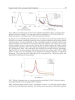
Fig. 9. Decoded BER of LDPC code over GF(8).
Fig. 10. w-Way interleave of (k + r, k) systematic code.
4. Generate a temporary decoded word u
=(
u
0
,
u
1
, ,
u
n−1
) using
Q
j
(x)=f
x
j
×
∏
I∈{I|e
I,j
∈E}
R
I,j
(x) ,
where x
∈ GF(q) and
u
j
= argmax
x∈GF(q)
Q
j
(x).
5. Calculate syndrome s
= Hu
T
.Ifs= o,thenoutputu as a decoded word, and terminate.
6. If the number of iterations i s greater than a predetermined threshold, then terminate with
uncorrectable error detection; otherwise go to step 2.
5.6 Nonbinary LDPC code for flash memory
The following evaluates the decoded BER of the nonbinary LDPC codes for a channel model
of 8-level cell flash memory ( Maeda & Kaneko, 2009), where the threshold voltages are
hypothesized as μ
0
= −3.0000, μ
1
= −2.0945, μ
2
= −1.2795, μ
3
= −0.4645, μ
4
= 0.3505, μ
5
=
1.1655, μ
6
= 1.9805, and μ
7
= 3.0000. These threshold voltages are determined to minimize the
raw BER under the condition that μ
0
= −3.0000, μ
Q−1
= 3.0000, and the standard deviation
σ
i
of P
i
(v) is given as σ
i
= σ for i ∈{1,2, ,Q −2}, σ
0
= 1.2σ,andσ
Q−1
= 1.5σ.
The decoded BER is calculated by decoding 100,000 words, where the maximum number of
iterations in the SPA is 200. Figure 9 illustrates the relation between the standard deviation
σ and the decoded BER of nonbinary LDPC codes over GF
(8) having code rates 1/2 and
5/8. The decoded BER is evaluated for the code length 8000, where the c olumn weights of
the p a rity-check matrix are 2,3, and 2.5. This fi gure also shows the decoded BER of binary
irregular LDPC code. This figure says t hat the nonbinary LDPC codes have lower BER than
binary irregular LDPC co des, and the nonbinary codes with column weight w
= 2.5 give the
lowest BER in many cases.
6. Combination of error control codes
6.1 Fundamental techniques
Interleaving: Interleaving is an effective technique to correct burst errors. Figure 10
illustrates the w-way interleave of a
(k + r, k) systematic code. Here, information word
of length wk is interleaved to generate w information subwords of length k,whichare
53
Error Control Coding for Flash Memory
24 Will-be-set-by-IN-TECH
Fig. 11. Product/concatenated code using systematic block codes.
independently encoded by the
(k + r, k) systematic code. Then, the generated check bits are
interleaved and appended to the information word. If the
(k + r, k) code can correct burst l-bit
errors, then the interleaved code can correct burst wl-bit errors.
Product code: Product code is defined using two block codes over GF
(q),thatis,(k
1
+
r
1
, k
1
) code C
1
and (k
2
+ r
2
, k
2
) code C
2
, as illustrated in Fig. 11(a). Information part is
expressed as a k
1
×k
2
matrix over GF(q). Each column of the i nformation part is encoded by
C
1
, and then each row o f the obtained (k
1
+ r
1
) ×k
2
matrix is encoded by C
2
. The minimum
distance of the p roduct code is d
= d
1
×d
2
,whered
1
and d
2
are the minimum distances of C
1
and C
2
, respectively.
Concatenated code: Concatenated code is defined using two block codes C
1
and C
2
,where
C
1
is a (k
1
+ r
1
, k
1
) code over GF(q
m
),andC
2
is a (k
2
+ r
2
, k
2
) code over GF(q),asshownin
Fig. 11(b). Information part is expressed as a K
1
×k
2
matrix, where K
1
= k
1
×m.Eachcolumn
of the information part, which is regarded as a vector of length k
1
over GF(q
m
),isencoded
by C
1
, and then each row of the obtained (K
1
+ R
1
) × k
2
matrix over GF(q) is encoded by C
2
,
where R
1
= r
1
× m. For example, we can construct the concatenated code using a RS code
over GF
(2
8
) as C
1
and a binary LDPC code as C
2
, by which bursty decoding failure of the
LDPC code C
2
can be corrected using the RS code C
1
.
6.2 Three-level coding for solid-state drive
The following outlines a three-level error control coding suitable for the SSD (Kaneko et al.,
2008), where the SSD is assumed to have N memory chips accessed in parallel. A cluster
is defined as a group of N pages stored in the N memory chips, where the pages have
same memory address, and is read or stored s imultaneously. Let
(D
0
, D
1
, ,D
N−2
) be the
information word, where D
i
is a binary k × b matrix. This information wo rd is encoded as
follows.
1. First level coding: Generate a parity-check segment as P
= D
0
⊕ D
1
⊕···⊕D
N−2
,where
P is a binary k
×b matrix and ⊕ denotes matrix addition over GF(2).
2. Second level coding: Let d
=(d
0
, d
1
, ,d
N−2
, p) be a binary row vector with length kN,
where d
i
=(d
i,0
⊕ d
i,1
⊕···⊕d
i,b−1
)
T
and p =(p
0
⊕ p
1
⊕···⊕p
b −1
)
T
.Encoded by
the code C
CL
to generate the shared-check s egment Q =(Q
0
, Q
1
, ,Q
N−1
) having r
0
bN
bits, where Q
i
=[q
i,0
q
i,1
q
i,b−1
] is a binary r
0
× b matrix for i ∈{0, 1, . . . , N − 1}.
Here,thecheckbitsofC
CL
are expressed as a row vector with length r
0
bN bits, that is,
(q
T
0,0
, q
T
0,1
, ,q
T
0,b−1
, q
T
1,0
, ,q
T
N−1,b−1
). Then, for i ∈{0, 1, . . . , N − 2}, append Q
i
to the
bottom of D
i
, and also append Q
N−1
to the bottom of P .
54
Flash Memories
Error Control Coding for Flash Memory 25
Fig. 12. Encoding process of three level ECC for SSD.
3. Third level coding: For i
∈{0,1, ,N −2} and j ∈{0,1, . . . , b −1},encode
d
i,j
q
i,j
by
code C
PG
to generate check bits r
i,j
,whered
i,j
, q
i,j
,andr
i,j
are binary column vectors with
lengths k, r
0
,andr
1
, respectively. Similarly, for j ∈{0, 1, . . . , b − 1},encode
p
j
q
N−1,j
by
the code C
PG
to generate check bi ts r
N−1,j
,wherep
j
, q
N−1,j
,andr
N−1,j
are binary column
vectors with lengths k,r
0
,andr
1
, respectively.
The above encoding process generates encoded page U
i
as shown in Fig. 12.
7. References
Lin, S. & Costello, D . J. Jr. (2004). Error Control Coding, Pearson Prentice Hall, 0-13-042672-5,
New Jersey.
Fujiwara, E. (2006). Code Design for Dependable Systems –Theory and Practical Applications–,
Wiley-Interscience, 0-471-75618-0, New Jersey.
Muroke, P. ( 2006). Flash Memory Field Failure Mechanisms, Proc. 44th Annual International
Reliability Physics Symposium, pp. 313–316, San Jose, March 2006, IEEE, New Jersey.
Mohammad, M. G.; Saluja, K. K. & Yap, A. S. (2001). Fault Models and Test Procedures for
Flash Memory Disturbances, Journal of Electronic Testing: Theory and Applications,Vol.
17, pp. 495–508, 2001.
Mielke, N.; Marquart, T.; Wu, N.; Kessenich, J.; Belgal, H.; Schares, E.; Trivedi, F.; Goodness,
E. & Nevill, L. R. (2008). Bit Error Rate in NAND F l ash Memories, Proc. 46th Annual
International Reliability Physics Symposium, pp. 9–19, Phenix, 2008, IEEE, New Jersey.
Ielmini, D.; Spinelli, A. S. & Lacaita, A. L. (2005). Recent Developments on Flash Memory
Reliability, Microelectronic Engineering, Vol. 80, pp. 321–328, 2005.
Chimenton, A.; Pellati, P. & Olivo, P. ( 2003). Overerase Phenomena: An Insight Into Flash
Memory Reliability, Proceedings of the IEEE, Vol. 91, no. 4, pp. 617–626, April 2003.
Claeys, C.; Ohyama, H.; Simoen, E.; Nakabayashi, M. and Ko bayashi, K, ( 2002). Radiation
Damage in Flash Memory Cells, Nuclear Instruments and Methods in Physics Research
B, Vol. 186, pp. 392–400, Jan. 2002.
Oldham,T.R.;Friendlich,M.;Howard,Jr.,J.W.;Berg,M.D.;Kim,H.S.;Irwin,T.L.&LaBel,
K. A. (2007). TID and SER Response of an Advanced Samsung 4Gb NAND Flash
Memory, Proc. IEEE Radiation Effects Data Workshop on Nuclear and Space Radiation
Effect Conf, pp. 221–225, July 2007.
55
Error Control Coding for Flash Memory
26 Will-be-set-by-IN-TECH
Bagatin, M .; Cellere, G.; Gerardin, S.; Paccagnella, A.; Visconti, A. & Beltrami, S. (2009). TID
Sensitivity of NAND Flash Memory Building Blocks, IEEE Trans. Nuclear Science,Vol.
56, No. 4, pp. 1909–1913, Aug. 2009.
Witzke, K. A. & Leung, C. (1985). A Comparison of Some Error Detecting CRC Code
Standards, IEEE Trans. Communications, Vol. 33, No . 9, pp. 996–998, Sept. 1985.
Gallager, R . G (1962). Low Density Parity Check Codes, IRE Trans. Information Theory,Vol.8,
pp. 21–28, Jan. 1962.
Moreira, J. C. & Farrell, P. G. (2006). Essentials of Error-Control Coding, Wiley, 0-470-02920-X,
West Sussex.
Richardson, T. J.; Shokrollahi, M. A. & Urbanke, R. L. (2001). Design of Capacity-Approaching
Irregular Low-Density Parity-Check C odes, IEEE Trans. Information Theory, Vol. 47,
No. 2, pp.619–637, Feb. 2001.
IEEE Std 802.11n-2009, Oct. 2009.
IEEE Std 802.16-2009, May 2009.
IEEE Std 802.15.3c-2009, Oct. 2009.
Davey, M. C. & MacKay, D. (1998). Low-Density Parity-Check Codes over GF
(q), IEEE
Communications Letters, Vol. 2, No. 6, pp. 165–167, June 1998.
Zhou, B.; Kang, J.; Tai, Y. Y.; Lin, S. & Ding, Z. (2009) High Pe rformance Non-Binary
Quasi-Cyclic LDPC Codes on Euclidean Geometry, IEEE Trans. Communications, Vol.
57, No. 5, pp. 1298–1311, May 2009.
Li, G.; Fair, I , J. & Krzymien, W. A. (2009). Density Evolution for Nonbinary LDPC Codes
Under Gaussian Approximation, IEEE Trans. Information Theory, Vol. 55, No. 3, pp.
997–1015, March 2009.
Song, H. & Cruz, J. R. (2003). Reduced-Complexity Decoding of Q-Ary LDPC codes for
Magnetic Decoding, IEEE Trans. Magnetics, Vol. 39, No. 3, pp. 1081–1087, March 2003.
Maeda, Y. & Kaneko, H. (2009). Error Control Coding for Multilevel Cell Flash Memories
Using Nonbinary Low-Density Parity-Check Codes, Proc. IEEE Int. Symp. Defect and
Fault Tolerance in VLSI Systems, pp. 367–375, Oct. 2009.
Kaneko, H.; Matsuzaka, T. & Fujiwara, E. (2008). Three-Level Error Control C oding for
Dependable Solid-State Drives. Proc. IEEE Pacific Rim International Symposium on
Dependable Computing, pp. 281–288, Dec. 2008.
56
Flash Memories
3
Error Correction Codes and Signal
Processing in Flash Memory
Xueqiang Wang
1
, Guiqiang Dong
2
, Liyang Pan
1
and Runde Zhou
1
1
Tsinghua University,
2
Rensselaer Polytechnic Institute,
1
China
2
USA
1. Introduction
This chapter is to introduce NAND flash channel model, error correction codes (ECC) and
signal processing techniques in flash memory.
There are several kinds of noise sources in flash memory, such as random-telegraph noise,
retention process, inter-cell interference, background pattern noise, and read/program
disturb, etc. Such noise sources reduce the storage reliability of flash memory significantly.
The continuous bit cost reduction of flash memory devices mainly relies on aggressive
technology scaling and multi-level per cell technique. These techniques, however, further
deteriorate the storage reliability of flash memory. The typical storage reliability
requirement is that non-recoverable bit error rate (BER) must be below 10
-15
. Such stringent
BER requirement makes ECC techniques mandatory to guarantee storage reliability. There
are specific requirements on ECC scheme in NOR and NAND flash memory. Since NOR
flash is usually used as execute in place (XIP) memory where CPU fetches instructions
directly from, the primary concern of ECC application in NOR flash is the decoding latency
of ECC decoder, while code rate and error-correcting capability is more concerned in NAND
flash. As a result, different ECC techniques are required in different types of flash memory.
In this chapter, NAND flash channel is introduced first, and then application of ECC is
discussed. Signal processing techniques for cancelling cell-to-cell interference in NAND
flash are finally presented.
2. NAND flash channel model
There are many noise sources existing in NAND flash, such as cell-to-cell interference,
random-telegraph noise, background-pattern noise, read/program disturb, charge leakage
and trapping generation, etc. It would be of great help to have a NAND flash channel model
that emulates the process of operations on flash as well as influence of various
program/erase (PE) cycling and retention period.
2.1 NAND flash memory structure
NAND flash memory cells are organized in an array->block->page hierarchy, as illustrated
in Fig. 1., where one NAND flash memory array is partitioned into many blocks, and each
Flash Memories
58
block contains a certain number of pages. Within one block, each memory cell string
typically contains 16 to 64 memory cells.
Fig. 1. Illustration of NAND flash memory structure.
All the memory cells within the same block must be erased at the same time and data are
programmed and fetched in the unit of page, where the page size ranges from 512-byte to
8K-byte user data in current design practice. All the memory cell blocks share the bit-lines
and an on-chip page buffer that holds the data being programmed or fetched. Modern
NAND flash memories use either even/odd bit-line structure, or all-bit-line structure. In
even/odd bit-line structure, even and odd bit-lines are interleaved along each word-line and
are alternatively accessed. Hence, each pair of even and odd bit-lines can share peripheral
circuits such as sense amplifier and buffer, leading to less silicon cost of peripheral circuits.
In all-bit-line structure, all the bit-lines are accessed at the same time, which aims to trade
peripheral circuits silicon cost for better immunity to cell-to-cell interference. Moreover,
relatively simple voltage sensing scheme can be used in even/odd bit-line structure, while
current sensing scheme must be used in all-bit-line structure. For MLC NAND flash
memory, all the bits stored in one cell belong to different pages, which can be either
simultaneously programmed at the same time, referred to as full-sequence programming, or
sequentially programmed at different time, referred to as multi-page programming.
2.2 NAND flash memory erase and program operation model
Before a flash memory cell is programmed, it must be erased, i.e., remove all the charges
from the floating gate to set its threshold voltage to the lowest voltage window. It is well
known that the threshold voltage of erased memory cells tends to have a wide Gaussian-like
distribution. Hence, we can approximately model the threshold voltage distribution of
erased state as
(1)
Error Correction Codes and Signal Processing in Flash Memory
59
where
and are the mean and standard deviation of the erased state.
Regarding memory programming, a tight threshold voltage control is typically realized by
using incremental step pulse program (ISPP), i.e., memory cells on the same word-line are
recursively programmed using a program-and-verify approach with a stair case program
word-line voltage V
pp
, as shown in Fig.2.
Fig. 2. Control-gate voltage pulses in program-and-verify operations.
Under such a program-and-verify strategy, each programmed state (except the erased state)
associates with a verify voltage that is used in the verify operations and sets the target
position of each programmed state threshold voltage window. Denote the verify voltage of
the target programmed state as
, and program step voltage as . The threshold voltage
of the programmed state tends to have a uniform distribution over . Denote
and for the k-th programmed state as and . We can model the ideal
threshold voltage distribution of the k-th programmed state as:
(2)
The above ideal memory cell threshold voltage distribution can be (significantly) distorted in
practice, mainly due to PE cycling effect and cell-to-cell interference, which will be
discussed in the following.
2.3 Effects of program/erase cycling
Flash memory PE cycling causes damage to the tunnel oxide of floating gate transistors in
the form of charge trapping in the oxide and interface states, which directly results in
threshold voltage shift and fluctuation and hence gradually degrades memory device noise
margin. Major distortion sources include
1. Electrons capture and emission events at charge trap sites near the interface developed
over PE cycling directly result in memory cell threshold voltage fluctuation, which is
referred to as random telegraph noise (RTN);
2. Interface trap recovery and electron detrapping gradually reduce memory cell
threshold voltage, leading to the data retention limitation.
RTN causes random fluctuation of memory cell threshold voltage, where the fluctuation
magnitude is subject to exponential decay. Hence, we can model the probability density
function
of RTN-induced threshold voltage fluctuation as a symmetric exponential
function:
Flash Memories
60
(3)
Let N denote the PE cycling number,
scales with in an approximate power-law
fashion, i.e.,
is approximately proportional to .
Threshold voltage reduction due to interface trap recovery and electron detrapping can be
approximately modeled as a Gaussian distribution
. Both and scale with N in
an approximate power-law fashion, and scale with the retention time
in a logarithmic
fashion. Moreover, the significance of threshold voltage reduction induced by interface trap
recovery and electron detrapping is also proportional to the initial threshold voltage
magnitude, i.e., the higher the initial threshold voltage is, the faster the interface trap
recovery and electron detrapping occur and hence the larger threshold voltage reduction
will be.
2.4 Cell-to-cell interference
In NAND flash memory, the threshold voltage shift of one floating gate transistor can
influence the threshold voltage of its adjacent floating gate transistors through parasitic
capacitance-coupling effect, i.e. one float-gate voltage is coupled by the floating gate
changes of the adjacent cells via parasitic capacitors. This is referred to as cell-to-cell
interference. As technology scales down, this has been well recognized as one of major noise
sources in NAND flash memory. Threshold voltage shift of a victim cell caused by cell-to-
cell interference can be estimated as
(4)
where
represents the threshold voltage shift of one interfering cell which is
programmed after the victim cell, and the coupling ratio is defined as
(5)
where is the parasitic capacitance between the interfering cell and the victim cell, and
is the total capacitance of the victim cell. Cell-to-cell interference significance is
affected by NAND flash memory bit-line structure. In current design practice, there are two
different bit-line structures, including conventional even/odd bit-line structure and
emerging all-bit-line structure. In even/odd bit-line structure, memory cells on one word-
line are alternatively connected to even and odd bit-lines and even cells are programmed
ahead of odd cells in the same wordline. Therefore, an even cell is mainly interfered by five
neighboring cells and an odd cell is interfered by only three neighboring cells, as shown in
Fig. 3. Therefore, even cells and odd cells experience largely different amount of cell-to-cell
interference. Cells in all-bit-line structure suffers less cell-to-cell inference than even cells in
odd/even structure, and the all-bit-line structure can effectively support high-speed current
sensing to improve the memory read and verify speed. Therefore, throughout the remainder
of this paper, we mainly consider NAND flash memory with the all-bit-line structure.
Finally, we note that the design methods presented in this work are also applicable when
odd/even structure is being used.
Error Correction Codes and Signal Processing in Flash Memory
61
Fig. 3. Illustration of cell-to-cell interference in even/odd structure: even cells are interfered
by two direct neighboring cells on the same wordline and three neighboring cells on the
next wordline, while odd cells are interfered by three neighboring cells on the next
wordline.
2.5 NAND flash memory channel model
Based on the above discussions, we can approximately model NAND flash memory device
characteristics as shown in Fig. 4, using which we can simulate memory cell threshold
voltage
distribution and hence obtain memory cell raw storage reliability.
),(
ee
r
),(
dd
t
pp
V
Fig. 4. Illustration of the approximate NAND flash memory device model to incorporate
major threshold voltage distortion sources.
Based upon the model of erase state and ideal programming, we can obtain the threshold
voltage distribution function p
p
(x) right after ideal programming operation. Recall that p
pr
(x)
denotes the RTN distribution function, and let p
ar
(x) denote the threshold voltage
distribution after incorporating RTN, which is obtained by convoluting p
p
(x) and p
r
(x), i.e.,
(6)
The cell-to-cell interference is further incorporated based on the model of cell-to-cell
interference. To capture inevitable process variability, we set both the vertical coupling ratio
and diagonal coupling ratio as random variables with tailed truncated Gaussian distribution:
(7)
where
and are the mean and standard deviation, and C
C
is chosen to ensure the
integration of this tail truncated Gaussian distribution equals to 1. In all the simulations in
this section, we set
and .
Flash Memories
62
Let p
ac
(x) denote the threshold voltage distribution after incorporating cell-to-cell
interference. Denote the retention noise distribution as p
t
(x). The final threshold voltage
distribution p
f
(x) is obtained as
(8)
The above presented approximate mathematical channel model for simulating NAND flash
memory cell threshold voltage is further demonstrated using the following example.
Example 1: Let us consider 2bits/cell NAND flash memory. Normalized
and of the
erased state are set as 1.4 and 0.35, respectively. For the three programmed states, the
normalized program step voltage
is 0.2, and the normalized verify voltages V
p
are 2.6,
3.2 and 3.93, respectively. For the RTN distribution function, we set the parameter
, where equals to 0.00025. Regarding to cell-to-cell interference, we set the
ratio between the means of and as 0.08 and 0.0048, respectively. For the function
to capture trap recovery and electron detrapping during retention, we set that
scales with
and scales with , and both scale with , where denotes
the memory retention time and is an initial time and can be set as 1 hour. In addition, as
pointed out earlier, both and also depend on the initial threshold voltage. Hence we
set that both approximately scale , where is the initial threshold voltage, and
and are constants. Therefore, we have
(9)
where we set
, , , and . Accordingly, we
carry out Monte Carlo simulations to obtain
Fig. 5. Simulated results to show the effects of RTN, cell-to-cell interference, and retention on
memory cell threshold voltage distribution after 10K PE cycling and 10-year retention.
Error Correction Codes and Signal Processing in Flash Memory
63
Fig. 6. Simulated threshold voltage distribution after 100 PE cycling and 1-month retention
and after 10K PE cycling and 10-year retention, which clearly shows the dynamics inherent
in NAND flash memory characteristics.
Fig. 5 shows the cell threshold voltage distribution at different stages under 10K PE cycling
and with 10-year storage period. The final threshold voltage distributions after 100 PE
cycling and 1 month storage and after 10K PE cycling and 10 years storage are shown in Fig.
6. Fig. 7 presents the evolution of simulated raw BER with program/erase cycling.
0 0.2 0.4 0.6 0.8 1 1.2 1.4 1.6 1.8 2
x 10
4
10
-4
10
-3
10
-2
10
-1
P/E cycling
Raw BER
Fig. 7. The evolution of raw BER with program/erase cycling under 10-year storage period.
3. Basics of error correction codes
In the past decades, error correction codes (ECC) have been widely adapted in various
communication systems, magnetic recording, compact discs and so on. The basic scheme of
ECC theory is to add some redundancy for protection. Error correction codes are usually
Flash Memories
64
divided into two categories: block codes and convolution codes. Hamming codes, Bose-
Chaudur-Hocquenghem(BCH) codes, Reed-Solomon(RS) codes, and Low-density parity-
check (LDPC) codes are most notable block codes and have been widely used in
communication, optical, and other systems.
The encoding/decoding scheme of a block code in a memory is shown in Fig. 8. When any
k-bit information data is written to flash memory, an encoder circuit generates the parity
bits, adds these parity bits to the k-bit information data and creates a n-bit codeword. Then
the whole codeword is written in and stored on a page of the memory array. During the
reading operation, a decoder circuit searches errors in a codeword, and corrects the
erroneous bits within its error capability, thereby recovering the codeword.
Fig. 8. ECC encoding and decoding system in a flash memory
Current NOR flash memory products use Hamming code with only 1-bit error correction.
However, as raw BER increases, 2-bit error corretion BCH code becomes a desired ECC.
Besides, in current 2b/cell NAND flash memory. BCH codes are widely employed to
achieve required storage reliability. As raw BER soars in future 3b/cell NAND flash
memory, BCH codes are not sufficient anymore, and LDPC codes become more and more
necessary for future NAND flash memory products.
3.1 Basics of BCH codes
BCH codes were invented through independent researches by Hocquenghen in 1959 and by
Bose and Ray-Chauduri in 1960. Flash memory uses binary primitive BCH code which is
constructed over the Galois fields GF(2
m
). Galois field is a finite field in the coding theory
and was first discovered by Evariste Galois. In the following, we will recall some algebraic
notions of GF(2
m
).
Definition 3.1 Let α be an element of GF(2
m
), α is called primitive element if the smallest
natural number n that satisfies α
n
=1 equals 2
m
-1, that is, n=2
m
-1.
Theorem 3.1 Every none null element of GF(2
m
) can be expressed as power of primitive
element α, that is, the multiplicative group GF(2
m
) is cyclic.
Definition 3.2 GF(2
m
)[x] is indicated as the set of polynomials of any degree with
coefficients in GF(2
m
). An irreducible polynomial p(x) in GF(2
m
)[x] of degree m is called
primitive if the smallest natural number n, such that x
n
–1 is a multiple of p(x), is n=2
m
–1.
In fact, if p(x)=x
m
+a
m-1
x
m–1
+…+a
1
x+a
0
is a primitive polynomial in GF(p)[x] and α is one of its
roots, then we have
21
01 2 1
mm
m
aaa a a
(10)
Error Correction Codes and Signal Processing in Flash Memory
65
Equation (10) indicates that each power of α with degree larger than
m can be converted
to a polynomial with degree
m-1 at most. As an example, some elements in the field
GF(2
4
), their binary representation, and according poly representation forms are shown in
Table 1.
Element
Binary
representation
Polynomial
representation
0 0000 0
α
0
1000 1
α
1
0100 α
α
3
0001 α
3
α
4
1100 1+α
α
5
0110 α+α
2
α
6
0011 α
2
+α
3
Table 1. Different representations of elements over GF(2
4
)
Based on the Galois fields GF(2
m
), the BCH(n, k) code is defined as
Codeword length:
n = 2
m
-1
Information data length:
k
2
m
-mt
In a BCH code, every codeword polynomial c(x) can be expressed as c(x)=m(x)g(x), where
g(x) is the generator polynomial and m(x) is the information polynomial.
Definition 3.3 Let α be the primitive element of GF(2
m
). Let t be the error correction
capability of BCH code. The generator polynomial g(x) of a primitive BCH code is the
minimal degree polynomial with root: α, α
2
,…α
t
. g(x) is given by
01 2
() { (), (), ()}
d
gx LCM x x x
(11)
Where
Ψ
i
is the minimal polynomial of α
i
.
Generally, the BCH decoding is much more complicated than the encoding. A typical
architecture of BCH code application in a flash memory is presented in Fig. 9.
i
Fig. 9. Architecture of BCH code application in a flash memory
3.1.1 BCH encoding
For a BCH(n,k) code, assuming its generator polynomial is
g(x), and the polynomial of the
information to be encoded is m(x) with degree of k-1. The encoding process is as follows:
First, the message
m(x) is multiplied by x
n-k
, and then divided by g(x), thereby obtaing a
quotient
q(x) and a remainder r(x) according to equation (12). The remainder r(x) is the
polynomial of the parity information; hence the desired parity bits can be obtained.
Flash Memories
66
() ()
()
() ()
nk
mx x rx
qx
gx gx
(12)
As mentioned above, any codeword of BCH code is a multiple of the generator polynomial.
Therefore, an encoded codeword
c(x) can be expressed as:
() () ()
nk
cx mx x rx
(13)
3.1.2 BCH decoding
Generally the decoding procedure for binary BCH codes includes three major steps, which is
shown in Fig. 9.
Step 1: Calculating the syndrome S.
Step 2: Determining the coefficients of the error-location polynomial.
Step 3: Finding the error location using Chien Search and correcting the errors.
During the period of data storage in flash memory, the repeated program/erase (P/E) cycles
may damage the stored information; thereby some errors occur in the read operation. The
received codeword can be expressed as r(x) = c(x) + e(x) with the error polynomial
representation e(x) = e
0
+ e
1
x + … e
n-1
x
n-1
The first step in the BCH decoding is to calculate 2t syndromes with the received r(x). The
computation is given by
2
()
()
( ) 1
() ()
i
i
ii
Sx
rx
Qx
f
or i t
xx
(14)
Where Ψ
i
is the minimal polynomial of element α
i
,
t is the error numbers in codeword. S
i
(x)
is called syndrome. Since Ψ
i
(α
i
)=0, the syndrome can also be obtained as S
i
(α
i
) = r(α
i
).
S
i
(α
i
) = r(α
i
)
(15)
From equation (14), it can be seen that the syndrome calculation in the BCH decoding is
similar to the encoding process in equation (12). Hence, they both employ the linear
feedback shift register (LFSR) circuit structure.
The next step is to compute the coefficients of the error-location polynomial using the
obtained syndrome values. The error-location polynomial is defined as
2
12
1()
t
t
xxxx
(16)
Where and
i
(1 i t) is the required coefficient.
There are two main methods to compute the coefficients, one is Peterson method and the
other is Berlekamp-Massey algorithm. In the following sections, we will discuss and employ
both methods for error correction in different types of flash memory.
The last step of BCH decoding is Chien search. Chien search is employed to search for the
roots of the error locator polynomial. If the roots are found
(
i
) =0 for 0
i
n-1, then the
error location is
n-1-i in the codeword. It should be noted that the three modules of a BCH
decoder is commonly designed with three pipeline stages, leading to high throughput of the
BCH decoding.
Error Correction Codes and Signal Processing in Flash Memory
67
3.2 LDPC code
Low-density parity-check (LDPC) codes can provide near-capacity performance. It was
invented by Gallager in 1960, but due to the high complexity in its implementation, LDPC
codes had been forgotten for decades, until Mackey rediscovered LDPC codes in the 1990s.
Since then LDPC codes have attracted much attention.
A LDPC code is given by the null space of a sparse
mxn ‘low-density’ parity-check matrix H.
Regular LDPC codes have identical column weight and identical row weight. Each row of H
represents one parity check. Define each row of H as check node (CN), and each column of
H as variable node (VN). A LDPC code can be represented by Tanner graph, which is a
bipartite graph and includes two types of nodes:
n variable nodes and m check nodes. In
Tanner graph, the
i-th CN is connected to j-th VN, if h
i,j
=1.
Consider a (6, 3) linear block code with H matrix as
H
=
1 1 1 0 1 0
1 1 0 1 0 1
1 0 1 1 1 1
The corresponding Tanner graph is shown in Fig. 10.
The performance of LDPC code depends heavily on parity-check matrix H. Generally
speaking, LDPC code with larger block length, larger column weight and larger girth trends
to have better performance. In Tanner graph, a cycle is defined as a sequential of edges that
form a closed path. Short cycles degrade the performance of LDPC codes, and length of the
shortest cycle in Tanner graph is named as girth.
Fig. 10. The Tanner graph for the given (6, 3) linear block code.
There have been lots of methods to construct parity-check matrix. To reduce the hardware
complexity of LDPC encoder and decoder, quasi-cyclic (QC) LDPC code was proposed and
has widely found its application in wireless communication, satellite communicate and
hard-disk drive.
As for LDPC decoding, there are several iterative decoding algorithms for LDPC codes,
including bit-flipping (BF) like decoding algorithms and soft-decision message-passing
decoding algorithms. Among all BF-like decoding, BF and candidate bit based bit-flipping
(CBBF) can work with only hard-decision information. Other BF-like decoding require soft-
decision information, which incurs large sensing latency penalty in flash memory devices as
discussed later, though they may increase the performance a little bit.
Soft-decision message passing algorithm, such as Sum-product algorithm (SPA), could
provide much better performance than BF-like decoding, upon soft-decision information.
However, the complexity of SPA decoding is very high. To reduce the decoding complexity,
min-sum decoding was proposed, with tolerable performance loss. Readers can refer to
“Channel Codes: Classical and Modern” by Willian E. Ryan and Shu Lin.
Flash Memories
68
4. BCH in NOR flash memory
Usually NOR flash is used for code storage and acts as execute in place (XIP) memory where
CPU fetches instructions directly from memory. The code storage requires a high-reliable
NOR flash memory since any code error will cause a system fault. In addition, NOR flash
memory has fast read access with access time up to 70ns. During read operation, an entire
page, typical of 256 bits, is read out from memory array, and the ECC decoder is inserted in
the critical data path between sense amplifiers and the page latch. The fast read access
imposes a stringent requirement on the latency of the ECC decoder (required <10%
overhead), and the ECC decoder has to be designed in combinational logic. As a result,
decoding latency becomes the primary concern for ECC in NOR Flash memory.
Traditionally, hamming code with single-error-correction (SEC) is applied to NOR flash
memory since it has simple decoding algorithm, small circuit area, and short-latency
decoding. However, in new-generation 3xnm MLC NOR flash memory, the raw BER will
increase up to 10
-6
while application requires the post-ECC BER be reduced to 10
-12
below.
From Fig. 11, it is clear that hamming code with
t=1 is not sufficient anymore, and double-
error-correction (DEC) BCH code gains more attraction in future MLC NOR flash memory.
However, the primary issue with DEC BCH code applied in NOR flash is the decoding
latency. In the following, a fast and adaptive DEC BCH decoding algorithm is proposed and
a high-speed BCH(274,256,2) decoder is designed for NOR flash memory.
10
-8
10
-7
10
-6
10
-5
10
-4
10
-3
10
-2
10
-22
10
-20
10
-18
10
-16
10
-14
10
-12
10
-10
10
-8
10
-6
10
-4
10
-2
BER After ECC
Raw BER
no ECC
Hamming code
DEC BCH code
Fig. 11. BER curves of different ECC in NOR flash memory with 256-bit page size
4.1 High-speed DEC BCH decoding algorithm
First we employ equation equation (15) for high-speed syndrome computation. The entire
expression of syndromes is
22
12 2 01
121 21
,
1 1 . 1
( ) ( ) . ( )
( , , ) ( . . . )
. . . .
( ) ( ) . ( )
t
T
tn
nn tn
SS S rH rr r
(17)