Flash Memories Part 9 pdf
Bạn đang xem bản rút gọn của tài liệu. Xem và tải ngay bản đầy đủ của tài liệu tại đây (1.08 MB, 20 trang )
Adaptively Reconfigurable Controller
for the Flash Memor y 13
Fig. 13. Hardware structure of the flash/SRAM PR design
Fig. 14. Flow chart of multiplexing flash/SRAM in Linux
compiled into modules. They will be inserted into the OS kernel when the corresponding
device hardware is configured, or removed when not needed any longer.
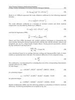
The hardware process scheduler is implemented in a C program. It detects the memory access
requirements on flash or SRAM from either the system interior or external user commands,
and meanwhile manages the work sequence of both types of memories. Figure 14 shows a
flow chart, in which the scheduler alternately loads the flash and the SRAM controller with
context awareness. During the device module reconfiguration, the Linux OS as well as the
remaining hardware system keeps running without breaks. In this figure, steps labeled with
“a - g ” are used to dynamically configure the SRAM controller, and the ones labeled with
149
Adaptively Reconfigurable Controller for the Flash Memory
14 Will-be-set-by-IN-TECH
“A - G” are to load the flash controller. Events marked by the symbol “”aredetected
by the scheduler to trigger hardware context switching. Main switching steps before device
operations include:
1. To save the register context of the to-be-unloaded device in DDR variables if necessary.
2. To remove the driver module of the to-be-unloaded device from the OS.
3. To disconnect the PRR outputs for isolating its unsteady state during active reconfiguration
from the static design.
4. To dynamically load the partial bitstream of the expected controller by initiating the
MST_HWICAP core.
5. To solely reset the newly loaded device controller, and recover its register context if there
exists.
6. To re-enable the PRR outputs, restoring the communication links from the PRR to the static
design.
7. To insert the corresponding device driver in the OS, for the processor access with high-level
application software.
After these steps, the recently equipped controller module becomes ready for memory
accesses on the NO R flash or the SRAM.
In this design, IPC operations can be realized through the third-party shared memory such
as DDR. For example when the system is just powered on, the SRAM LUT initialization data
are retrieved from the nonvolatile flash and buffered in the system DDR memory. After the
flash controller is unloaded and the SRAM controller is activated in the PRR by dynamic
reconfiguration, the LUT data are then migrated into the SRAM chip f or application-specific
computation. The IPC data flow is illustrated in Figure 15.
5.2 Results
Through enabling either the flash controller or the SRAM controller with system
self-awareness, multitasking has been accomplished within a single reconfigurable slot on
the FPGA. Figure 16 demonstrates the rectangular shape of the reserved PR region on a
Virtex-4 FX20 FPGA layout, as well as two controller i mplementations after place-and-route.
The reconfigurable design results in a more efficient utilization of hardware resources, as
listed in Table 1. We understand that both the flash memory controller and the SRAM
controller must be concurrently placed in the static system design, implying a total resource
consumption equivalent to the sum of both device modules. A PR region is reserved in the
reconfigurable design, sufficiently large to accommodate all kinds of needed resources of both
device modules. Moreover, a little more resource margin is added for the place-and-route
convenience of the software tool. In contrast to the conventional static approach, we observe
that the reconfigurable system saves 43.7% LUTs, 33.8% slice registers and 47.9% I/O pads,
with both flash and SRAM services realized. The reduced resource requirement not only
enables to fit a large system design on small FPGA chips for lower hardware cost, but also
makes the I/O pads shared and simplifys the Printed Circuit Board (PCB) routing.
150
Flash Memories
Adaptively Reconfigurable Controller
for the Flash Memor y 15
Fig. 15. Migrating LUT initialization data from the flash memory to the SRAM
(a) The flash implementation in
PRR
(b) The SRAM implementation
in PRR
Fig. 16. Implementation of the flash and the SRAM controller within the PRR on a Virtex-4
FX20 FPGA
6. Conclusion
Based on the FPGA run-time reconfigurability, we present a dynamically reconfigurable
NOR flash controller for embedded designs. This technique is motivated by the operation
occasionality of the flash memory and the resultant programmable resource waste on the
FPGA, when adopting the conventional static development approach. We discuss the
151
Adaptively Reconfigurable Controller for the Flash Memory
16 Will-be-set-by-IN-TECH
Resources Static flash
controller
Static SRAM
controller
Total PRR Resource
saving
4-input
LUTs
923 954 1877 1056 43.7%
Slice
Flip-Flops
867 728 1595 1056 33.8%
I/O pads 56 61 117 61 47.9%
Table 1. Resource utilization of the static/reconfigurable flash/SRAM designs
design framework of adaptively reconfigurable peripherals in this chapter, concerning various
aspects in hardware and software. In the practical experiment, a reserved reconfigurable
slot is time-shared by the flash memory controller and an SRAM controller. Both system
requirements of accessing the flash memory and the SRAM are equally accomplished in the
reconfigurable design, with much less resource utilization of FPGA LUTs, slice registers as
well as I/O pads.
This design technique is not limited to memory controller modules, but can apply to all kinds
of modular devices operating exclusively. In addition, system functionalities can be later
extended by adding more functional modules to time-share a same reconfigurable slot. It not
only enhances the resource utilization efficiency on FPGAs, but also enables the possibility of
future firmware upgrade without hard ware modification.
7. Acknowledgment
This work was supported in part by BMBF under contract Nos. 06GI9107I and 06GI9108I,
FZ-Jülich under contract No. COSY-099 41821475, HIC for FAIR, and WTZ: C HN 06/20. The
authors also thank Xilinx Inc. for the software donation.
8. References
Ahmadinia, A., Bobda, C., Ding, J., M ajer, M., Te ich, J., Fekete, S. & van der Veen, J. (2005). A
practical approach for circuit routing on dynamic reconfigurable devices, Proceedings
of the IEEE International Workshop on Rapid System Prototyping, pp. 84–90.
Corbet, J., Rubini, A. & Kroah-Hartman, G. (2005). Linux Device Drivers (Third Edition),
O’REILLY & Associates, Inc.
Delorme, J., Nafkha, A., Leray, P. & Moy, C. (2009). New opbhwicap interface for
realtime partial reconfiguration of fpga, Proceedings of the International Conference on
Reconfigurable Computing and FPGAs, pp. 386–391.
Dillien, P. (2009). An overview of fpga market dynamics. SOCcentral webpage.
URL:
Dunlap, C. & Fischaber, T. (2010). Partial reconfiguration user guide. UG702, Xilinx Inc.
Elgindy, H. A., Somani, A. K., Schroeder, H., Schmeck, H. & Spray, A. (1996). Rmb
´
lc a
reconfigurable multiple bus network, Proceedings of the International Symposium on
High-Performance Computer Architecture, pp. 108–117.
Fekete, S., van der Veen, J., Majer, M. & Teich, J. (2006). Minimizing communication cost
for reconfigurable slot modules, Proceedings of the International Conference on Field
Programmable Logic and Applications, pp. 1–6.
152
Flash Memories
Adaptively Reconfigurable Controller
for the Flash Memor y 17
Huang, C. & Hsiung, P. (2008). Software-controlled dynamically swappable hardware design
in partially reconfigurable systems, EURASIP Journal on Embedded Systems 2008: 1–11.
Hubner, M., Schuck, C. & Becker, J. (2006). Elementary block based 2-dimensional dynamic
and partial reconfiguration for virtex-ii fpgas, Proceedings of the International Parallel
and Distributed Processing Symposium.
IBM (2007). 128-bit processor local bus architecture specifications. Version 4.7, IBM Inc.
Ito, T., Mishou, K., Okuyama, Y. & Kuroda, K. (2006). A hardware resource management
system for adaptive computing on dynamically reconfigurable devices, Proceedings
of the Japan-China Joint Workshop on Frontier of Computer Science and Technology,
pp. 196–202.
Kalte, H. & Porrmann, M. (2005). Context saving and restoring for multitasking
in reconfigurable systems, Proceedings of the International Conference on Field
Programmable Logic and Applications, pp. 223–228.
Kao, C. (2005). Benefits o f partial reconfiguration, Xcell Journal Fourth Quarter: 65–67.
Kuon, I. & Rose, J. (2006). Measuring the gap between fpgas and asics, Proceedings of the
International Symposium on Field-Programmable Gate Arrays, ACM Press, pp. 21–30.
Liu, M., Kuehn, W., Lu, Z. & Jantsch, A. (2009). Run-time partial reconfiguration
speed investigation and architectural design space exploration, Proceedings of the
International Conference on Field Programmable Logic and Applications, p p. 498–502.
Liu, M., Lu, Z., Kuehn, W. & Jantsch, A. (2010). Inter-process communications using pipes
in fpga-based adaptive computing, Proceedings of the IEEE Computer Society Annual
Symposium on VLSI, p. 80.
Liu, S., Pittman, R. N. & Forin, A. (2009). Minimizing partial reconfiguration overhead
with fully streaming dma engines and intelligent icap controller, Technical Report
MSR-TR-2009-150, Microsoft Research.
Lu, S., Yiannacouras, P., Suh, T., Kassa, R. & Konow, M. (2008). A desktop computer with a
reconfigurable pentium
, ACM Transactions on Reconfigurable Technology and Systems
1(1): 1–15.
Majer, M ., Teich, J., Ahmadinia, A. & Bobda, C. (2007). The erlangen slot machine:
A dynamically reconfigurable fpga-based computer, The Journal of VLSI Signal
Processing 47(1): 15–31.
So, H. K., Tkachenko, A. & Brodersen, R. (2006). A unified hardware/software runtime
environment for fpga-based reconfigurable computers using borph, Proceedings
of the International Conference on Hardware/Software Codesign and System Synthesis,
pp. 259–264.
Wilton, S., Kafafi, N., Wu, J., Bozman, K., Aken’Ova, V. & Saleh, R. (2005). Design
considerations for soft embedded programmable logic cores, IEEE Journal of
Solid-State Circuits 40(2): 485–497.
Woodhouse, D. (2005). Memory technology device (mtd) subsystem for linux. MTD webpage.
URL: />Xilinx (2004). Two flows for partial reconfiguration: Module based or difference based.
XAPP290, Xilinx Inc.
Xilinx (2006). Plb external memory controller (plb emc) (2.00a). DS418, Xilinx Inc.
Xilinx (2008). Early access partial reconfiguration user guide for ise 9.2.04i. UG208, Xilinx Inc.
Xilinx (2010). Partial reconfiguration user guide. UG702, Xilinx Inc.
153
Adaptively Reconfigurable Controller for the Flash Memory
18 Will-be-set-by-IN-TECH
Zuchowski, P., Reynolds, C., Grupp, R., Davis, S., Cremen, B. & Troxel, B. (2002). A hybrid
asic and fpga architecture, Proceedings of the International Conference on Computer-Aided
Design, pp. 187–194.
154
Flash Memories
8
Programming Flash Memory in Freescale
S08/S12/CordFire MCUs Family
Yihuai Wang and Jin Wu
Soochow University
China
1. Introduction
The features of Flash memory include electrically erasable, no back-up power to protect
data, in-circuit programming, high-density memory, low-cost and so on, which rapidly
increase the using of Flash memory in embedded system.
The programming methods of Flash memory include Programmer Mode and In-Circuit
Programmer Mode. Programmer Mode means erasing/programming Flash by
programming tool (programmer), with the purpose of writing programs into MCU
1
. In-
Circuit Programmer Mode means erasing/programming some region of Flash by MCU’s
internal programs during run time, with the purpose of saving relevant data and preventing
from lost after power off. Take AW60/XS128/MCF52233 in Freescale 8/16/32bits
S08/S12/ColdFire serials’ MCUs for example, we elaborate the In-Circuit Programming
method of Flash memory in this chapter. The programming method of the other MCUs in
the whole Freescale S08/S12/ColdFire MCU family is similar. Besides, we discuss the
protection mechanisms and security operations for AW60/XS128/MCF52233 Flash memory.
Some instances are also provided in this chapter.
1.1 Flash memory characteristics
The most perfect memory should be a high-speed, non-volatile, low-cost and high-density
memory. But only one or several specialties are implemented in general memory. With
the maturity of its technology, flash memory has become an ideal memory in recent years.
It is endowed with characteristics such as electrical erasure, data preservation without
power supply, in-system programming, high storage density, low power consumption
and low cost. These are just what MCU are expecting, because MCU with internal flash
memory introduced in earlier years has some shortages in reliability and stability. With
the maturity of the Flash technology, now more and more above characteristics are
integrated to MCU and become an important part of it. Hence flash memory makes MCU
progress enormously.
Flash memory is really a high-density, high-performance reading/writing memory with
non-volatility, low-power and high-reliability and has the following characteristics
comparing with old solid state memory.
1
MCU—Microcontroller Unit
Flash Memories
156
1. Non-volatility: Flash memory protects data without power supply the same as magnetic
storage.
2. Easy-updating: Comparing with old EPROM
2
, the electrical erasure of flash memory
shortens the programming cycle for developers and makes end users’ updating
memory become true.
3. Low-cost, high-density and reliability: The parameters are much better than EEPROM
(or E2PROM).
1.2 Flash memory program concepts
In many embedded systems, the memory which can protect program parameters and
important data without external power supply is necessary as EEPROM previously was. The
ColdFire MCU family provides the function of in-system programming of flash memory in
user mode instead of EEPROM, hence making the circuit design simpler and cost lower.
However, different from the reading/writing of generic RAM, flash memory operations
need two special processes—Erase and Program. The former, which converts all bits to 1,
consists of mass erase and page erase. The latter, which converts bit to 0, can program only
one word at a time. During erasing and programming, voltage higher than the power is
usually needed and it is generated by Coldfire MCU inner electric charge pump. Besides,
before programming, it should be insured that the program field has not been written after
last erasure. That is, the field is blank (the content is $FF). So generally, erase should be
carried out before perform.
1.3 In-circuit programming concepts of flash memory
In-circuit programming of flash memory in user mode (U-ICP) is a technique by which user
programs stored in flash memory can modify data or programs also stored in the flash
memory during run time. The electrically erasable characteristics of flash memory allow
such programs to execute erase or write functions. This important branch of computer
technology, an outgrowth of embedded systems development, makes it possible to update
embedded programs, provide power-off protection and the recovery of important
parameters, and modify the static parameters of embedded applications. In addition, U-ICP
improves the expansibility and upgradeability of embedded systems. Portions of flash
memory can substitute for the traditional EEPROM functions mentioned above, increasing
system stability. And make the circuit design simpler and cost lower.
U-ICP was introduced to MCU technology by the semiconductor department of Motorola
(now called Freescale) in 2000, and has been widely applied and developed ever since.
However, different from the reading/writing of generic RAM, flash memory operations
need two special processes—Erase and Program. The former, which converts all bits to 1,
consists of mass erase and page erase. The latter, which converts bit to 0, can program only
one word at a time. During erasing and programming, voltage higher than the power is
usually needed and it is generated by Freescale S08/S12/CordFire MCU inner electric
charge pump. Besides, before programming, it should be insured that the program field has
not been written after last erasure. That is, the field is blank (the content is $FF). So
generally, erase should be carried out before perform.
U-ICP can erase and reprogram other regions of flash memory by executing internal flash
functions, but these may also prove unstable at high voltage. This problem, which is indicated
2
EEPROM—Electrically Programmable Read-Only-Memory
Programming Flash Memory in Freescale S08/S12/CordFire MCUs Family
157
in the data sheet of the Freescale S08/S12/CordFire MCU family, has not yet been solved by
hardware design. It can be solved on the software level, by proper design of the U-ICP bottom
driver program. So we describe an embedded software engineering rule that should improve
the stability of the general erase and write functions in U-ICP for any flash device.
2. Programming flash in freescale MC9S08AW60 MCU
The flash memory in-circuit programming implement for 8bit MC9S08AW60 MCU will be
explained in this section, as follows:
2.1 How to operate MC9S08AW60 flash memory
2.1.1 MC9S08AW60 Flash memory-mapping
S08 serials MCUs’ addressable address space is 64Kbyte, which ranges from $0000 ~ $FFFF.
This addressing range is divided into different sectors. Each sector has different function.
The memory map of AW60 MCU is shown in Fig.1, which includes the address distribution
of 2KB RAM
3
, 2 parts of Flash memory and some I/O image registers.
As can be seen from the Fig.1, the Flash memory of AW60 is divided into two parts in this
64K memory address space. These addresses range from $0870~$17FF(3984 bytes) and
$1860~$FFFF(59296 bytes). Among $1860~$FFFF only the addresses range from $1860~
$FFAF can be used to erase and program user program. The addresses range from $FFB0~
$FFBF are the 16 bytes non-volatile registers region and the addresses range from $FFC0~
$FFFF are the 64 bytes interrupt vector region.
Flash memory is organized by page and row in the chip. The size of each page is 512 bytes.
And the size of each row is 64 bytes. There are about 60K bytes of Flash memory address
space in AW60, the page addresses are rounding 512 in $0000~$FFFF. For example, the first
page’s address of Flash memory in the 3984bytes region ($0870~$17FF) is $1000~$11FF,
instead of $0870~$0A6F.
Fig. 1. The memory map of AW60 MCU
3
RAM—Random Access Memory
Flash Memories
158
For S08 serials MCU ( AW60, etc.), we can do mass erasing operation for the Flash memory,
or can erasing one page(512 bytes) from a certain start address. But we can’t only erase a
certain byte or some bytes which are less than 512 bytes. Noting this feature, it is important
for the data arranging. The programming operation of AW60 is based on row (64 bytes). The
data which can be programmed continuously at a time is only within one row. Certainly, the
region that has not been erased can’t be programmed.
As can be seen from the above, in order to program Flash memory, we should prepare a set
of data and move them into RAM, then erase the corresponding region of Flash memory, so
programming operation can be done. Because erasing /programming a certain byte of Flash
memory will influence the follow-up one page, it is necessary to reasonably arrange the
relevant data of erasing region before erasing/programming the Flash.
2.1.2 MC9S08AW60 FLASH registers and control bits
In AW60, Erasing and programming operations relate to registers such as FCDIV、FOPT、
FCNFG、FPROT、FSTAT and FCMD. Their corresponding addresses are $1820、$1821、
$1823、$1824、$1825 and $1826. For the detailed function and use of these registers, please
refer to the Reference Manual “MC9S08AW60 Data Sheet (HCS08 Microcontrollers)”[1].
2.1.3 Flash programming procedure
1. The execution steps of Flash commands
a. Write a data in an address of Flash. The address and data information will be
locked into Flash interface. For blank check command, the data information is an
arbitrary value; For page erase command, the address information is either one of
the address in erase page (512 bytes) addresses; For blank check and mass erase
commands, the address information is either one of the address in flash.
b. Write the commands which are needed to be executed into FCMD.
c. Execute commands. The FCBEF bit of FSTAT register is set, simultaneously execute
the commands in the FCMD.
2. The flowcharts of the Flash programming
When programming flash, we need follow strict timing process. Fig.2 gives the
programming flowchart with the other flash commands ( not include the command “burst
mode byte program”). Writing a byte with burst mode command is very different from the
execution with other commands. Burst mode means a lot of continuous data need to be
written into Flash. Each time a write command has been executed, the writing high voltage
in flash will not be removed, which will speed up the write speed of data; But for other
commands, the high voltage is given to ensure the command executing, and the high
voltage is immediately removed when the command ended. The programming flowchart
with burst mode command is shown in Fig.3.
3. Flash Memory Illegal Operations
In the following processing, an error occurs, and the FACCERR bit is automatically set.
a. Writing the flash memory before initializing FCDIV register.
b. Writing the flash memory while FCBEF is not set.
c. Writing the second command to the FCMD register before executing the previously
written command。
d. After write the flash memory, initializing the other flash control registers in
addition to FCMD.
Programming Flash Memory in Freescale S08/S12/CordFire MCUs Family
159
Fig. 2. AW60 Flash programming flowchart Fig. 3. AW60 Flash burst mode pro
g
rammin
g
flowchart
e. Writing an invalid flash normal mode command to the FCMD register.
f. Try to operate the other registers in addition to FSTAT after finished writing
command values to FCMD.
g. MCU enters into STOP mode when execute the command.
h. When MCU is in secure state, erase pages or write flash memory with background
debug interface (If MCU is in encrypted state, we can only execute blank check or
mass erase commands with background debug interface).
i. Aborting a command write sequence by writing 0 to the FCBEF flag.
2.2 MC9S08AW60 flash memory in-circuit programming instance
We first give the AW60's Flash programming subroutine in this section. Then put forward
the Flash in-circuit programming instance in user mode. And verify the result by the serial
communication mode with PC.
Flash Memories
160
2.2.1 The erasing and programming c language subroutines of flash memory
For the Flash programming subroutines are not solidified in the internal monitoring ROM
4
of AW60, the initial loaded user program should contain the flash erasing and programming
subroutines in order to do in-circuit programming for Flash. Because these subroutines
resident in Flash, when running the erasing/programming subroutines, the whole Flash
region will be added programming voltage that is higher than the normal operating voltage,
which results in instable Flash region’s reading, and may lead to program’s error running.
In order to make the erasing/programming subroutines running normally, these
subroutines should be moved into RAM and run in RAM. Therefore, a buffer should be
opened up in RAM to store these subroutines. The following sample program gives a
convenient method to save the machine codes which are generated by
erasing/programming subroutines in RAM. The machine codes include 57 bytes.
Necessarily, you can directly call these codes to implement the Flash in-circuit
erasing/programming. For the detailed Erasing and Programming subroutines, please refer
to the program in our program directory “ \Flash_Program\S08(AW60)-Flash”
5
. These
subroutines contain the following operations:
1. Some public operation of erasing/programming processing
For the codes of erasing/programming operation must run in RAM, so we write the C
language program according to Fig.2. After being compiled, the corresponding machine
code bytes are saved in the array PGM (volatile unsigned char PGM[57]). Therefore we need
not copy the codes to RAM to realize the erasing/programming operations.
2. Page erasing subroutine (Flash_PageErase)
In this subroutine we should calculate the page’s top address by the page number, and
change the Flash command to erasing command 0x40, then call and execute the erasing
codes.
3. Flash programming subroutine
In this subroutine we calculate the top programming address according to the page number
and page offset, then change the Flash command to erasing command 0x20, and program
flash one byte by one byte.
2.2.2 Programming essentials of erasing /programming subroutines
Using Flash in-circuit programming technology eliminates the need for external EEPROM,
which not only simplify the circuit design, but also improve the stability of system. We
compile the Flash programs and save them in Flash. When you need to use these codes, they
will be copied to RAM. Just because of this special procedure, we put forward the following
notes according to the experience which is accumulated in the actual programming and
debugging, and project development process.
1. There are 57 bytes in RAM to store the erasing/programming machine codes, don’t
forget to calculate when using RAM.
2. The region that has been erased for one time and has not been programmed can be
programmed by calling Flash programming subroutine again, but the region that has
been programmed can’t be programmed again if it hasn’t been erased.
4
ROM—Read Only Memory
5
You can download the program directory “Flash_Program” in our website
( which involves three Flash programming instances in three
subdirectory (“\S08(AW60)-Flash”, “\ S12X(XS128)-Flash” and “\ ColdFire(MCF52233)-Flash”).
Programming Flash Memory in Freescale S08/S12/CordFire MCUs Family
161
3. For we do erasing for one page (512 bytes) each time, so we should arrange the data
reasonably to avoid wrong erasing.
4. The start address of the page should be defined according to the rules of the FPROT
register.
5. It is invalid to do in-circuit programming for the protection block set in FPROT.
2.2.3 Validate flash memory implements
In order to more clearly understand the method of Flash memory in-circuit programming,
we give a flash memory validating project. Its function is as the following: the MCU receives
formatted data from PC
6
by SCI
7
tools and erases, programs or reads its flash memory. The
PC software is any SCI testing tool.
Now, list some flash operating commands using the SCI debug (as shown in Table 1):
Commands Functions
? MCU sends some items to PC
E:8 Erase page 8
R:8:0:4 Read 4 bytes the word 0 of page 8
W:8:0:4:A,C,B,D Write “ACBD” (4 bytes) to the word 0 of page 8
B:8,7,6,5,4,3,2,1 Set the Flash back door key, the password is "87654321"
M:8,7,6,5,4,3,2,1 Verify the Flash back door key, the password is "87654321"
D Delete passwords
U Encryption lift
P:8 Protect block, protect the addresses from 8 to 0xFFFF
Table 1. Flash operating commands using the SCI debug
Above examples only give the program data less than one page (512 bytes).
Only slightly
modify the program, you
can program data that exceeds one page.
2.3 Protection mechanisms and security operations of MC9S08AW60 flash memory
2.3.1 Protection mechanisms
Being a non-volatile memory (NVM), flash memory may be used by programmers to store
some important parameters and data. To prevent from erasing or programming these
significant regions by accident, the MC9S08AW60 MCU supplies protection mechanisms for
its flash memory. That’s to say, it can’t erase or program the protected region.
The Flash Protect Register (FPROT and NVPROT [1]) is interrelated with the protection
mechanisms of S08 flash memory. And for the register’s bit definition and programming
method you can refer to the reference manual [1]. By setting this register, we can protect the
Flash memory.
6
PC—Personal Computer
7
SCI—Serial Communication Interface
Flash Memories
162
For the programming codes for setting block protection, please refer to the program in our
program directory “ \Flash_Program\S08(AW60)-Flash”
2.3.2 Security operations
The debug module is added in the S08 series MCUs, which increased the practicality of the
chip, and brought risks to the security of the chip. In order to ensure the safety of the chip,
the security mechanisms are much more complex.
S08 series MCUs use hardware mechanisms to prevent unauthorized users trying to access
the Flash and RAM memory data. Having been set security, Flash and RAM are all counted
as secure resources. But the direct page register, high-end page register and background
debugging module are all counted as unsecure resources. During executing process, we can
access any memory data, but can’t access secure sources by background debugging interface
or unsafe method.
The security can be set by the nonvolatile data bit SEC01:SEC00 in FOPT. Table.2 gives the
security state of MCU.
SEC01:SEC00 state
0:0 Secure
0:1 Secure
1:0 Unsecure
1:1 Secure
Table 2. Security state
1. Set MCU to Security Mode
To prevent the programs in the flash memory from being read out illegally, the MCU should
be set in security mode. Two methods for locking the flash memory are shown in the
following.
Method A. Lock the MCU by modifying the security configuration field in the file isr.c(that
is, modify the values of the FOPT’s address 0xFFBF and the key’s address 0xFFB0~0xFFB7 ).
Method B. we can lock the flash memory by calling the custom subroutine Flash_Secure to
modify relevant address matters when the program is running. By modify the content in the
address of NVOPT, the value of this register are automatically loaded in FPOT while the
system is set. For the detailed Flash_secure subroutine, please refer to the program in our
program directory “ \Flash_Program\S08(AW60)-Flash”
2. Unlock from Security Mode
If we want to program locked S08 serials MCU again, we should unlock it. Here two
methods are provided to unlock it.
Method A. Use the BDM interface of our writer, mass erase the locked MCU. (The writer is
designed by our lab.)
Method B. Call the subroutine Flash_KEY_Match to erase password or flash by memory-
resident program. For the detailed Flash_KEY_Match subroutine, please refer to the program
in our program directory “ \Flash_Program\S08(AW60)-Flash”
3. Programming flash memory in freescale S12XS128
The flash memory in-circuit programming implement for 16bit S12XS128 MCU will be
explained in this section, as follows:
Programming Flash Memory in Freescale S08/S12/CordFire MCUs Family
163
3.1 How to operate S12XS128 flash memory
3.1.1 The paging mechanism and MMC module in XS128 flash
1. The paging mechanism of S12XS memory
Take XS128 of S12XS serials MCU for example, XS128 contains 8KB RAM, 8KB D-Flash and
128KB P-Flash. But the basic address line of S12XS serials MCUs is 16bits, which determine
its addressing scope range from 0x0000~0xFFFF. So the size of addressing space is
2
16
B=64KB. That is, in most case MCU can only “see” these 64KB memory space.
As shown in Fig.4, the 64KB address space in S12XS serials MCUs is divided into four parts:
I/O register, data Flash memory (D-Flash, also called as EEPROM), RAM and program
Flash memory (P-Flash, directly called as Flash). The I/O register region ranges from
0x0000~0x07FF (2KB). D-Flash region ranges from 0x0800~0x0FFF (2K). RAM region ranges
from 0x1000~0x3FFF (12K). P-Flash region ranges from 0x4000~0xFFFF (48K).
Fig. 4. S12XS’s 64KB address space
In order to expand the memory space when using 16 bits address line, S12XS serials MCU
integrates MMC (Memory Mapping Control) module, which expand the addressing space
from 64KB (16bits) to 8MB (23bits) by using paging management mechanism.
Address analyzing and addressing are managed by the MMC module in XS128. The main
functions of MMC module include address mapping, controlling the operation mode of
MCU, multi-agent (MCU and BDM) priority addressing, choosing the internal resource and
controlling internal bus (which include memory space and peripheral resources) etc.
When we provide a certain address, whether it is a local 16bits address or a global 23 bits
address, it will be analysized by MMC and assigned automatically to PPAGE or EPAGE,
then gain a remainning 16bits address so that 16bits machine can directly calculate the
address space and addess. Without these registers, 16bits machine should calculate twice to
deal with 23bits address. Using these registers can improve the addressing efficiency. The
whole procedure is automatically completed by MMC without user’s special care. Users
only need to provide correct address.
There is a Global Page Index Register (GPAGE) in MMC. The highest bit of this register is
fixed to 0, so GPAGE actually become a 7-bits register. MCU expands its 16 bits address to
be 23 bits by means of GPAGE register. The 23 bits global address is composed of 7 bits
GPAGE value [22:16] and CPU local address [15:0]. Meanwhile, specified 23 bits address
read/write instructions are added in the instruction system of CPU. Only when CPU
Flash Memories
164
Fig. 5. S12XS’s 8MB expanded address space
performs a global command GPAGE register is used. GPAGE provides a method to
addressing 8MB space by using 23 bits global address. At this time the 8MB continuous
addresses are distributed as Fig.5. The specific distribution is also shown as below:
0x00_0000~0x00_07FF 2KB I/O register address space
0x00_0800~0x0F_FFFF 64KB×16-2KB=1MB-2KB RAM space
0x10_0000~0x13_FFFF 64KB×4=256KB D-Flash space
0x14_0000~0x3F_FFFF 64KB×44=2816KB unused space
0x40_0000~0x7F_FFFF 64KB×64=4MB Flash space
Besides, in order to manage and use D-Flash, RAM and P-Flash, MMC adds three memory
page registers: Data FLASH Page Index Register (EPAGE)[2], RAM Page Index Register
(RPAGE)[2] and Program Page Index Register (PPAGE)[2], which are used to addressing
corresponding expanded region. CPU opens up several windows in its 64KB addressing
space. By using above page registers, CPU can map the memory space out of 64KB into
these windows in 64KB space at any time. Meanwhile the window which is not used
temporarily will be exchanged out. By using this method CPU can expand its addressing
space. Besides, these page registers are also used to addressing the global address.
2. Paging memory mapping of XS128
For specific chip, not all the address spaces correspond to actual physical memory. For
example, XS128 involves 8KB RAM, 8KB D-Flash and 128KB P-Flash. The address spaces
used by these actual physical memories have been determined when chip is designed.
The global addresses of 8KB RAM in XS128 range from 0x0F_E000~0x0F_FFFF.
RPAGE=0xFE~0xFF. When chip is reset, the default value in RPAGE is 0xFD, which is a
invalid value. That is, addressing 0x1000~0x1FFF will make mistakes and produce illegal
address interrupt. When MCU is initialized, we can initialize RPAGE to be 0xFE. So directly
addressing 0x2000~0x2FFF will be same to addressing with global address
0x0F_E000~0x0F_EFFF. The global addresses of 8KB D-Flash range from
0x10_0000~0x10_1FFF, EPAGE=0x00~0x07. And the global addresses of 128KB P-Flash
range from 0x7E_0000~0x7F_FFFF, PPAGE=0xF8~0xFF. Only these memory address
resources mentioned above can be used in actual programming. The operation for the
memory addresses outside of these addresses has no meaning.
3. The conversion of Local address, Logical address and Global address
Programming Flash Memory in Freescale S08/S12/CordFire MCUs Family
165
Correctly comprehending the Local address, Logical address and Global address is the
foundation to flexibly apply XS128 Flash module. In fact, for 16bits address line MCU,
logical address is just the traditional 64Kb address space 0x0000~0xFFFF. Logical address is
the expanded 24bits address. Its general format is 0xXX_XXXX. The two hexadecimal bits
before “_” are the value of PPAGE or EPAGE (Page number). The other four hexadecimal
bits behind “_” are the corresponding window address. For example, 0xFE_8000 is a logical
address. 0xFE is P-Flash’s page number, and 0x8000 is the P-Flash’s corresponding window
address in 64KB memory space. Global address is the physical space’s address used to save
data. The global address of XS128 has 23 bits. That is, range from 0x00_0000~0x7F_FFFF. For
example, if PPAGE=0xFE, addressing any address in the local address space 0x8000~0xBFFF
actually means addressing the logical address space 0xFE_8000~0xFE_BFFF, while the
corresponding global address space is 0x7F_8000~0x7F_BFFF. These two addresses are
equivalent, and they are only two kinds of index patterns.
The conversion of logical address and global address in P-Flash is shown as Fig.6
Fig. 6. The conversion of logical address and global address
As shown in Figure.6, the logical address ranges from 0xFC_8000~0xFC_BFFF. The
corresponding value of PPAGE is 0xFC. When the logical address is converted into
corresponding global address, the top bit [22] in the 23bits address is fixed to 1, the
following 8bits [21:14] are the value of PPAGE, that is 0xFC. The lower 14bits are local
address, which ranges from 0x0000~0x3FFF. So the corresponding global address ranges
from 0x7F_0000~0x7F_3FFF.
On the contrary, the global address ranges from 0x7F_0000~0x7F_3FFF. The corresponding
value of PPAGE is the value of [21:14] (0xFC). Bit [22]=1 means a P-Flash page’s global
address. The lower 16bits of logical address ranges from 0x8000~0xBFFF ( P-Flash window
address region). So the corresponding logical address ranges from 0xFC_8000~0xFC_BFFF.
Fig.7 provides the relation between local address and global address. The local address of P-
Flash in XS128 ranges from 0x4000~0xFFFF. 0x8000~0xBFFF is P-Flash window address
region. Its corresponding global address region is 0x7E_0000~0x7F_FFFF. 0x4000~0x7FFF
and 0xC000~0xFFFF can directly addressing the global physical addresses
(0x7F_4000~0x7F_7FFF and 0x7F_C000~0x7F_FFFF). The local address of D-Flash range
from 0x0800~0x0FFF, which is used for EPAGE address mapping window. And the
corresponding global address for this window range from 0x10_0000~0x10_1FFF.
Flash Memories
166
Fig. 7. The relation between the local address and global address in XS128
3.1.2 S12XS128 flash memory registers
In XS128 MCU, the relative registers for Flash programming include general registers and
dedicated registers. Setting the general register can simultaneously set the characteristics of
two Flash parts. While the dedicated register can only give service to a single Flash part at a
certain time interval, the corresponding dedicated registers of the two Flash parts share the
same address, so we should illustrate which Flash part is operated before using it.
There are 5 registers used in erasing and programming operation, which include FCLKDIV,
FCNFG, FSTAT, FCCOBIX /FCCOB etc. FCLKDIV and FCNFG are general registers. FSTAT
and FCCOBIX/FCCOB are dedicated registers. For the detailed function and use of these
registers, please refer to the Reference Manual “MC9S12XS256 Reference Manual”[2].
3.1.3 XS128 special command mode NVM
For Loading of Flash commands, XS128 is different from the other Freescale MCUs (include
DG128). The other MCUs mostly use a command register, which can be writen
erasing/programming command codes directly. However, XS128 improve the previous
Programming Flash Memory in Freescale S08/S12/CordFire MCUs Family
167
mechanism. It loads the commands and parameters by using FCCOBIX register cooperate
with FCCOB register.
The essence of NVM command mode is using the indexed FCCOB register to provide a
command code and relevant parameter for memory controller. Users first according to need
to set up all needed FCCOB registers domain, then initialize the execution of command by
setting the CCIF bit in FSTAT register. When users clear the CCIF bit in FSTAT register, all
the parameters in FCCOB register will be locked, which can’t be modified before the
completion of command execution. (When command finished, CCIF is set to be 1).
In NVM command mode, the general command formats of FCCOB are shown as Fig.8
Fig. 8. The general command formats of FCCOB
Users can load commands by assigning FCCOB and FCCOBIX register according to the
specific command formats. For the detailed programming method, please refer to the
follow-up section which gives specific erasing/programming subroutines.
3.1.4 Flash programming procedure
In general, the erasing/programming operation of Flash involves four steps as below.
1. Set FCLKDIV register
For the detailed setting, please refer to the introduction of FCLKDIV register in the above
section.
Caution: If the frequency is less than 1MHz, the Flash erasing/programming operation
will be unsuccessfully. Too high setting of FDIV may damage Flash memory module. But
too low setting may lead to unsuccessfully erasing and incomplete programming for
Flash memory units. So users should choice appropriate Clock Divider.
2. Set the corresponding commands and parameters for FCCOB and FCCOBIX registers as
needed
3. Set the CCIF bit in FSTAT register
4. Judge whether errors occur during the running of commands
Fig.9 gives a general Flash programming flowchart. According to this flowchart we can
erase/program Flash successfully. We only need to pay attention to that part of Flash codes
for P-FLASH operation should be moved in RAM.
Flash Memories
168
Fig. 9. A general Flash programming flowchart
3.2 XS128 D-FLASH in-circuit programming instance
We provide a D-FLASH In-circuit Programming Instance in our program directory
“ \Flash_Program\ S12X(XS128)-Flash”, which contains the following parts:
3.2.1 Preparation for D-FLASH programming
XS128 contains 8Kb D-FLASH spaces, which is divided into 8 pages (1KB/page). The
minimum erasable unit in programming is a sector, which is 256 bytes. There are 32 sectors
in D-FLASH. For the detailed blocking codes, please refer to the head file EEPROM.h in our
program directory “ \Flash_Program\ S12X(XS128)-Flash”.
3.2.2 Some common operation for erasing/programming procedure
The erasing/programming programs for D-FLASH need not run in RAM. For this kind of
memory mode with multi paging mechanism, it is necessary to design a function which
calculate the specific address with sector number and block number. Besides, we should set
the FCLKDIV register before erasing/programming D-FLASH. And we also should detect
the error flags to judge whether command run successfully.