Applications of High Tc Superconductivity Part 11 pptx
Bạn đang xem bản rút gọn của tài liệu. Xem và tải ngay bản đầy đủ của tài liệu tại đây (1.52 MB, 20 trang )
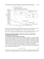
Thermophysical Properties of Bi-based High-Tc Superconductors
189
obtained by annealing the Fe-doped (Bi, Pb)
4
Sr
3
Ca
3
Cu
4-m
Fe
m
O
x
glassy precursor.
Phys. Rev. B. Vol. 58, No. 18, 12427–12432
Cloots, R., Bougrine, H., Houssa,M., Stassen, S., D’Urzo, L., Rulmont, A. & Ausloss, M.
(1994). Bi-based 2223 superconducting polycrystalline materials prepared by
either a solid state route or a glassy ‘matrix’ precursor method: Chemical analysis
as well as electrical and thermal transport properties. Physica C. Vol. 231, No. 3-
4, 259-270
Cohn, J.L., Skelton, E.F., Wolf, S.A., Liu, J.Z. & Shelton, R.N. (1992). Cyclotron resonance of
both magnetopolaron branches for polar and neutral optical phonon coupling in
the layer compound InSe.Phys. Rev. B vol. 45, No. 20, 12144-12147
Coskun, A., Ekicibil, A., Ozcelik, B. & Kyymaç, K. (2005). Effects of annealing time on the
magnetic properties of a Bi
1.7
Pb
0.29
Gd
0.01
Sr
2
Ca
3
Cu
4
O
12+ y
superconductor prepared
by the melt-quenching method. Chin. J. Phys. Vol. 43, No. 2, 372
Dey, T.K. (1998). Thermoelectric power of deoxygenated Bi
1.6
Pb
0.4
Sr
2
Ca
2
Cu
3
O
10+
sintered
superconducting pellets. J. Supercond. Vol.11, 367-372
Dorbolo, S., Ausloss, M., Bougrine, H., Robertz, B., Cloots, R., Mucha, J. & Durczewski, K.
(1999). Effect of synthesis process and substrate on electrical and thermal transport
properties of Bi-2212. J. Supercond. Vol. 12, Number 5, 623-629
Ekicibil, A., Coskun, A., Ozcelik, B. & Kyymacç, K. (2005). The magnetic and electrical
properties of rare earth Sm
3+
substituted Bi
1.7
Pb
0.3
Sr
2
Ca
2-x
Sm
x
Cu
3
O
12
system. Mod.
Phys. Lett. B Vol. 331, No. 6, 331-340
Gul, I.H., Rehman, M.A., Ali, M. & Maqsood, A. (2005). Effect of vanadium and barium on
the Bi-based (2223) superconductors. Physica C Vol. 432, No. 1-2, 71-80
Gusstafsson, S.E.(1991). Transient plane source techniques for thermal conductivity and
thermal diffusivity measurements of solid materials. Rev. Sci. Instrum. Vol. 62, No.
3, 797-804
Heremans, J., Morelli, D.T., Smith, G.W., Strite, S.C. (1988). Thermal and electronic
properties of rare-earth Ba
2
Cu
3
O
x
superconductors. Phys. Rev. B Vol. 37, 1604-
1610
Hirai, T.: In: Brook, R.J. (ed.) (1996). Processing of Ceramics, Part 2. VCH Verlagsgesellschaft
mbH, Weinheim
Hook, J.R., Hall, H.E. (1991). Solid State Phys, 2nd edn. Wiley, Chichester
Houssa, M. & Ausloos, M. (1995). Thermal conductivity of superconducting Bi
2
Sr
2
CaCu
2
O
8
and YBa
2
Cu
3
O
7-y.
Phys. Rev. B Vol. 51, No. 14, 9372-9374
Houssa, M. & Ausloos, M. (1996). n-plane electronic thermal conductivity of layered d-wave
high-T
c
superconductors. Physica C Vol. 257, No. 3-4, 321-331
Houssa,M., Ausloos,M. & Sergeenkov, S. (1996). The electronic contribution to the thermal
conductivity of layered high-T
c
materials. J. Phys.: Condens. Phys. Vol. 8, No. 12,
2043-2052
Hui, P.M., Zhang, X. ,Markworth, J. & Stroud, D. (1999). Thermal conductivity of graded
composites: Numerical simulations and an effective medium approximation. J.
Mater. Sci. Vol. 34, Number 22, 5497-5503
Applications of High-Tc Superconductivity
190
Ikebe, M. Fujisshiro, H. Naito, T., Noto, K. (1994). Simultaneous measurement of thermal
diffusivity and conductivity applied to Bi-2223ceramic superconductor. J. Phys. Soc.
Jpn. Vol. 63, 3107-3114
Jezowski, A., Mucha, J., Rogaci, K., Horyn, R., Bukovski, Z. & Horobiowski, M. (1987).
Thermal conductivity and electrical resistivity of the high-T
c
superconductor
YBa
2
Cu
3
O
9−Δ
. Phys. Lett. A Vol. 122, No. 8, 431-433
Khim, Z.G., Lee, S.C., Lee, J.H., Suh, B.J., Park, Y.W., Park, C., Yu, I.S. & Park, J.C. (1987).
Superconductivity in single-phase Y
1
Ba
2
Cu
3
O
9-x
and thermoelectric power
measurement. Phys. Rev. B Vol. 36, No. 4, 2305-2307
Knizek, K., Veverka, M., Hadova, E., Hejtmanek, J., Sedmidubsky, D. & Pollert, E.
(1998). Synthesis of HgBa
2
CuO
4+δ
by sol–gel method under controlled oxygen
pressure; electron and thermal transport properties. Physica C Vol. 302, No. 4,
290-298
Lee, S.C., Lee, J.H., Suh, B.J., Moon, S.H., Lim, C.J. & Khim, Z.G. (1988). Thermoelectric
power and superconducting properties of Y
1
Ba
2
Cu
3
O
7-δ
andR
1
Ba
2
Cu
3
O
7-δ.
Phys. Rev.
B Vol. 37, No. 4, 2285-2288
Lim, Z.S., Han, K.H., Salk, S.H. & Song, Y.S. (1989). Charged-particle interaction with
liquids: ripplon excitations. Phys. Rev. B Vol. 40, No. 1, 10-19
Mandal, J.B., Keshri, S., Mandal, P., Poddar, A., Das, A.N. & Ghosh, B. (1992).
Thermoelectric power of the Bi
2
Sr
2
Ca
1-x
Y
x
Cu
2
O
8+y
(x=0–1.0) system. Phys. Rev. B
Vol. 46, No. 18, 11840-11846
Maqsood A., Mahmood M.S., Suleman B. & Tasneem A. (1989). Preparation and
characterization of superconducting Dy
1
Ba
2
Cu
3
O
7−
x material. J. Mat. Sci. Lett. Vol.
8, No. 7, 757-758
Mitra, N. & Trefny, J. (1988). Thermoelectric power of the Tl-Ca-Ba-Cu-O superconductor.
Phys. Rev. B Vol. 38, No. 10, 7064-7066
Morelli, D.T., Heremans, J. & Swets, D.E. (1987). Thermal conductivity of superconductive
Y-Ba-Cu-O. Phys. Rev. B Vol. 36, No. 7, 3917-3919
Munakata, F., Matsuura, K., Kubo, K., Kawano, T. & Yamauchi, H. (1992). Thermoelectric
power of Bi
2
Sr
2
Ca
1-x
Y
x
Cu
2
O
8+y.
Phys. Rev. B Vol. 45, No. 18, 10604-10608
Nanda Kishore, K., Satyavathi, S., Muralidhar, A., Pena, O. & Hari Babu, V. (1995).
Thermoelectric power studies on the Sm substituted BPSCCO (2223)
superconductors. Physica C Vol. 252, No. 1-2, 49-53
Natividad, E., Castro, M., Burriel, R., Angurel, L.A., Diez, J.C. & Navarro, R. (2002).
Correlation of normal and superconducting transport properties on textured Bi-
2212 ceramic thin rods. Supercond. Sci. Technol. Vol. 15, No. 7, 1022
Ozhanli, Z., Yakýncý, M.E., Balcý, Y. & Aksan, M.A. (2002). Crystallization activation
energy and hole concentration properties of the Bi
2
Sr
2
Ca
1 − x
Cd
x
Cu
2
O
8 + y
glass-
ceramic superconductor Rods. J. Supercond. Vol. 15, No. 6, 543-547
Peacor, S.D., Cohn, J.L. & Uher, C. (1991). Effect of magnetic field on thermal conductivity
of YBa
2
Cu
3
O
7-δ
single crystals. Phys. Rev. B Vol. 43, No. 10, 8721-8724
Pinksi, F.J., Allen, P.B. & Butler, W.H. (1981). Calculated electrical and thermal resistivities
of Nb and Pd. Phys. Rev. B Vol. No. 10,23, 5080-5096
Thermophysical Properties of Bi-based High-Tc Superconductors
191
Rao, C.N.R., Ramakrishnan, T.V. & Kumar, N. (1990). Systematics in the thermopower
behaviour of several series of bismuth and thallium cuprate superconductors: An
interpretation of the temperature variation and the sign of the thermopower.
Physica C Vol. 165, No. 2, 183-188
Rehman, M.A. & Maqsood, A. (2005). Study of the thermal behaviour of Bi(Pb)Sr(Ba)-2223
high-T
c
granular superconductors. Physica C. Vol. 418, No. 3-4, 121-130
Rehman M.A. (2009). Thermal and electrothermal characterization of bismuth based high-
T
c
superconductors J. Alloys Comp. Vol. 469, No. 1-2, 66-72
Sera,M., Tanaka, S., Sato,M. & Fujishita, H. (1992). Anomalous thermoelectric power of
Bi
1.6
Pb
0.5
Sr
1.9−y
La
y
Cu
1.05
O
z
. Solid State Commun. Vol. 81, No. 5, 415-417
Suleiman, B.M., Haq, I., Karawacki, E.,Maqsood, A. & Gustafsson, S.E. (1993). Thermal
conductivity and electrical resistivity of the Y- and Er-substituted 1:2:3
superconducting compounds in the vicinity of the transition temperature. Phys.
Rev. B Vol. 48, No. 6, 4095-4102
Tewordt, L. (1963). Theory of the intrinsic electronic thermal conductivity of
superconductors Phys. Rev. Vol. 129, No.2, 657-663
Tewordt, L. & Wolkhausen, T. (1989). Theory of thermal conductivity of the lattice for high-
T
c
superconductors. Solid State Commun. Vol. 70, No. 8, 839-844
Tewordt, L. & Wolkhausen, T. (1990). Theory of phonon thermal conductivity for strong-
coupling s- and d-wave pairing in high T
c
superconductors. Solid State Commun.
Vol. 75, No. 6, 515-519
Uher, C. & Kaiser, A.B. (1987). Thermal transport properties of YBa
2
Cu
3
O
7
superconductors.
Phys. Rev. B Vol. 36, No. 10, 5680
Uher, C. & Wang, W.N. (1989). Thermoelectric power and thermal conductivity of neutron-
irradiated YBa
2
Cu
3
O
7-δ,
Phys. Rev. B Vol. 40, No. 4, 2694-2697
Uher, C.: In: Ginsberg, D.M. (ed.) Physical Properties of HTSC,vol. 3. World Scientific,
Singapore (1992)
Vasudeva R. V., Rangarajan, G. & Srinivasan, R. (1984). Thermoelectric power in the normal
state of Chevrel-phase superconductors of the type Cu
1.8
Mo
6
S
8-y
Se
y
, 0≤y≤8, and
Cu
1.8
Mo
6
S
8-y
Te
y
0≤y≤4. J Phys.F Vol.14, 973-980
Varoy, C.R., Trodahl, H.J., Buckley, R.G. & Kaiser, A.B. (1992). Thermopower of
Bi
2-x
Pb
x
Sr
2
CaCu
2
O
8+δ
. Phys. Rev. B Vol. 46, No. 1, 463-468
Yan, S., Lu, P. & Li, Q. (1988). Thermoelectric power of single phase YBa
2
Cu
3
O
7−x
superconductors. Solid State Commun. Vol. 65, No. 5, 355-358
Yu, R.C., Salamon, M.B., Lu, J.P. & Lee, W.C. (1992). Thermal conductivity of an
untwinned YBa
2
Cu
3
O
7-δ
single crystal and a new interpretation of the
superconducting state thermal transport. Phys. Rev. Lett. Vol. 69, No. 9, 1431-
1434
Varoy, C.R., Trodahl, H.J., Buckley, R.G. & Kaiser, A.B. (1992). Thermopower of Bi
2-
x
Pb
x
Sr
2
CaCu
2
O
8+δ.
Phys. Rev. B Vol. 46, No. 1, 463-468
Wang, J., Wakata, M., Kaneko, T., Takano, S. & Ya-mauchi, H.(1993). Enhancement of T
c
in
(Bi,Pb)-2223 superconductor by vacuum encapsulation and post-annealing. Physica
C vol. 208, No. 3-4, 323-327
Applications of High-Tc Superconductivity
192
Wermbter, S. & Tewordt, L. (1991). Theory of thermal conductivity and nuclear
relaxation rate for high temperature superconductors. Physica C Vol. 183, No.
4-6, 365-371
Wu M.K., Ashburn J.R., Torng C.J. & Horetal P.H. (1987). Superconductivity at 93 K in a
new mixed-phase Y-Ba-Cu-O compound system at ambient pressure. Phys. Rev.
Lett. Vol. 58, No. 9, 908-910
Ziman, J.M.: Electrons and Phonons. Clarendon, Oxford (1963)
9
Chemical Solution Deposition Based Oxide
Buffers and YBCO Coated Conductors
M. Parans Paranthaman
Chemical Sciences Division
Oak Ridge National Laboratory
USA
1. Introduction
The main objective of this work is to conduct fundamental research in the broad areas of
chemical solution based buffer and high temperature superconductor, namely Yttrium Barium
Copper Oxide (YBCO) development. The results of this research provide new insights in
buffer/superconductor areas and suggest methods to improve buffer/superconductor multi-
layer thin film fabrication. The overall purpose is to develop a potentially lower-cost, high
throughput, high yield, manufacturing processes for buffer/superconductor thin multi-layer
film fabrication, and to gain fundamental understanding of the growth of solution
buffer/superconductor layers for Rolling Assisted Biaxially Textured Substrate (RABiTS)
templates. This understanding is critical to the development of a reliable, robust, long-length
manufacturing process of second-generation (2G) wires for electric-power applications. In
order to reduce the cost of superconductor wires, it is necessary to replace the existing physical
vapor deposited three buffer layer RABiTS architecture of Yttrium Oxide, Y
2
O
3
seed/Yttria
Stabilized Zirconia, YSZ barrier/Cerium Oxide, CeO
2
cap with buffers deposited by
industrially scalable methods, such as slot-die coating of chemical solution deposition (CSD)
precursors [1-11]. Spin-coating is typically used to deposit short samples for optimizing the
CSD film growth conditions. In a typical chemical solution process, metal organic precursors
in suitable solvents are spin/dip/slot-die coated on either single crystal or biaxially textured
substrates followed by heat-treating in a tube furnace under controlled conditions. Chemical
Solution Deposition (CSD) process offers significant cost advantages compared to physical
vapor deposition (PVD) processes [5-11]. Solution coating is amenable to complex oxides, and
the materials utilization (yield) is almost 100%. The high-temperature superconductors (HTS)
such as (Bi,Pb)
2
Sr
2
Ca
2
Cu
3
O
10
(BSCCO or 2223 with a critical temperature, T
c
of 110 K) and
YBa
2
Cu
3
O
7-
δ
(YBCO or 123 with a T
c
of 91 K) have emerged as the leading candidate materials
for the first generation (1G) and second generation (2G) high temperature superconductor
wires or tapes that will carry high critical current density in liquid nitrogen temperatures [1,2].
Here, we report the growth of buffer/YBCO superconductor film growth using a chemical
solution method towards fabrication of second generation superconductor wires.
2. Chemical solution deposition of oxide buffers
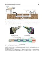
The schematic of the standard RABiTS architecture developed by Oak Ridge National
Laboratory and American Superconductor Corporation [3,4] is shown in Figure 1. The main
Applications of High-Tc Superconductivity
194
goal is to replace the most commonly used RABiTS architectures with a starting template of
biaxially textured Ni-5 at.% W substrate with a physical vapor deposited (PVD) seed layer
Fig. 1. The schematic of the standard RABiTS architecture.
Table 1. Structure, lattice misfit data and chemical solution deposition (CSD) methods for
various buffer layers. The lattice parameters were obtained from the International Center
for Diffraction Data, Powder Diffraction Files. ∗ Rhombohedral; ♦ Orthorhombic
Ni-5W
PVD-Y
2
O
3
seed
PVD-YSZ barrier
PVD-CeO
2
cap
CSD-YBCO
Standard
RABiTS Architecture
Ni-5W
seed
barrier
cap
CSD-YBCO
Replace ≥ 1 layer
b
y
CSD
Chemical Solution Deposition Based Oxide Buffers and YBCO Coated Conductors
195
of Y
2
O
3
, a barrier layer of YSZ, and a CeO
2
cap layer by a chemical solution deposition
method. To develop an all solution buffer/YBCO, it is necessary to either replace all three
layers or reduce the number of buffer layers to one. The role of the Y
2
O
3
seed layer is to
improve the out-of-plane texture of buffer layer compared to the underlying Ni-5W
substrate and Y
2
O
3
is also an excellent W diffusion and good oxygen barrier [4]. The role of
YSZ barrier layer is to contain the diffusion of Ni from the substrate into superconductor. In
order to grow YBCO superconductor films with critical current densities, it is necessary to
contain the poisoning of Ni into YBCO. Finally, the CeO
2
cap layer is compatible with CSD
based REBCO films and has enabled high critical current density REBCO films. The
optimized film thickness for each buffer layer is 75 nm and the typical YBCO layer thickness
is ~ 1 µm carrying a critical current of 250-300 A/cm-width at 77 K and self-field.
Researchers all over the world have developed several chemical solution deposited oxide
buffer layers that are suitable for YBCO film growth. A partial list of several epitaxial oxide
buffers grown using a CSD method have been reported in Table 1 [4]. It is possible for us to
select a buffer layer to lattice match with either the substrate Ni/Ni-W or with YBCO. The
list of chemical solution deposited buffer layers with YBCO superconductor films deposited
on such buffers is reported in Table 2.
CSD Buffer
Layers
Stacking for YBCO
J
c
(MA/cm
2
)
Reference
CeO
2
YBCO (CSD)/CeO
2
(Sputtered)/YSZ
(Sputtered)/CeO
2
(CSD)/Ni-W
3.3 39
YSZ YBCO (CSD)/CeO
2
(CSD)/YSZ (CSD)/
CeO
2
(CSD)/Ni
0.5 35
Y
2
O
3
YBCO (PLD)/CeO
2
(Sputtered)/YSZ
(Sputtered)/Y
2
O
3
(CSD)/Ni-W
1.2 31
Eu
2
O
3
YBCO (ex-situ BaF
2
)/CeO
2
(Sputtered)/
YSZ (Sputtered)/Eu
2
O
3
(CSD)/Ni
1.1 20
Gd
2
O
3
YBCO (PLD)/CeO
2
(Sputtered)/YSZ
(Sputtered)/Gd
2
O
3
(CSD)/Ni-W-Fe
1 36
Ce-Gd-O YBCO (CSD)/CeO
2
(CSD)/CGO (CSD)/
Gd
2
O
3
(CSD)/Ni
0.1 37
SrTiO
3
YBCO (CSD)/STO (CSD)/Ni 1.3 38
La
2
Zr
2
O
7
YBCO (e-beam)/CeO
2
(Sputtered)/YSZ
(Sputtered)/LZO (CSD)/Ni
0.48 26
La
1/4
Zr
3/4
O
y
YBCO (PLD)/La
1/4
Zr
3/4
O
y
(CSD)/Ni-W 0.55 42
Gd
2
Zr
2
O
7
YBCO (MOCVD)/GZO (CSD)/Ni 1.3 33
Gd
3
NbO
7
YBCO (PLD)/GNO (CSD)/Ni-W 1.1 30
Table 2. List of chemical solution deposited oxide buffer layers with J
c
of the high
temperature superconducting YBCO films deposited on such buffers.
Applications of High-Tc Superconductivity
196
3. Chemical solution deposition of REBCO
Currently, chemical solution based synthesis of YBCO uses a trifluoroacetate (TFA) based
precursor approach [5]. In this approach, the precursor solution is prepared by dissolving
Yttrium, Barium and Copper trifluoroacetates in methanol. Then the precursor solution is
spin/slot-die coated on RABiTS templates followed a two-stage heat-treatment to convert
the precursor films to high quality YBCO. In the first stage (pyrolysis), there is a significant
bottle neck to processing rates for these films because the shrinkage stresses developed in
the films during pyrolysis need to be accommodated using very slow heating rates. The
reactions taking place during the synthesis are illustrated below:
Y(OOCCF
3
)
3
+ 2 Ba(OOCCF
3
)
2
+ 3 Cu(OOCCF
3
)
3
0.5 Y
2
O
3
+ 2 BaF
2
+ 3 CuO + (nCO
2
+ mC
x
O
y
F
2
) (1)
0.5 Y
2
O
3
+ 2 BaF
2
+ 3 CuO +2 H
2
O YBa
2
Cu
3
O
7-
δ
+ 4HF (2)
Significant efforts were made to increase the growth rate by replacing part of the metal TFA
precursors with non-fluorine based precursors and also adjust the water and oxygen
pressure during the growth of YBCO films. Another advantage of the TFA process is to
introduce mixed rare earths and Zirconium oxides into the starting precursors to enhance
the flux-pinning properties of REBCO films [5,40,41]. Chemical solution deposition method
may prove to be a promising route for producing a low-cost all-CSD buffer/YBCO based
coated conductors. The main challenge is to fabricate high-temperature superconductor
tapes in kilometer lengths in carrying 1000 A/cm-width. Industries from US and Japan are
leading in this area while industries from Europe, Korea, and China are only few years
away.
4. Summary
In summary, RABiTS template with several possible architectures based on chemical
solution deposition methods have been developed and superconductivity industries around
the world are in the process of taking the technology to the pilot scale to produce
commercially acceptable 500 meter lengths. The research in the area of second generation
high temperature superconductor wire technology to increase the flux pinning properties of
YBCO superconductor and to reduce the ac loss in these wires for various electric-power
applications such as transmission cables, fault-current limiters and high-field magnets is
continuing ahead.
5. Acknowledgements
This work was supported by the U.S. Department of Energy, Office of Electricity Delivery
and Energy Reliability (OE) – Advanced Conductors and Cables Program.
6. References
[1] M. Parans Paranthaman and T. Izumi, Editors, “High-Performance YBCO-Coated
Superconductor Wires,” MRS Bulletin 29 (2004) 533-536.
Chemical Solution Deposition Based Oxide Buffers and YBCO Coated Conductors
197
[2] M. Parans Paranthaman, “Superconductor Wires,” in McGraw-Hill 2006 Yearbook of
Science and Technology, McGraw-Hill Publishers, New York (2006) pp. 319-322.
[3] A. Goyal, D.P. Norton, J.D. Budai, M. Paranthaman, E.D. Specht, D.M. Kroeger, D.K.
Christen, Q. He, B. Saffian, F.A. List, D.F. Lee, P.M. Martin, C.E. Klabunde, E.
Hatfield, V.K. Sikka, “Fabrication of Long Range, Biaxially Textured, High
Temperature Superconducting Tape on Rolled Ni Substrates,”
Appl. Phys. Lett. 69
(1996) 1795.
[4] A. Goyal, M. Paranthaman, and U. Schoop, “The RABiTS Approach: Using Rolling-
Assisted Biaxially Textured Substrates for High-Performance YBCO
Superconductors,”
MRS Bulletin 29 (2004) 552-561.
[5] M.W. Rupich, D.T. Verebelyi, W. Zhang, T. Kodenkandath, and X. Li, Metalorganic
Deposition of YBCO Films for Second-Generation High-Temperature
Superconductor Wires,” MRS Bulletin 29 (2004) 572-578.
[6] C.J. Brinker, A.J. Hurd, P.R. Schunk, G.C. Frye, C.S. Ashley, “Review of Sol-gel Thin
Film Formation,” J. Non-Cryst. Solids 147 (1992) 424.
[7] F.F. Lange, “Chemical Solution Routes to Single-crystal Thin Films,” Science 273 (1996)
903.
[8] R.W. Schwartz, “Chemical Solution Deposition of Perovskite Thin Films,” Chem. Mater.
9 (1997) 2325.
[9] S. Sathyamurthy, M. Paranthaman, Lee Heatherly, Patrick M. Martin, E.D. Specht, Amit
Goyal, Thomas Kodenkandath, Xiaoping Li, Martin W. Rupich, “Solution-
processed lanthanum zirconium oxide as a barrier layer for high I
c
coated
conductors,”
J. Mater. Res. 21 (2006) 910.
[10] M.P. Paranthaman, S. Sathyamurthy, M.S. Bhuiyan, P.M. Martin, T. Aytug, K. Kim, M.
Fayek, K.J. Leonard, J. Li, A. Goyal, T. Kodenkandath, X. Li, W. Zhang, M.W.
Rupich, “MOD buffer/YBCO approach to fabricate low-cost second generation
HTS wires,”
IEEE Trans. On Appl. Supercond. 17 (2007) 3332.
[11] M. Coll, J. Gazquez, R. Huhne, B. Holzapfel, Y. Morilla, J. Garcia-Lopez, A. Pomar, F.
Sandiumenge, T. Puig, X. Obradors, “All chemical YBa
2
Cu
3
O
7
superconducting
multilayers: Critical role of CeO
2
cap layer flatness,” J. Mater. Res. 24 (2009) 1446.
[12] G.N. Glavee, R.D. Hunt and M. Paranthaman, “Low Temperature Preparation of
BaCeO
3
and Ce
0.75
Zr
0.25
O
2
Thin Films Using Sol-gel Processing Techniques,”
Materials Research Bulletin 34 (1999) 817-825.
[13] M. Paranthaman, S.S. Shoup, D.B. Beach, R.K. Williams and E.D. Specht, “Epitaxial
Growth of BaZrO
3
Films on Single Crystal Oxide Substrates Using Sol-gel Alkoxide
Precursors,”
Materials Research Bulletin 32 (1997) 1697-1704.
[14] N.J. Ali, P. Clem and S.J. Milne, “Synthesis of sols for the production of La- modified
PbTiO
3
thin films,” J. Mater. Sci. Lett. 14 (1995) 837-840.
[15] M. P. Paranthaman, M. S. Bhuiyan, S. Sathyamurthy, L. Heatherly, C. Cantoni and A.
Goyal, “Improved textured La
2
Zr
2
O
7
buffer on La
3
TaO
7
seed for all-MOD
Buffer/YBCO coated conductors,”
Physica C 468 (2008) 1587.
[16] M.S. Bhuiyan, M. Paranthaman, S. Sathyamurthy, “Chemical solution-based epitaxial
oxide films on biaxially textured Ni-W substrates with improved out-of-plane
texture for YBCO coated conductors,”
J. Electronic Mater. 36 (2007) 1270.
Applications of High-Tc Superconductivity
198
[17] M.S. Bhuiyan, M. Paranthaman, A. Goyal, L. Heatherly and D.B. Beach, “Deposition of
rare earth tantalite buffers on textured Ni-W substrates for YBCO coated conductor
using chemical solution deposition approach,” J. Mater. Res. 21 (2006) 767-773.
[18] J.T. Dawley, R.J. Ong and P.G. Clem, “Improving sol-gel YBa
2
Cu
3
O
7-
δ
film morphology
using high-boiling-point solvents,” J. Mater. Res. 17 (2002) 1678-1685.
[19] S. Sathyamurthy and K. Salama, “Application of metal–organic decomposition
techniques for the deposition of buffer layers and Y123 for coated-conductor
fabrication,” Physica C 329 (2000) 58-68.
[20] M. Paranthaman, T.G. Chirayil, F.A. List, X. Cui, A. Goyal, D.F. Lee, E.D. Specht, P.M.
Martin, R.K. Williams, D.M. Kroeger, J.S. Morrell, D.B. Beach, R. Feenstra and D.K.
Christen, “Fabrication of Long Lengths of Epitaxial Buffer Layers on Biaxially
Textured-Ni Substrates using a Continuous Reel-to-reel Dip-coating Unit,”
J. Amer.
Ceram. Soc. 84 (2001) 273-278.
[21] Y. Akin, Z.K. Heiba, W. Sigmund and Y.S. Hascicek, “Engineered oxide thin films as
100% lattice match buffer layers for YBCO coated conductors,” Solid-State
Electronics 47 (2003) 2171-2175.
[22] C.Y. Yang, A. Ichinose, S.E. Babcock, J.S. Morrell, J.E. Mathis, D.T. Verebelyi, M.
Paranthaman, D.B. Beach and D.K. Christen, “Microstructure of a High J
c
Laser-
ablated YBa
2
Cu
3
O
7-
δ
/Sol-gel Deposited NdGaO
3
Buffer Layer/(001) SrTiO
3
Multi-
layer Structure,”
Physica C 331 (2000) 73-78.
[23] M.S. Bhuiyan, M. Paranthaman, S. Sathyamurthy, T. Aytug, S. Kang, D. F. Lee, A.
Goyal, E. A. Payzant, and K. Salama, “MOD approach for the growth of epitaxial
CeO
2
buffer layers on biaxially textured Ni-W substrates for YBCO coated
conductors,” Superconductor Science & Technology 16 (2003) 1305-1309.
[24] J.S. Morrell, Z.B. Xue, E.D. Specht, A. Goyal, P.M. Martin, D.F. Lee, R. Feenstra, D.T.
Verebelyi, D.K. Christen, T.G. Chirayil, M. Paranthaman, C.E. Vallet and D.B.
Beach, “Epitaxial Growth of Gadolinium Oxide on Roll-Textured Nickel Using a
Solution Growth Technique,”
J. Mater. Res. 15 (2000) 621-628.
[25] T.G. Chirayil, M. Paranthaman, D.B. Beach, D.F. Lee, A. Goyal, R.K. Williams, X. Cui,
D.M. Kroeger, R. Feenstra, D.T. Verebelyi, and D.K. Christen, “Epitaxial growth of
La
2
Zr
2
O
7
thin films on rolled Ni-substrates by sol–gel process for high T
c
superconducting tapes,” Physica C 336 (2000) 63-69.
[26] S. Sathyamurthy, M. Paranthaman, H.Y. Zhai, H.M. Christen, P.M. Martin and A.
Goyal, “Lanthanum zirconate: A single buffer layer processed by solution
deposition for coated conductor fabrication,”
J. Mater. Res. 17 (2002) 2181-2184.
[27] M. Parans Paranthaman, T. Aytug, S. Sathyamurthy, D.B. Beach, A. Golyal, D.F. Lee,
B.W. Kang, L. Heatherly, E.D. Specht, K.J. Leonard et al., “Bulk Solution
Techniques to Fabricate High Jc YBCO Coated Conductors,”
Physica C 378-381
(2002) 1009-1012.
[28] S. S. Shoup, M. Paranthaman, A. Goyal, E. D. Specht, D. F. Lee, D. M. Kroeger and D.
B. Beach, “Epitaxial Thin Film Growth of Lanthanum and Neodymium Aluminate
Films on Roll-Textured Nickel Using a Sol-Gel Method,” J. Amer. Ceram. Soc. 81
(1998) 3019-3021.
Chemical Solution Deposition Based Oxide Buffers and YBCO Coated Conductors
199
[29] M.W. Rupich, W. Palm, W. Zhang, E. Siegal, S. Annavarapu, L. Fritzemeier, M.D.
Teplitsky, C. Thieme and M. Paranthaman, “Growth and Characterization of Oxide
Buffer Layers for YBCO Coated Conductors,”
IEEE Trans. on Appl. Supercond. 9
(1999) 1527-1530.
[30] M. Paranthaman, M.S. Bhuiyan, S. Sathyamurthy, H.Y. Zhai, A. Goyal and K. Salama,
“Epitaxial Growth of Solution Based Rare Earth Niobate, RE
3
NbO
7
Films on
Biaxially Textured Ni-W Substrates,”
J. Mater. Res. 20 (2005) 6-9.
[31] M.S. Bhuiyan, M. Paranthaman, S. Kang, D.F. Lee, and K. Salama, “Growth of epitaxial
Y
2
O
3
buffer layers on biaxially textured Ni-W substrates for YBCO coated
conductors by MOD approach,” Physica C 422 (2005) 95-101.
[32] T. Aytug, M. Paranthaman, K.J. Leonard, H.Y. Zhai, M.S. Bhuiyan, E.A. Payzant, A.
Goyal, S. Sathyamurthy, D.B. Beach, P.M. Martin, D.K. Christen, X. Li, T.
Kodenkandath, U. Schoop, M.W. Rupich, H.E. Smith, T. Haugan, P.N. Barnes,
“Assessment of chemical solution synthesis and properties of Gd
2
Zr
2
O
7
thin films
as buffer layers for second-generation high-temperature superconductor wires”
J.
Mater. Res. 20 (2005) 2988-2996.
[33] Y.X. Zhou, X. Zhang, H. Fang, R.T. Putman and K. Salama, “Development of Single
Solution Buffer Layers on Textured Ni Substrate for HTS Coated Conductors,”
IEEE Trans. On Appl. Supercond. 15 (2005) 2711-2714.
[34] T.G. Chirayil, M. Paranthaman, D.B. Beach, J.S. Morrell, E.Y. Sun, A. Goyal, R.K.
Williams, D.F. Lee, P.M. Martin, D.M. Kroeger, R. Feenstra, D.T. Verebelyi and
D.K. Christen, “Epitaxial Growth of Yb
2
O
3
Buffer Layers on Biaxially Textured-Ni
(100) substrates by Sol-gel Process,” Mat. Res. Soc. Symp. Proc. (1999) 51-56.
[35] Y. Akin, Z. Aslanoglu, E. Celik, L. Arda, W. Sigmund and Y.S. Hascicek, “Textured
Growth of Multi-Layered Buffer Layers on Ni tape by Sol-Gel Process,” IEEE
Trans. Appl. Supercond. 13 (2003) 2673.
[36] T. Aytug, M.P. Paranthaman, B.W. Kang, D.B. Beach, S. Sathyamurthy, E.D. Specht,
D.F. Lee, R. Feenstra, A. Goyal, D.M. Kroeger, K.J. Leonard, P.M. Martin and D.K.
Christen, “Reel-to-reel continuous chemical solution deposition of epitaxial Gd
2
O
3
buffer layers on biaxially textured metal tapes for the fabrication of YBa
2
Cu
3
O
7-
δ
coated conductors,” Journal of The American Ceramic Society 86 (2003) 257-265.
[37] Y. Takahashi, Y. Aoki, T. Hasegawa, T. Watanabe, T. Maeda, T. Honjo and Y. Shiohara,
“In-plane textured buffer layer for the TFA-MOD method on <100>{001} Ni tapes
using MOD process,” Physica C 392–396 (2003) 887.
[38] M.P. Siegal, P.G. Clem, J.T. Dawley, R.J. Ong, M. A. Rodriguez and D.L. Overmyer,
“All solution-chemistry approach for YBa
2
Cu
3
O
7-
δ
coated conductors,” Appl. Phys.
Lett. 80 (2002) 2710.
[39] M. P. Paranthaman, X. Qiu, K. Kim, Y. Zhang, X. Li, S. Sathyamurthy, C. Thieme, and
M. W. Rupich, “Development of Solution Buffer Layers for RABiTS Based YBCO
Coated Conductors,”
IEEE Trans. On Appl. Supercond. (2011) in press.
[40] Y Shiohara, M Yoshizumi, T Izumi and Y Yamada, “Present status and future prospect
of coated conductor development and its application in Japan,” Superconductor
Science and Technology 21 (2008) 034002.
Applications of High-Tc Superconductivity
200
[41] J. Gutiérrez, A. Llordés, J. Gazquez, M. Gibert, N. Romá, S. Ricart, A. Pomar, F.
Sandiumenge, N. Mestres, T. Puig and X. Obradors, “Strong isotropic flux pinning
in solution-derived YBa
2
Cu
3
O
7−x
nanocomposite superconductor films,” Nature
Materials 6 (2007) 367‐373.
[42] M. P. Paranthaman, S. Sathyamurthy, X. P. Li, E. D. Specht, S. H. Wee, C. Cantoni, A.
Goyal, and M. W. Rupich, “Modified Lanthanum Zirconium Oxide buffer layers
for low-cost, high performance YBCO coated conductors,” Physica C 470 (2010)
352.
10
Superconducting Properties of
Graphene Doped Magnesium Diboride
Xun Xu, Wenxian Li, Xiaolin Wang and Shi-Xue Dou
University of Wollongong/ Institute for Superconducting and Electronic Materials
Australia
1. Introduction
Graphene, carbon in the form of monolayer sheets, has revealed astonishing and unique
chemical and physical properties, which have made it an extremely active research topic in
both materials science and physics (Novoselov, K. S. et al., 2004). Through chemical and
materials integration, graphene is being actively exploited in a range of technological
applications (Stankovich, S. et al., 2006). Superconductors can carry electrical current
without any energy dissipation. The combination of both graphene and a superconductor
into a composite has great potential for electrical devices and large scale applications. MgB
2
,
a superconductor with a simple composition and two-gap feature has great potential for
large current carrying applications, as demonstrated through a series of chemical dopings
(Dou, S. X. et al. 2007). In the case of graphene’s, the strict two-dimensionality and its high
electrical and thermal conductivities, make it an ideal candidate for integrating/doping into
MgB
2
in order to improve the superconducting properties.
Substitutional chemistry can modify, in a controlled way, the electronic structures of
superconductors and their superconducting properties, such as the transition temperature
(T
c
), critical current density (J
c
), upper critical field (H
c2
), and irreversibility field (H
irr
). In
particular, carbon containing dopants, including nano-meter sized carbon (nano-C), silicon
carbide (SiC), carbon nanotubes (CNTs) and hydrocarbons/carbohydrates are effective
means to enhance the J
c
- field dependence and H
c2
(Ma, Y. et al., 2006, Senlowocz, B. J. et al.,
2005, Kumakura, H. et al., 2004, Sumption, M. et al., 2005, Dou, S. X. et al., 2003, Kim, J. H. et
al., 2006, Wilke, R. H. T. et al., 2008). Upon graphene incorporation into MgB
2
it is expected
that H
c2
and the flux pinning properties should be improved. Recently, high-throughput
solution processing of large-scale graphene has been reported by a number of groups (Tung,
V. C. et al., 2009, Kim, K. S. et al., 2009, Hernandez, Y. et al., 2008, Li, D. et al., 2008, Li, X. et
al., 2008, Choucair, M. et al., 2009).
Based on the works of Choucair et al., sufficient quantities of graphene were obtained for
doping the bulk MgB
2
samples via a diffusion process. it was demonstrate that graphene
is the most efficient among all the carbon-based dopants used to date, in terms of
enhancing the flux pinning behaviour in MgB
2
. Very low levels of graphene doping (e,g.
0.9 at%) have been shown to be sufficient to lead to a significant improvement in the
critical current density - field performance (J
c
(B)), with little change in the transition
temperature (T
c
). At 3.7 at% graphene doping of MgB
2
an optimal enhancement in J
c
(B)
was reached by a factor of 30 at 5 K and 10 T, compared to the un-doped reference
Applications of High-Tc Superconductivity
202
sample. This improvement is believed to be related to: the single carbon sheet two
dimensional (2-D) geometry, the negative thermal expansion coefficient, high electron
mobility, low resistivity, high thermal conductivity, and high mechanical strength of
graphene. In contrast to many carbon-based dopants, where carbon substitution and
hence scattering, is the dominant factor for enhancement of J
c
(B), the enhanced flux
pinning is largely attributable to strong strain effects induced by the large difference
between the negative coefficient of thermal expansion of graphene and the large,
anisotropic coefficient of thermal expansion of MgB
2
.
Fig. 1. Crystal structure of MgB
2
, a=3.086 Å and c=3.524 Å (Nagamatsu, J. et al., 2001).
The most exciting result is the soften E
2g
mode in graphene added samples. It is well known
that the superconductivity of intermetallic compound MgB
2
is self-optimized both in
electronic structure and in phonon dispersion and slim chance is left to improve its
superconducting transition temperature, T
c
, above ~39.4 K (Nagamatsu, J. et al., 2001).
Higher T
c
of Mg
10
B
2
and band structure calculation indicate that MgB
2
is a phonon-mediated
BCS-Eliashberg superconductor with multiple gaps and strong electron-phonon coupling
(EPC). As a two-gap superconductor, MgB
2
shows two qualitatively different Fermi
surfaces: σ-band with extremely strong pairing strength and π-band with weak pairing
strength. The σ-band contribution is dominant and specifically the contribution from its
coupling with the B-B stretch modes with E
2g
symmetry in boron layer, the only Raman
active phonon modes according to first principle calculation (Kunc, K. et al, 2001). the T
c
does not show improvements in the alloys due to carbon substitution and impurity
scattering, a tensile strain effects assuredly exist in the alloys judging from both the width of
superconducting energy gaps and the phonon behaviors.
2. Graphene doped polycrystalline MgB
2
MgB
2
is an intermetallic, polycrystalline material that had been known since 1953 and was
used in the commercial preparation of elemental boron (B). It was not known to be
superconducting until this property was accidentally discovered by Jun Akimitsu and his
colleagues (Nagamatsu, J. et al., 2001). MgB
2
consists of alternating layers of boron and
magnesium atoms in a hexagonal structure, as shown in Figure 1. It was analyzed that the
crystal structure of MgB
2
using by the Rietveld method . It was found that the compound
has hexagonal symmetry (Space Group P6/mmm) with the unit cell lattice parameters: a =
Superconducting Properties of Graphene Doped Magnesium Diboride
203
0.3086 nm and c = 0.3524 nm. Similar conclusions on the crystal structure were soon made
on the basis of studies using high resolution transmission electron microscopy (HRTEM),
high resolution powder neutron diffraction and electron energy loss spectroscopy .
Up to now, large number of experimental and theoretical of works has been studied because
of its high T
c
of 39 K. Beside the high T
c
, simple crystal structure, large coherence length,
high critical field, transparency of grain boundaries, and low normal state resistivity are a
fascinating topic to study for both large scale application and electronic devices. Moreover,
the presence of two-gap superconductivity (π and σ band) has been theoretically and
experimentally established besides it shows a significant isotope effect like a low
temperature superconductor.
2.1 Dual reaction model and C doping effects in MgB
2
The “pure” MgB
2
is not so good for applications due to the poor flux pinning and low J
c
, H
c2
and H
irr
values. A significant enhancement of critical current density (J
c
) in MgB
2
can be
achieved through chemical doping with various kinds of material. Chemical doping is a
simple and readily scalable technique. A significant enhancement of critical current density (J
c
)
in MgB
2
can be achieved through chemical doping with carbon (C) containing composites or
compounds, such as SiC, C, B
4
C, or carbon nanotubes (CNT), hydrocarbon, carbohydrates etc.
The C can enter the MgB
2
structure by substituting into boron (B) sites, and thus J
c
and H
c2
are
significantly enhanced due to the increased impurity scattering in the two-band MgB
2
.
In 2007, Dou et al has proposed a dual reaction model based on the following factors to
explain the mechanism of enhancing the electromagnetic properties due to the SiC and C
doping (Dou, S. X. et al. 2007):
Demonstrated a dual reaction model in which the C substitution due to nano SiC
doping and MgB
2
formation take place simultaneously at temperatures
The C substitution and induced highly localised fluctuation in structure and T
c
are
responsible for the enhancement in J
c
, Hirr and Hc
2
by SiC doping.
Disorder created by all means has universal influence on electromagnetic properties of
MgB2
free and reactive C is the key to searching for better do pants
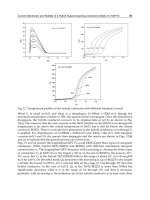
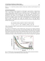
Fig. 2 shows the effects of sintering temperature on the J
c
(H) for different carbon based
dopants. The hydrocarbon and SiC doped MgB
2
show significant enhancement in J
c
for
the samples sintered at lower temperature, whereas the carbon and CNT doped MgB
2
need to be sintered at higher temperature for high J
c
. The low sintering temperature
results in small grain size, high concentrations of impurities and defects, and large
lattice distortion, which are all responsible for a strong flux pinning force (Soltanian et
al., 2005, Yamamoto et al., 2005). Furthermore, the hydrocarbon and SiC can release
fresh and active free carbon at very low temperature, which means that the carbon
substitution effects take place simultaneously with the MgB
2
formation. A high
sintering temperature will perfect the crystallization and decrease the flux pinning
centers in the MgB
2
matrix. That is the reason why high sintering temperature degrades
the J
c
performance. Although high sintering temperature has the same shortcomings in
nanosized carbon and CNT doped MgB
2
, the carbon substitution effects improve their J
c
values. The high sintering temperature is necessary for carbon and CNT doped MgB
2
because the carbon and CNT are quite stable at low temperature and the substitution
effects are absent if the sintering temperature is not high enough.
Applications of High-Tc Superconductivity
204
Fig. 2. The critical current density (J
c
) at 4.2 K versus magnetic field for wires of pure MgB
2
and MgB
2
doped with C, SiC, SWCNTs, and malic acid that were sintered at different
temperatures (Dou et al., 2002; Yeoh et al., 2006; Dou et al., 2007; Kim et al., 2008)
2.2 Gram-scale production of graphene
Graphite is the most common allotrope of carbon. The name isderived from the Greek verb
graphein, ‘to write’, which relates very literally to the compound we now know as graphene,
as single sheets of graphene were first isolated by simply tracing a sample of bulk graphite
across a substrate in a process known as micromechanical cleavage (Novoselov, K. S. et al.,
2004). Further attempts to synthesize isolated graphene have been based on intercalation (Li,
X. et al., 2008), sonication in various solvents (Hernandez, Y. et al., 2008) and the chemical
reduction of graphite to yield few-layer graphite oxide (Li, D. et al., 2008). Approaches
developed for the production of carbon nanotubes have also been explored, but so far they
have only been able to produce graphitic film (Dikin, D. A. et al., 2007). However, single- and
few-layer graphene sheets have been grown epitaxially by the chemical vapour deposition of
hydrocarbons on metal and nonmetal substrates, substrate-free deposition and by thermal
decomposition of SiC. Given the lack of a reliable top-down approach for the large-scale
production of graphene, attention has turned to bottom-up approaches that might be able to
deliver the economies of scale that are found in the chemical and pharmaceutical industries.
Choucair et al. have demonstrated that single-layer graphene can be synthesized by low-
temperature flash pyrolysis of a solvothermal product of sodium and ethanol, followed by
gentle sonication of the nanoporous carbon product (Choucair, M. et al., 2009).
All solvothermal reactions were performed in a Teflon-lined Parr Instrument Company 4749
reactor having a maximum volume of 23 ml. A typical synthesis consists of heating a 1:1
molar ratio of sodium (2 g) and ethanol (5 ml) in a sealed reactor vessel at 220°C for 72 h to
yield the solid solvothermal product—the graphene precursor. This material is then rapidly
pyrolysed, and the remaining product washed with deionized water (100 ml). The
suspended solid is then vacuum filtered and dried in a vacuum oven at 100°C for 24 h. The
final yield of graphene is approximately 0.1 g per 1 ml of ethanol—typically yielding ~0.5 g
Superconducting Properties of Graphene Doped Magnesium Diboride
205
Fig. 3. Example of the bulk quantity of graphene product. The image consists of
approximately 2 g of sample (Choucair, M. et al., 2009).
per solvothermal reaction.The product of this reaction is then washed in water and dried to
obtain pure graphene (Fig. 3). Solvothermal reactions have been reported to lead to the
production of carbon nanosheets, although such materials do not appear to consist of single
sheets having both high degrees of planarityand crystallinity, suggesting an amorphous or
disordered graphitic structure (Choucair, M. et al., 2009).
2.3 Graphene doping effects in MgB
2
Based on the works of Choucair et al., sufficient quantities of graphene were made
available for doping the bulk MgB
2
samples. The bulk MgB
2
samples were fabricated via a
diffusion process. The crystalline boron powder (0.2 to 2.4 µm) 99.999% without and with
graphene was prepared by ball milling with toluene medium. Then, the powders were
dried in a vacuum oven to evaporate the medium. These powders were mixed and
pressed into pellets. The pellets were then put into an iron tube filled with Mg powder (-
325mesh 99%). The samples were sintered at 850°C for 10 hrs in a quartz tube; the heating
rate was 5
o
Cmin
-1
under high purity argon (Ar 99.9%) gas. The phase and crystal structure
of all the samples were investigated by X-ray diffraction (XRD). T
c
was defined as the
onset temperature at which diamagnetic properties were observed. The magnetic J
c
was
derived from the width of the magnetization loop using Bean’s model by a Physical
Properties Measurement System (PPMS). Transport measurements for resistivity (ρ) were
done using a standard AC four probe method. In addition, H
c2
(T)
and H
irr
(T)
were defined
as the fields where the temperature dependent resistance at constant magnetic field R(H
c2
,
T) = 0.9R
ns
and R(H
irr
, T) = 0.1R
ns
with R
ns
being the normal state resistance near 40 K. The
hysteresis loops of the MgB
2
sample every 1.5 K in the 17- 35 K range. The symmetric
hysteresis loops with respect to the magnetic field indicate the dominance of bulk pinning
up to temperatures near T
c
.
MgB
2
/Fe monofilament wires were prepared by an in situ reaction process and the powder-
in-tube method. Magnesium (99%, 325 mesh), and the different boron powders with the
nominal atomic ratio of Mg : B = 1.1 : 2 were mixed through grinding and were put into Fe
Applications of High-Tc Superconductivity
206
tubes with a length of 140 mm, an outer diameter (O.D) of 10 mm, and an inner diameter
(I.D) of 8 mm. The packing process was carried out in air. Both ends of the tubes were sealed
with aluminum pieces, and then the tubes were drawn to a wire with a diameter of 1.4 mm.
Short wire samples (4 cm each) were sealed with Zr foil, then sintered with a heating rate of
5
o
C min
-1
in flowing high purity Ar to 700-800
o
C and held at the final temperature for 30
minutes, followed by a furnace cooling to room temperature. The transport current (I
c
) at 4.2
K was measured by the standard dc four-probe resistive method with a criterion of 1 μVcm
-1
in magnetic fields up to 12 T. T
c
was determined using the standard ac four-probe method.
In addition, H
c2
(T) and H
irr
(T) were defined as the fields where the temperature dependent
resistance at constant magnetic field R(H
c2
, T) = 0.9R
ns
and R(H
irr
,T) = 0.1R
ns
, respectively,
with R
ns
being the normal state resistance near 40 K.
The common format Mg(B
1-x
C
x
)
2
with x=0, 0.037, was used. The composition of graphene
doped MgB
2
were 0, 3.7 at%, and as such, the samples are designated as G000, and
G037respectively.
2.3.1 XRD analysis for bulk samples
Fig. 4 shows XRD patterns for the pure and graphene doped MgB
2
samples. All the peaks
are inherent to MgB
2.
No impurity phase was detected in the XRD data, however a slight
peak shift to higher angle is noted for the G087 samples. MgO, which is commonly present
in most bulk MgB
2
samples is absent in all the samples.
The lattice parameters, a, c, the ratio of a/c, grain size, strain, and full width at half
maximum of the representative peak (110) calculated from the XRD patterns are shown in
Table 1. Both the a-axis and c-axis parameters vary little with increasing graphene doping
level of 3.7%, apart from G087 sample, which shows a notable decrease in the a-axis
parameter, suggesting that carbon (C) likely substitutes into the boron (B) sites, leading to
a slight drop in T
c
(36.7 K) for the G087 sample. it also observed that the full width at half
maximum (FWHM) of the (110) peak increases with increasing graphene doping level.
Such a peak broadening is caused by both grain size reduction and an increase in lattice
strain. The calculated results on grain size and lattice strain from a Williamson-Hall plot
(Williamson, G. K., and Hall, W. H., 1953) are given in Table 1. Transition temperatures
(T
c
) for the graphene doped samples were determined by AC susceptibility
measurements. Also, the T
c
onset determined from the AC susceptibility measurement is
38.9 K for the un-doped sample, dropping only slightly to 37.7 and 36.7 K for the G037
and G087 samples, respectively.
Sample
Lattice Constants
Grain
Size
(nm)
Strain
(%)
FWHM
(110)
()
T
c
(onset)
(K)
a (Å) c (Å)
c/a
G000 3.084(1) 3.525(1) 1.143(1) 216(10) 0.1198(188) 0.288 38.9
G037 3.082(1) 3.527(1) 1.144(1) 170(8) 0.1685(250) 0.400 37.7
G087 3.075(1) 3.525(1) 1.146(1) 171(11) 0.1782(330) 0.414 36.7
Table 1. The full width at half maximum (FWHM) of the (110) peak, the lattice parameters,
and the transition temperature (T
c
) for the MgB
2
samples, made with 0, 3.7, and 8.7 at%
graphene doping via a diffusion process (Xu, X. et al., 2010).
Superconducting Properties of Graphene Doped Magnesium Diboride
207
Fig. 4. XRD patterns for graphene doped MgB
2
samples: G000, G009, G019, G037, and G087,
showing that all diffraction peaks can be indexed to MgB
2
with undetectable impurity
phases.
2.3.2 Critical current density
Graphene is the most efficient among all the carbon-based dopants used to date, in terms of
enhancing the flux pinning behaviour in MgB
2
. Very low levels of graphene doping (e,g. 0.9
at%) have been shown to be sufficient to lead to a significant improvement in the critical
current density - field performance (J
c
(B)), with little change in the transition temperature
(T
c
). At 3.7 at% graphene doping of MgB
2
an optimal enhancement in J
c
(B) was reached by a
factor of 30 at 5 K and 10 T, compared to the un-doped reference sample. In contrast to
many carbon-based dopants, where carbon substitution and hence scattering, is the
dominant factor for enhancement of J
c
(B), the enhanced flux pinning is largely attributable
to strong strain effects induced by the large difference between the negative coefficient of
thermal expansion of graphene and the large, anisotropic coefficient of thermal expansion of
MgB
2
.
The common format Mg(B
1-x
C
x
)
2
with x=0, 0.037, and 0.087 was used. The composition of
graphene doped MgB
2
were 0, 3.7, and 8.7 at%, and as such, the samples are designated as
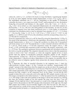
G000, G037, and G087, respectively. Fig.5 shows the magnetic J
c
(B) curves at 5 K and 20K for
all the samples, which were sintered at 850
o
C for 10 hours. The J
c
(B) values for all the doped
samples are higher than the un-doped sample at high fields. The sample G037 gives the
highest J
c
at high fields: J
c
increases by a factor of 30 at 5 K for the field of 10 T, as compared
to the un-doped sample, G000. Even though the J
c
in the low field regime is depressed, a
higher doping level (G087), still results in the rate of J
c
dropping much slower than the un-
doped sample, clearly indicating strong flux pinning induced by the graphene doping. The
most significant effect of graphene doping is the high effectiveness of graphene to improve
flux pinning at lower doping levels, which distinguishes graphene from any other C
containing dopants, for example, the J
c
for G037 reached 20,000 A/cm
2
at 5 K and 8 T,
exceeding or matching the best J
c
resulting from dopants such as SiC, CNT, and
carbohydrates at their optimal doping level of 10 at%, as well as nano-C at its optimal
Applications of High-Tc Superconductivity
208
Fig. 5. Magnetic critical current density as a function of magnetic field at 5 K and 20K for
with and without graphene doped bulk samples. 5 at% nano-C doped sample for a
comparable result at the same sample preparation route (Xu, X. et al., 2010).
doping level of 5-6.4 at.%. In the latter case, the T
c
is substantially reduced to temperatures
as low as 30 K. Compared to the graphite doped MgB
2
pallets prepared through the ball-
milling and HIP the J
c
of graphite doped MgB
2
is better than graphene doping at 5 K
(Yamamoto et al., 2005), but at 20K, the J
c
for graphene doping is much better than graphite.
For example, the J
c
for the graphene doped MgB
2
at 20 K and 6 T is larger than that for
graphite doped MgB
2
by a factor of 50 (Yamamoto et al., 2005). In comparison, low levels of
graphene doping have little effect on T
c
and cause only a very small increase in impurities,
not compromising the significant enhancement in J
c
in high fields by the degradation in low-
field J
c
, which is a common issue for all other C based dopants. In order to see the difference
with other C based dopants, the same preparation route was applied to 5 at% nano-C doped
sample and the resultant decrease in J
c
at 20K can be seen in the figure 5, because the T
c
for
nano- C doped MgB
2
is only 34K.
The transport current J
ct
-B performance of the two kinds of the samples sintered at
temperatures from 700
o
C to 800
o
C, denoted by, WG37S7, WG37S8 for 3.7 at% graphene
doped and WG0S7, and WG0S8 for undoped wire sample, respectively, is shown in Figure
6. It can be clearly seen that J
ct
of samples prepared from the doped wire sample showed
better performance in the field range of 4 to 15 T. This indicates that the most significant
effect of graphene doping is the high effectiveness of graphene to improve flux pinning at
lower doping levels. The strong enhancement in the flux pinning may be attributable to a
combination of C substitution for B and thermal strain-induced defects. It is very surprised
that if compared to the magnetic J
cm
with the bulk MgB
2
samples via a diffusion process
under magnetic fields of 5 to 10 T, the transport J
ct
increment with the wire MgB
2
via the
powder-in-tube (PIT) method is tremendous lower from Fig.6. The transport current
capacity is the real useful J
c
that flows through the whole of the sample. It can be
understand, the difference between J
cm
and J
ct
in MgB
2
may be related to features of the
microstructure of the superconducting MgB
2
core, such as porosity, agglomeration of