Crystalline Silicon Properties and Uses Part 3 pot
Bạn đang xem bản rút gọn của tài liệu. Xem và tải ngay bản đầy đủ của tài liệu tại đây (757.38 KB, 25 trang )
Study of SiO
2
/Si Interface by Surface Techniques
39
Arbitary units
Binding Energy, eV
158 152
0
0.5
1
1.5
2
2.5
3
3.5
4
4.5
5
Arbitary units
Binding Energy, eV
108 100
0
0.5
1
1.5
2
2.5
3
3.5
4
4.5
5
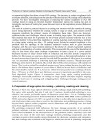
Fig. 15. XPS signal for Si-2p (right) and Si-2s (left) for SiO
2
/Si (blue), SiO
2
(quartz- green),
SiO
2
ion etching 1(red), SiO
2
ion etching 2 (turquoise), SiO
2
ion etching 3 (olive)
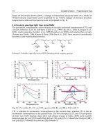
For a better observation of the amorphous surface layer, the cross-section specimen has been
oriented in the microscope along the [110] zone axis as shown in the Selected Area Electron
Diffraction pattern inserted in Fig. 16 (a). This way, the strongly diffracting crystalline
object, the Si wafer, shows a strong dark contrast, allowing to clearly seeing the interface
between the crystalline Si and the amorphous layer on the surface. In the thicker areas of the
TEM specimen, the assembling resin has not been removed during the ion milling
preparation stage (Fig. 16(a)). Here, the limit between the amorphous SiO
2
layer and the
amorphous assembling resin is rather difficult to notice. However, the contrast difference
between the two amorphous materials allows one to measure the thickness of the SiO
2
layer.
One can notice the roughness of the crystalline Si wafer and the amorphous band with a
rather constant thickness (about 2.5±0.5 nm) running along the surface.
In the thinner areas of the specimen (Fig. 16 ( b)), the assembling resin has been removed by
ion milling while a band of amorphous material with the same thickness (2.5±0.5 nm)
running parallel to the crystalline surface is still observable.
We conclude, therefore, that the thickness of the amorphous Si layer on top of the Si(001)
wafer measured by TEM is 2.5±0.5 nm.
Crystalline Silicon – Properties and Uses
40
(a)
(b)
Fig. 16. (a) Cross-section TEM image of the Si surface in a thicker area of the specimen where
the assembling resin is still visible after the ion milling. Inset shows the (b) Cross-section
TEM image of the Si surface in a thinner of the specimen, where the assembling resin has
been removed by ion milling.
As it was stated in previous works [29, 30, 31] the interface between crystalline Si and its
amorphous native oxide SiO
2
is the basis for most current computer technology, although its
structure is poorly understood. In this line, the study of the structural properties of water
near a silica interface by classical and ab-initio molecular dynamics simulations is a part of
this effort. The orientation of water molecules at the interface determined in classical force
fields and quantum simulations [30] show that near the interface the water molecules are
oriented such that at least one of the hydrogen atoms are nearer the silica than the oxygen of
the water molecule. The importance of characterizing the atomic structure of the
Study of SiO
2
/Si Interface by Surface Techniques
41
silicon/silicon dioxide interface as an essential component in highly integrated circuits has
steadily increased as a result of continuing miniaturization of silicon chips.
5. Conclusions
The surface investigations techniques put into evidence the characteristics of Silicon/Oxide
interface as it follows:
- the most important result is the XPS analysis of Si (2p) and Si (2s) signals that are
similar in the interface region
- the XPS signals of Silicon oxides are related to the oxidation states:Si
1+
, Si
2+
, Si
3+
and Si
4+
- the concentration of Si
4+
is higher in the surface region of natural oxidation
- the result of Ion etching of natural SiO
2
(quartz) present the oxidation state Si
3+
- TEM result put into evidence a region of oxide at the surface that has the properties of
the interface including its irregularities, at a thickness of the amorphous Si layer of the
Si (001) wafer measured by TEM is 2.5±0.5 nm.
6. References
[1] F. J. Himpsel, F.R.Mc Feely, A.Taleb-Ibrahimi and J.A.Yarmoff, Physical Review B, Vol.38,
No.9, pp.6084-6095 (1988)
[2] M. Razeghi Technology of Quantum Devices pp.42 LLC (2010), Springer, ISBN 978-1-4419-
1055-4
[3] F. Yano, A.Hiroaka, T.Itoga, H.Kojima and K.Kanehori ,J.Vac. Sci.Technol A, Vol.13, No.6
pp.2671 (1995)
[4] G. W. Rubloff, J.Vac.Sci.Technol. A, Vol.8, No.3, pp.1857 (1990)
[5] T. Hattori and T.Suzuki, Appl.Phys.Lett, Vol.43, No.5 pp.470 (1983)
[6] R. Haight and L.C.Feldman, J.Appl.Phys, Vol.53, pp.4884 (1982)
[7] F.J.Grunthaner, P.J. Grunthaner, R.P.Vasquez , B.F.Lewis and J.Maserjian,
J.Vac.Sci.Technol 16 pp.1443 (1979)
[8] A. Kalnitshi, S.P.Tay, J.P.Ellul, S.Chongsawangvirod, J.W.Andrews and E.A Irene
J.Electrochem. Soc. 137, pp.235 (1990)
[9] Z. H. Lu, J.P.Mc Caffrey, B.Brar, G.D.Wilk, R.M. Wallace, L.C.Feldman and S.P. Tay,
Appl.Phys Lett. Vol.71 No.19, pp.2764 (1997)
[10] R. Held, T.Vancura, T.Heinzel, K.Ensslin, M.Holland, W.Wegscheider,
Appl.Phys.Lett,Vol.73, No.2 pp.262 (1998)
[11] The physics of SiO
2
and its Interfaces
edited by Sokrates T.Pantelides (Pergamon, New
York, 1978)
[12] F. J. Grunthaner and P.J.Grunthaner, Mater, Sci Rep. 1, pp.65 (1986)
[13] Proceedings of the 173-rd meeting of the Electrochemical Society, Atlanta, Georgia, 1988,
edited by C.R.Helms
[14] F. Rochet, S.Rigo, M.frament, C.D’Anterroches, C.Maillot, H.Roulet and G.Dufour,
Adv.Phys. 35, pp.237 (1986)
[15] F. Herman, R.V.Kasowski J.Vac.Sci.Technol, 19,pp.395 (1981)
[16] A. Ourmazd, D.W.Taylor, J.A.Rentschles and J.Bevk, Phys.Rev.Lett, 59, pp.213 (1987)
[17] L. Ohdomari, H.Akatsu, Y.Yamakoshi and K.Kishimoto J.Appl.Phys 62, 3751 (1987)
[18] R. V. Ghita, C.Negrila, A.S.Manea, C.Logofatu, M.Cernea, M.F.Lazarescu,
J.Optoelectron.Adv.Mater, 5, pp.859 (2003)
Crystalline Silicon – Properties and Uses
42
[19] S. Tanuma, C.J.Powell and D.R.Penn, Surf.Interface Anal 21,pp.165 (1994)
[20] S. Tanuma, C.J.Powell and D.R.Penn,Journal of Electron Spectroscopy and Related
Phenomena 52, pp.285 (1990)
[21] S. Tanuma, C.J.Powell and D.R.Penn, Surface Science 192, L 849 (1987)
[22] H. Bethe, Ann.der Physik, 5 pp.325 (1930)
[23]
[24] C. C. Negrila, C.Cotirlan, F.Ungureanu, C.Logofatu, R.V.Ghita, M.F.Lazarescu,
J.Optoelectron. Adv.Mater, 10 (6), pp.1379 (2008)
[25] Freiberger General Specifications, issue 200
[26] (www.fem-semcond.com/pdf/gen.spec.pdf)
[27] T. Hou, C.M.Greenlief, S.W.Keller, L.Nelen and J.F.Kauffman, Chem. Mater. 9,pp.3181
(1997)
[28] C. C. Negrila, C.Logofatu, R.V.Ghita, C.Cotirlan, F.Ungureanu, A.S.Manea,
M.F.Lazarescu, J.Crystal Growth, Vol.310, No.7t-9, pp.1576 (2008).
[29] J. L. Sullivan, W.Yu and S.O.Saied, Surface and Interface Analysis, Vol.22, pp.515 (1994)
[30] Y. Tu and J. Tersoff, Thin Solid Films, Vol.400, No.1-2, pp.95(2001)
[31] Ch. D. Lorenz, M.Tsige, Susan B.Rempe, M.Chandross, M.J.Stevens, G.S.Grest Journal
of Computational and Theoretica Nanoscience, Vol.7, No.12, pp.2586 (2010)
[32] S. Bergfeld, B.Braunschweig, W.Daum, Physical Review Letters, Vol.93, No.9 (2004)
3
Effect of Native Oxide on the
Electric Field-induced Characteristics
of Device-Quality Silicon at Room Temperature
Khlyap Halyna, Laptev Viktor, Pankiv Lyudmila and Tsmots Volodymyr
1
State Pedagogical University, Drohobych
2
Russian New University, Moscow
1
Ukraine
2
Russian Federation
1. Introduction
There is no needing emphasize about the importance of silicon (Si) as a material of choice for
almost all fields of the new nano- and microelectronics. Due to its unique structural and
physical properties, polycrystalline Si seems to be of special interest as a base for creating
so-called 3D-integrated circuits.
Various studies have established the main processes of carrier transport in the structures
based on this material. In particular, it was shown that tunneling and diffusion
recombination processes dominate under room temperature and applied low electric fields.
Nevertheless, the analysis and numerical simulation of the experimental data do not always
take into account the finite dimensions of the investigated structure and the appearance of
carrier depletion as an important component of the tunneling current observed
experimentally. Besides that, the fabrication of any device based on polycrystalline Si
requires high-temperature treatment. Therefore, the effect of such a treatment on the electric
properties of polycrystalline, amorphous and monocrystalline Si is also seemed to be
important. Regardless of the huge number of publications describing numerous
characteristics of the material and structures based on polycrystalline Si of various types of
conductivity, the question about room temperature carrier depletion (exclusion from the
contact regions) in polycrystalline material is still open.
As is known, native oxides of about 5-10 nm thickness are formed on surfaces after finishing
growth of semiconductor bulk materials or deposition (by molecular beam epitaxy,
modified liquid phase epitaxy, laser ablation, high-temperature treatment, etc.) of thin films
immediately after excluding the samples from the technological chamber. These ultrathin
layers form additional potential barriers which can sufficiently affect the performance of
active elements.
This chapter reports experimental data resulted from the investigations of room-temperature
current-voltage (IVC) and capacitance-voltage (CVC) characteristics performed on amorphous
silicon thin films fabricated by the magnetron sputtering technique and bulk crystalline silicon
of device quality grown by Czochralsky method. The low-resistive contact pads were placed
on front and faceplate surfaces of the samples. Studies of room-temperature electric field-
Crystalline Silicon – Properties and Uses
44
induced characteristics for these structures are seemed to be important for analyzing operation
of multi-element devices (for example, integrated circuits). It was found out that experimental
IVC’s and CBC’s are similar to those of metal-insulator-semiconductor structures. These
results are analyzed in framework of semiclassical theory of semiconductor devices.
2. Photosensitivity of amorphous silicon thin films prepared by magnetron
sputtering
Amorphous silicon is a unique material for design of a large number of novel optoelectronic
and photovoltaic devices. Structures Me/-Si and -Si thin films are the elements of choice
not only for fundamental studies but also for practical applications and numerical
simulations of their properties.
Examination of photosensitive and external electric field-induced characteristics of these
structures is of particular interest. Metal-semiconductor junctions Al/-Si were chosen as an
object of the room temperature investigations. Amorphous silicon thin films (thickness up to
300 nm) were manufactured by magnetron sputtering technology in the range of the current
density (10
-9
-10
-7
) A/cm
2
at T = 300 K.
Current-voltage characteristics nd photosensitivity of the samples was carried out under
normal atmospheric conditions before and after the treatment of the structures in molecular
hydrogen. The hydrogenation of the samples was provided by the special chamber filled
in with molecular H2 during 24 hours at T = 400
0
C and the gas pressure P
H
= 2500 Pa
(Khlyap, 2003).
Fig. 1. Sketch of the experimental sample.
The experimental setup is plotted in Fig. 1. -Si layers of 1 μm thickness were deposited on
the glass substrate by magnetron sputtering under activation of SiH
4
(silane) plasma
dissociation at alternate pulse bias with 55 Hz frequency. Pressure and temperature in the
growth chamber were P = 70 Pa and 225
0
C, respectively. Aluminum (Al) contacts doped
with silicon (1% Si) were manufactured through the mask of 1 mm diameter. The
investigated structure had been connected to the experimental measurement equipment.
Current-voltage characteristics were measured at room temperature under illumination by
UV-, near-IR and visual spectral ranges.
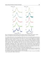
The experimental current-voltage characteristics (IVC) of the investigated samples are
illustrated by Fig. 2. The experiment was carried out under various illuminations. The IVCs
obtained under the background illumination (daylight, curve 1) and under irradiation by
the light source with 100 W power (curve 2) are approximated by the following expression:
Effect of Native Oxide on the Electric Field-induced
Characteristics of Device-Quality Silicon at Room Temperature
45
I
exper
~(V
a
)
m
, (1)
where m < 1.
IVCs of the structures obtained after irradiation by the light source with wavelengths in the
near-IR spectral region (curve 3) and by the UV source (curve 4) can be expressed as
I
exper
~I
s
exp(eV
a
/k
B
T)
m
, (2)
where I
s
is a saturation current defined by the parameters of the film (charge carrier mobility
and the dangling bonds density as well as by the tunneling transparency coefficient of the
Al - -Si barrier (Terukov, 2000&2001).
Fig. 2. Current-voltage characteristic of the investigated sample (T = 300 K) (Khlyap, 2003).
Fig. 3. Current-voltage characteristics of the investigated structure in double-log scale
(Khlyap, 2003).
Re-building the experimental IVC in double-log scale (Fig. 3) allows obtaining more detail
information about current mechanisms in the structures investigated.
0 20406080100
1E-10
1E-9
1E-8
4
2
3
1
Current I, A
Applied voltage V
a
, V
1 - daylight
2 - 100 W light
3 - 760 nm light source
4 - 400 nm light source
110100
1E-10
1E-9
1E-8
4
2
3
1
Current I, A
Applied voltage V
a
, V
1 - daylight
2 - 100 W light
3 - 760 nm light source
4 - 400 nm light source
Crystalline Silicon – Properties and Uses
46
It is obvious that all the experimental current-voltage dependencies are approximated by
straight lines. According to the model (Terukov, 2001; Sze, 2007) one can suggest the
following explanation: the investigated samples are high-resistive films with one group of
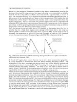
the trap centers localized up the bottom of the conduction band (Fig. 4, Terukov, 2002).
Appearance of these centers causes the space charge limited current (SCLC).
Fig. 4. Schematic drawing of the energy levels in the forbidden gap of amorphous silicon
under thermodynamic equilibrium. E
t
is the trap level, F
0
is the Fermi level position
(Terukov, 2000&2001).
In absence of the external electric field the initial electron concentration in the investigated
films is low and determined by the localization of the Fermi level of the material. In turn, the
Fermi level localization depends on the concentration and the ionization energy of the trap
centers E
t
. Under small applied bias the electrons injected from the Al contacts are confined
by the traps E
t
. As the applied voltage increases, the centers E
t
receive more and more
electrons; at the same time, the concentration of the injected charge carriers is also
increasing. This process is experimentally observed in the linear sections of the IVCs with
different slopes m. UV-radiation accelerates the interaction between the injected charge
carriers and the ones accumulated by the trap centers [Terukov, 2000; Khlyap, 2003).
The IR-photosensitivity of the films is of particular importance. The challenge is that the as-
grown films are quite not photosensitive. One of the simplest ways to make the layers
photosensitive is hydrogenation treatment of the films under certain temperatures. The as-
grown layers were placed in the special chamber filled with the molecular hydrogen for 24
hours at 400
0
C (the gas pressure in the chamber was 2500 Pa). Fig. 5 shows the experimental
current-voltage dependencies.
The experiment showed a sufficient reduction of the films resistance compared with original
values. The slope m has also been changed down to: m ~ 0.6 – 0.7. The photosensitivity in
the near-IR spectral region (~1600 nm) is also sufficiently improved at the applied bias 0-50
V (Khlyap, 2003).
3. Charge carriers exclusion in electronic polycrystalline silicon
The simple and reliable technique of current-voltage characteristics measurements was
applied for studying processes of carrier transport in the electronic polycrystalline silicon
(Reich; Akopian; Khlyap, 2004). The best samples of polycrystalline Si grown by the
c-band
E
t
F
0
v-band
Effect of Native Oxide on the Electric Field-induced
Characteristics of Device-Quality Silicon at Room Temperature
47
Czochralsky method were chosen for the investigations. Specimens of columnar and
granular crystal structure with dimensions 8mm2mm2mm of n-type conductivity were
polished in the solution HNO
3
:HF:CH
3
COOH = 3:1:1 and rinsed in unionized water in order
to maximally avoid the possible influence of surface effects on the results of electrical
measurements. The studies were carried out at room temperature under applied electric
fields 0 – 104 Vm
-1
, corresponding to applied biases in the range of 0 – 190 V.
Fig. 5. Experimental current-voltage characteristics of the investigated samples after
hydrogenation (Khlyap, 2003).
High-temperature (up to 1200
0
C) heat treatment of the samples was performed under
normal atmospheric conditions during 6 h in the furnace of the special construction
providing a stationary temperature gradient along the sample. The measurements of
current-voltage characteristics (IVC) were performed by means of the traditional bridge
method (Sze). Indium contacts were thermally deposited on the lateral facets of the sample.
The left and right contacts will be referred further as the first and the second ones,
respectively. All experimental dependencies are represented in the coordinates of ln j ~
(V
a
)
1/2
, where j is the current density and V
a
stands for the applied voltage. Fig. 6 shows the
IVC of the sample of the columnar polycrystalline-like structure. As one can see, both curves
(“forward” and “reverse”) have no considerable difference, indicating a good quality of
metallic contacts. This IVC demonstrates the domination of at least two-step tunneling with
the threshold voltage V
TR
~ 9 V (Khlyap, 2004).
On the contrary, the IVC of the sample with the granular structure exhibited no asymmetry
between the forward and reverse currents (Fig. 7) (Khlyap, 2004).
High-temperature treatment (1100
0
C) of both samples does not change the IVCs
qualitatively (Fig. 8). However, the resistance of the samples becomes lower and the
threshold voltage of the sample with the columnar structure reduces down to 4 V. Increase
of the treatment temperature up to 1100
0
C does not lead to significant changes of the IVCs in
neither sample.
As we have noted, the dominant process in carrier transport is the tunneling. Nevertheless,
the attempts of numerical simulations of the experimental data according to the theoretical
models developed specifically for tunneling currents (Sze) failed to describe the observed
results, so that we have been forced to take into consideration the phenomena of carrier
0.1 1 10
1E-10
1E-9
1E-8
2
1
Current I, A
Applied voltage V
a
, V
1 - 700 nm light source
2 - 1500 nm light source
T
exper
= 290 K
24 h H
2
heating, 400
0
C, P = 2500 Pa
Crystalline Silicon – Properties and Uses
48
Fig. 6. Forward (curve 1) and reverse (curve 2) currents of the sample with the columnar
structure before high temperature treatment (Khlyap, 2004).
Fig. 7. Current-voltage characteristics of the sample with granular structure before high-
temperature treatment (Khlyap, 2004).
Fig. 8. Current-voltage characteristics of both samples (curve1 corresponds to the sample
with granular structure and curve 2 corresponds to the sample with columnar structure)
after high-temperature (900
0
C) treatment (Khlyap, 2004).
Effect of Native Oxide on the Electric Field-induced
Characteristics of Device-Quality Silicon at Room Temperature
49
depletion and fluctuation of the carrier concentration on the inter-grain boundaries in the
bulk of the sample (Reich, Akopian).
The depletion of charge carriers was observed experimentally and analyzed in the Ge-based
monocrystalline diodes of finite length (Akopian). The effect strongly depends on the
surface recombination velocity, sample length and temperature. The problem is somewhat
more complicated for the structures based on polycrystalline materials, because it is
necessary to take into account the processes of charge transfer along the sub-grain
boundaries. The most important is to estimate the potential distribution in the bulk of the
sample in order o determine the regions of carrier depletion. The potential distribution
caused by the movement of carriers from the first contact toward the second one is
described by the following expression (Akopian):
U = (k
B
T/e)[lj(D
ni
)-1 – 6l
2
(n
0
)3/L
2
n
i
(2n
0
+ n
i
)], (3)
where l is the length of the sample, j is the charge carriers flow, L = [(2D
n
D
p
/(D
n
+ D
p
)]
1/2
,
D
n,p
are the diffusion coefficients for electrons and holes and = 10
-8
s is the lifetime of the
carriers (this value is accepted to be the same for both electrons and holes), n
0
= 10
10
cm
-3
stands for the intrinsic electron concentration, and n
i
= 10
18
cm
-3
takes care of the carrier
concentration immediately involved in the charge transfer. Numerical estimations were
carried out for both the samples. The depletion as an almost completely sweep out of the
carriers was observed only for the sample of the columnar structure after the heat treatment
at 900
0
C. The results obtained for this sample are plotted in Fig. 9 for the range of applied
biases 0.2-1.8 V, which seems to be of particular interest for device operation. The linear
character of the calculated potential distribution shows (Khlyap, 2004) a considerable
accumulation of carriers near he second contact region increasing with the increase of the
applied bias
.
Fig. 9. Potential distribution for the sample with columnar structure after high-temperature
(900
0
C) treatment at the applied voltage V
a
, V: (1) 0.2, (2) 0.6, (3) 1.0, (4) 1.4, (5) 1.8 (Khlyap,
2004).
According to the theory developed in (Reich et al.), the tunneling current j reads as follows:
ln(j/j
0
) = (-1/5)(2/)
1/2
(U
0
/E
B
)
5/4
[n
i
(a
B
)
3
]
-1/2
, (4)
Crystalline Silicon – Properties and Uses
50
where U
0
is the height of the barrier, E
B
= me
4
/(h
2
/2
2
)
2
and a
B
= (h
2
/4
2
)
2
/me
2
are the Bohr
radius and energy for the electron, m
e
is the effective mass, is the dielectric constant of Si,
and j
0
stands for the saturation current. The calculation based on experimental data has
demonstrated that the barrier height U
0
before the heat treatment of the samples is 0.48 eV
and 0.36 eV for the granular and columnar samples, respectively. After heat treatment under
900
0
C these values are 0.12 and 0.9 eV, respectively (Khlyap, 2004).
In summary, current-voltage characteristics and the effect of the high-temperature heat
treatment (900 – 1100
0
C) on carrier transfer in bulk polycrystalline Si of granular and
columnar structures have been investigated. The temperature 900
0
C has been shown to be
optimal for i) reduction of the barrier height in samples of granular structure and ii) a
considerable accumulation of carriers in the region of the second contact. The first
experimental results reported in (Khlyap, 2004) demonstrated the possibility of additional
accumulation of charge carriers in bulk polycrystalline Si of n-type conductivity after high
temperature treatment without sufficient increase of the applied electric field (Khlyap, 2004).
4. Electric characteristics of the structure bulk silicon – native oxide
As we have mentioned above, the native oxide formed immediately after the sample
preparation (a bulk specimen or a thin film) is an unavoidable factor of any technological
process and the following design of the active element. We have investigated room-
temperature electrical (current-voltage, IVC, and capacitance-voltage, CVC) characteristics
of the structure bulk silicon-native oxide. The scheme of the contacts (idium pads) deposited
on the bulk silicon sample is illustrated in Fig. 10.
Fig. 10. Schematic image of In-contact pads deposited on the bulk crystalline silicon sample
for the room-temperature electric investigations.
We have focused on examining the current-voltage functions registered under the
application of external electric field in directions ‘1-2” and “2-1” as well as in directions “1-3,
2-3” and “3-1, 3-2”. The sets of the device-quality crystalline silicon of n-type conductivity
were chosen for this experiment. The samples were cut off from the as-grown ingots.
The experimental electric field-induced characteristics are plotted in Fig.11, a-c. Obvious
that all the experimental current-voltage functions are described by the power law I~(F
a
)
m
,
where F
a
is an applied electric field, and m is an exponential factor determining the mode of
the charge carriers transfer through the sample as a finite volume (directions 1-2 and 2-1)
and through the sample volume – sample surface space (direction 1-3). The numerical
analysis performed in the frame of the semiclassical model (Sze) demonstrated that the
carriers flow through the volume of the sample according to the ballistic – diffusion mode
(the forward current, Fig.11, a), and the dominant tunneling current is observed for the
Effect of Native Oxide on the Electric Field-induced
Characteristics of Device-Quality Silicon at Room Temperature
51
reverse current (Fig.11, b). The tunneling current is also observed for the direction 1-3
(Fig.11, c), but as the applied electric field increases, the tunneling process begins to be
suppressed by the diffusion of the curries due to lowering the potential barrier formed by
the native oxide.
a)
b)
c)
Fig. 11. Room-temperature electric field-induced characteristics of the structure bulk
crystalline silicon-native oxide; a) contacts 1-2, b) contacts 2-1, c) contacts 1-3 (see notes in
Fig.10).
Crystalline Silicon – Properties and Uses
52
Thus, these experimental data are of the barrier type which is more typical for as-prepared
metal-semiconductor structures. To confirm this conclusion we have made the capacitance-
voltage measurements at T = 290 k and the test signal frequency f = 1 kHz. The experimental
results are plotted in Fig.12, a-c.
a)
b)
c)
Fig. 12. Room-temperature capacitance-voltage characteristics of the investigated structure
under the test signal frequency f = 1 kHz: a) contacts 1-2; b) contacts 1-3 (see notes in Fig.10);
c) a control metal-semiconductor structure (In-mono-n-Si).
Effect of Native Oxide on the Electric Field-induced
Characteristics of Device-Quality Silicon at Room Temperature
53
The experimental data have allowed calculating some main parameters of the structure bulk
crystalline silicon-native oxide according to the theory (Sze). The results are listed in Table 1.
Charge
centers
concentration
Contact
Space
charge region
width
Diffusion
potential
N
01
=1.2610
12
cm
-2
N
02
=7.0510
12
cm
-2
1-2
W
01
=14.8 m
W
02
=14.9 m
V
d1
= 0.53 V
V
d2
=1.40 V
N
01
=1.6210
13
cm
-2
N
02
=1.9410
13
cm
-2
2-3
W
01
=15.5 m
W
02
=15.5 m
V
d1
= 3.50 V,
V
d2
= 4.20 V
Table 1. Electric parameters of the investigated structure.
5. Electric parameters of the structure recrystallized nanocrystalline silicon-
Cu/Ag-nanocluster contacts
The unique room-temperature electrical characteristics of the porous metallic nanocluster-
based structures deposited by the wet chemical technology on conventional silicon-based
solar cells were described in (Laptev & Khlyap, 2008). We have analyzed the current-
voltage characteristics of Cu-Ag-metallic nanocluster contact stripes and we have
registered for the first time dark currents in metallic structures. Morphological
investigations (Laptev & Khlyap, Kozar et al., 2010) demonstrated that copper particles
are smaller than 0.1 μm and smaller than the pore diameter in silver. The contacts were
deposited on nanocrystalline silicon structures obtained by the pulse laser
recrystallization of the silicon thin films grown on insulator substrates. The experimental
results are illustrated in Fig.13.
The numerical analysis showed the following results: the first section of forward current
I = T
tun
A
el
(4/9L
2
)(2e/m*)
1/2
(V
a
)
3/2
(ballistic mode) and the second one as
I = T
tun
A
el
(2v
s
/L
2
)V
a
,
and the reverse current is
I = T
tun
A
el
(2v
s
/L
2
)V
a
(velocity saturation mode). Here T
tun
is a tunneling transparency coefficient of the
potential barrier formed by the ultrathin native oxide films, A
el
and L are the electrical
area and the length of the investigated structure, respectively, is the electrical
permittivity of the structure, m* is the effective mass of the charge carriers in the metallic
Cu-Ag-nanoclucter structure, and v
s
is the carrier velocity (Kozar et al., 2010). These
experimental data lead to the conclusion that the charge carriers can be ejected from the
pores of the Cu-Ag-nanocluster wire in the potential barrier and drift under applied
electric field (Sze & Ng, 2007; Peleshchak & Yatsyshyn, 1996; Datta, 2006; Ferry &
Goodnick, 2005; Rhoderick, 1978).
Crystalline Silicon – Properties and Uses
54
Fig. 13. Room-temperature current-voltage characteristics of the structure recrystallized
nanocrystalline silicon-Ag/Cu-nanocluster contacts.
6. Conclusions
The chapter presented here reviews the principal experimental results obtained under
simple and reliable room-temperature electric measurements of the structures based
on various type of device-quality silicon with taking into account the effect of ultrathin
native oxide films unavoidably formed after the preparation of the active element.
Amorphous silicon thin films prepared by the magnetron sputtering technology have
showed good photosensitive properties. Polycrystalline bulk silicon samples were
investigated after the high-temperature treatment in order to clarify this effect on electrical
performance of the active elements (in particular, future ICs). The necessity of different
placement of contact pads on bulk crystalline silicon samples have forced us to
concentrate on the examination of the IVC and CVc of the structures formed by the silicon
samples and the native oxide. These investigations demonstrated that the influence of the
native oxide ultrathin films forming additional (sharp or graded) potential barriers is to
be taken into account under many technological processes using for the device design.
And, the attempting to solve the problem of the performance of low-cost high-effective
solar cells based on conventional silicon resulted in unique chemical wet deposition
technology which has allowed producing Ag/Cu-nanoclustered structures on
recrystallized nanocrystalline silicon. Their current-voltage characteristics are similar to
those of semiclassical metal-semiconductor structures
Effect of Native Oxide on the Electric Field-induced
Characteristics of Device-Quality Silicon at Room Temperature
55
7. References
Akopian A.A. et al. (1987), Charge Carrier Exclusion in Ge-Diodes, Semiconductors (Russia),
Vol. 21, p. 1783.
Datta S. (2006). Quantum transport: Atom to Transistor, Cambridge Univ. Press, ISBN 0-521-
63145-9, Cambridge, Great Britain.
Ferry D. & Goodnick S. (2005). Transport in Nanostructures, Cambridge Univ. Press, ISBN 0-
521-66365-2, Cambridge, Great Britain
Khlyap H. et al. (2003), Photosensitive Amorphous Si Thin Films Prepared by Magnetron
Technology, Proceedings of the Materials Research Society, Fall 2002, Boston, USA, Vol.
744, paper No. M5.20.1.
Khlyap H. et al. (2004), Depletion of charge carriers in electronic polycrystalline silicon,
Mater Science in Semicond Processing, Vol. 7, p. 443-446.
Kozar T. V., Karapuzova N. A. & Laptev G. V., Laptev V. I., Khlyap G. M., Demicheva O. V.,
Tomishko A. G., Alekseev A. M. (2010). Silicon Solar Cells: Electrical Properties of
Copper Nanoclusters Positioned in Micropores of Silver Stripe-Geometry Elements,
Nanotechnologies in Russia, Vol. 5, № 7-8,
p.549-553, DOI: 10.1134/S1995078010070165, ISSN: 1995-0780 (print), ISSN: 1995-
0799 (online).
Laptev V.I. & Khlyap H. (2008). High-Effective Solar Energy Conversion: Thermodynamics,
Crystallography and Clusters, In: Solar Cell Research Progress, Carson J.A. (Ed.), pp.
181–204, Nova Sci. Publ., ISBN 978-1-60456-030-5, New York, USA.
Martin I. et al. (2004), Improvement of Crystalline Silicon Surface Pasivation by Hydrogen
Plasma Treatment, Appl. Phys. Lett., Vol. 85, p. 1474-1476.
Peleshchak R.M. & Yatsyshyn V.P. (1996). About effect of inhomogeneous deformation on
electron work function of metals, Physics of Metals and Metallography, MAIK Nauka
Publishers – Springer, vol. 82, No. 3, pp.18-26, ISSN Print: 0031-918X, ISSN Online:
1555-6190.
Reich M. et al. (1988), Effect of Barrier Localizd States on Fluctuations of tunneling
Current Through Metal-semicondutor Contact, Semiconductors (Russia), Vol. 22, p.
1979.
Rhoderick E. H., (1978). Metal-semiconductor contacts. Clarendon Press, ISBN 0198593236,
Oxford, Great Britain.
Ristova M. et al. (2003), Study of Hydrogeneted Amorphous Silicon Thin Films
As a Potential Sensor for He-Ne Laser Light Detection, Appl Surf Sci., Vol. 218, p.
44.
Sze S.M. & Ng, K.K. (2007). Physics of semiconductor devices, J. Wiley & Sons, Inc., ISBN 0-471-
14323-5, Hoboken, New Jersey, USA.
Terukov E.I. et al. (2000), Current-Voltage Characteristics of Electroluminescent Me/a-Si:
H<Er>/c-Si Structures Prepared by Magnetron Sputtering, Semiconductors (Russia),
Vol. 34, p. 617-620.
Terukov E.I. et al. (2001), Interrelationship between the Recombination on Interfaces and
Ubnormally Weak Dependence of photoconductivity on Illumination Intensity,
Semiconductors (Russia), Vol.35, No.6, p.643-647.
Crystalline Silicon – Properties and Uses
56
Vasilev I. (2003), Optical Excitations in Small Hydrogenated Silicon Clusters: Comparison of
Theory and Experiment, Phys Stat Sol B , Vol.239, p.19.
4
Structure and Properties of
Dislocations in Silicon
Manfred Reiche
1
and Martin Kittler
2
1
Max Planck Institute of Microstructure Physics, Halle
2
IHP microelectronics, Frankfurt (Oder)
Germany
1. Introduction
Defects in crystalline materials modify locally the periodic order in a crystal structure. They
characterize the real structure and modify numerous physical and mechanical properties of
a crystal. Crystal defects are generally divided by their dimension: point defects are also
known as zero-dimensional (0-D) defects, while dislocations are 1-D, twins and grain
boundaries are 2-D, and precipitates are denoted as 3-D defects. Dislocations were
implemented for the first time in the early 1900th to explain the elastic behavior of
homogeneous, isotropic media. Based on Volterra´s “distorsioni” (Volterra, 1907), Love has
introduced the term “dislocation” to describe a discontinuity of displacement in an elastic
body (Love, 1927). The application of this term to denote a particular elementary type of
deviation from the ideal crystal lattice structure was due to Orowan (1934), Polanyi (1934),
and Taylor (1934a, 1934b).
A dislocation is characterized by a vector parallel to the dislocation line and a displacement
or Burgers vector which is a certain finite increment induced by the elastic displacement
vector . The Burgers vector is equal to one of the lattice vectors in magnitude and direction
and may be written as (Hirth & Lothe, 1982)
∮
=
=−
. (1)
The direction along the contour s is that of a right-hand screw relative to the chosen
direction along the dislocation line ℓ, that is, relative to the unit vector tangent to the
dislocation line (Frank, 1951). The edge dislocation, introduced by Orowan (1934), Polanyi
(1934), and Taylor (1934a, 1934b), is represented by the line ℓ along which the vectors and
are perpendicular. If the vectors and are parallel, then the corresponding dislocation is
called a screw dislocation (Burgers, 1939, 1940). In many materials, dislocations are found
where the line direction and are neither perpendicular nor parallel and these dislocations
are called mixed dislocations, consisting of both edge and screw character.
In the elastic theory of isotropic media a dislocation is a line representing the boundary of
the slipped region. Its strength is characterized by the displacement. The strain field around
the dislocation is depicted as a cylinder. Among other things, the model explains the strain
distribution around the dislocation, but cannot describe the strain in the center, i.e. in the
core of the dislocation. Furthermore, the model does also not regard the influence of the
Crystalline Silicon – Properties and Uses
58
lattice periodicity of real crystals. Burgers & Burgers (1935) as well as Taylor (1934a, b),
Polanyi (1934), and Kochendörfer (1938) already pointed out that a dislocation moves by
skipping individual atoms via potential walls. A first phenomenological model considering
a potential energy of displacement that reflects the lattice periodicity was proposed by
Frenkel and Kontorova (see Dehlinger and Kochendörfer, 1940). The model was modified by
Peierls (1940) and extended by Nabarro (1947). Here, the displacement of the crystal lattice
and the associated stress are considered to be caused by a number of infinitesimal
dislocations originally suggested by Eshelby (1949). For edge dislocations, the width, or core
region, in the Peierls-Nabarro model is given by
2=/(1−) (2)
where d is the lattice plane distance and is the Poisson ratio. The introduction of the
parameter has the effect of removing the singularity at the origin of the dislocation that
is present in model of Volterra (Hirth & Lothe, 1982). For screw dislocations the Peierls-
Nabarro model assumes a stress component near the core which spreads out of the plane.
This phenomenon anticipates the dissociation of a dislocation. The model also explains
the motion of dislocations and results in the introduction of the Peierls energy, which
represents the periodic displacement potential energy, as well as the Peierls stress
required to overcome this potential barrier. The concept of kinks and jogs in dislocation
lines is also a consequence of the model (Friedel, 1979). The Peierls-Nabarro model has
been influential in the development of dislocation theory of more than 60 years. It was, for
instance, modified to explain the dislocation motion (Hirth & Lothe, 1982), or to
understand the structure of the dislocation core (Duesbery & Richardson, 1991; Bulatov &
Cai, 2006).
Early investigations on semiconductor materials indicated the presence of electrically
charged dislocations. It was already proved by Gallagher (1952) that plastic deformation of
silicon and germanium increases their resistivity. Hall effect measurements suggested the
introduction of acceptor-type levels in n-type Ge by deformation which was explained by
negatively charged dislocation lines screened by a positive space charge region (Pearson et
al., 1954). Based on these results and a remark of Shockley that dangling bonds in the core of
an edge dislocation exist, Read (1954a,b) formulated a phenomenological theory of charged
dislocations. He introduced the concept of dislocation electron levels, the occupation ratio of
dislocation levels, and the radius of a Read cylinder surrounding each charged dislocation
and screening the linear charge localized on it. Read (1954a,b) assumed that the dislocation
states are represented by a single level or a one-dimensional band which is empty when the
dislocation is in the neutral state. This assumption is applicable only at low temperatures
(Labusch & Schröter, 1980). On the other hand, Schröter and Labusch (1969) argue that even
at higher temperatures the dislocation band is half filled in the neutral state. Furthermore,
dangling bonds does not exist in real dislocations. Numerous theoretical and experimental
investigation particularly on dislocations in silicon refer to reconstructed dislocation cores.
Therefore the electrical activity is related to defects on the dislocation core, such as kinks,
jogs, and also by point defects bound to the core or in the elastic or electric field of the
dislocation (Schröter & Cerva, 2002). While different types of dislocations are distinguished
by different core defects their electrical activity is different (Alexander & Teichler, 1991). In
addition, the concentration of point defects interacting with dislocations is doubtful even in
the case of elemental semiconductors.
Structure and Properties of Dislocations in Silicon
59
The present chapter reviews the current understanding about the structure and properties of
dislocations in silicon and is based on earlier reviews given for instance by Bulatov et al.
(1995), Alexander & Teichler (2000), Schröter & Cerva (2002), Spence (2007), and Kveder &
Kittler (2008). All these papers demonstrate a substantial progress over the years but show
also that a number of problems such as dislocation mobility, structure of the dislocation
core, or electronic properties are not completely solved (George & Yip, 2001; Spence 2007).
For instance, ab-initio computer simulations using different approaches result in a large
number of models of the core structure of different dislocations which are not verified
experimentally. The experimental data of dislocation motion can only be partially simulated
by limiting the number of atoms, etc. (Bulatov & Cai, 2006). Another problem is the
fundamental difference between theoretical calculations and experiment. While only
individual dislocations are regarded in most of the calculations, a large number of
dislocations is involved in experimental measurements such as plastic deformation. These
measurements integrate not only over a number of dislocations but may also include data of
different dislocation types and the interaction with a more or less unknown concentration of
point defects. A further paragraph of this chapter is therefore dedicated to the preparation
and characterization of only a small number of defined dislocations.
2. Structure of dislocations in silicon
Silicon crystallizes in the cubic diamond structure (space group Fd3m). The lattice constant is
= 0.543 nm. The glide plane is {111} and perfect dislocations have Burgers vectors of the type
=/2
〈
110
〉
. Hornstra (1958) has introduced two types of perfect dislocations in the diamond
lattice: a pure screw dislocation and the so-called 60° dislocation, where the Burgers vector is
inclined at an angle of 60° to the dislocation line. The diamond structure corresponds to two
face-centered cubic (fcc) lattices displaced by
(
14,14,14
⁄⁄⁄)
. Hence, atoms in both lattices do
not have identical surroundings. Due to this fact, there are two distinct sets of {111} lattice
planes; the closely spaced glide subset and the widely spaced shuffle subset (Hirth & Lothe,
1982). There is a long controversial discussion about the dominant dislocation type in the
diamond structure. Early publications suggest the presence of dislocations in the shuffle set
because movement through one repeat distance on a shuffle plane breaks one covalent bond
per atomic length of dislocation (e.g. Seitz, 1952). The equivalent step on a glide plane involves
the breaking of three bonds (Amelinckx, 1982). The idea of splitting or dissociation of perfect
dislocations in the diamond structure has been commented for the first time by Shockley
(1953) and was experimentally proved later on by electron microscopy. The introduction of the
weak-beam method by Cockayne et al. (1969) has particularly shown that dislocations in
silicon are in general dissociated and glide in this extended configuration. Both the screw and
60° dislocation belonging to the glide set can dissociate into pairs of partial dislocations
bounding an intrinsic stacking fault ribbon (Ray & Cockayne, 1971; Gomez et al., 1975; Gomez
& Hirsch, 1977). On the other hand, screw and 60° dislocations of the shuffle set can only
dissociate into partials bounding an intrinsic stacking fault if there is a row of either vacancies
or interstitials associated with one of the partials (Amelinckx, 1982). Most of the evidence
indicates that the dislocations found in plastically deformed silicon belong to the glide set
(Hirsch, 1985; Alexander, 1986; Duesbery & Joós, 1996).
For the 60° dislocation a 30° partial and a 90° partial dislocation are formed through
dissociation, while the screw dislocation dissociates into two 30° partials (Gomez et al., 1974;
Heggie and Jones, 1982). These is described by the dissociation reaction (Marklund, 1979)
Crystalline Silicon – Properties and Uses
60
→
+
, (3)
where in the case of a 60° dislocation
=
2
[011]
=
6
[
121
]
=
6
111
(4a)
and for a screw dislocation
=
2
[011]
=
6
[
121
]
=
6
211
(4b)
holds. The 30° as well as the 90° dislocations are of the Shockley type. The dissociation result
as well in the formation of a stacking fault between both partial dislocations. The size of the
stacking fault, i.e. the width of the splitting of the perfect dislocations d
0
, depends in a stress
free crystal on the stacking fault energy
SF
and the repulsion force F of the partial dislocations
=
(5)
The repulsion force is calculated using elastic constants given by the linear theory of
elasticity resulting in (Amelinckx, 1982)
=
8
∙
2−
1−
∙1−
2
2−
∙2Θ
(6)
where G is the shear modulus, and the angle between the dislocation line and the Burgers
vector of the perfect dislocation. In a stressed crystal the two partials are exposed to
additional forces which are in general different. Depending on the crystallographic
orientation the external stress causes an increase or a decrease of d
0
. Therefore the width of
the splitting of a dislocation d
D
by applying a resolved shear stress
s
is given by (Wessel &
Alexander, 1977)
=
1+
−
1−
1+
∙
2
(7)
with being a geometric factor and =
1
/
2
as the ratio of mobilities
j
of both partial
dislocations.
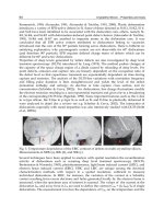
(a) (b)
Fig. 1. Models of the core structure of an unreconstructed (a) and a reconstructed 30° partial
dislocation (b) according to Northrup et al. (1981) and Marklund (1983).
Structure and Properties of Dislocations in Silicon
61
The initial models of perfect dislocations assumed dangling bonds in their core (Shockley,
1953; Hornstra, 1958). Experimental data, however, obtained mainly by electron
paramagnetic resonance (EPR) spectroscopy refer to a low density of such dangling bonds
(Alexander & Teichler, 2000). Dislocations of the glide set reconstruct by dissociation
(Heggie & Jones, 1983; Marklund, 1983; Alexander, 1991), while dislocations of the shuffle
set, which may exist at high applied shear stress, can stabilized by interaction with vacancies
(Li et al. 2008). Different models of the core structure of partial dislocations have been
suggested (figure 1, 2). The model of an unreconstructed 30° partial dislocation was
presented and verified experimentally by high-resolution transmission electron microscopy
(HRTEM) by Northrup et al. (1981). Models of the reconstructed 30° partial dislocation were
proposed by Marklund (1983), Chelikowsky (1982), and Csányi et al. (2000). In this
configuration, the dangling bonds are saturated after the pairs of neighbouring core atoms
move closer together to form bonded dimers. The reconstruction breaks the translation
symmetry and doubles the period along the dislocation line from b to 2b, where b is the
magnitude of the Burgers vector. A defect appears at the boundary between two segments
reconstructed in the opposite sense (so-called antiphase defect (Hirsch, 1979) or soliton
(Heggie & Jones, 1983)).
The core reconstruction of the 90° partial dislocation was studied for more than 30 years.
The driving force for core reconstruction is the same as for the 30° partial, that is the high
energy of the unsaturated dangling bonds. A first model was proposed by Hirsch (1979). In
this reconstruction there is a displacement that breaks the mirror symmetry normal to the
dislocation line, enabling threefold coordinated atoms in the unreconstructed core to come
together and bond. In this way two degenerate reconstructions exist. This core
reconstruction is shown in figure 2a. The symmetry breaking displacement does not alter
the translational symmetry along the dislocation line, which retains the same periodicity as
the crystal (Bulatov et al., 2001). Another core reconstruction was proposed by Duesbery et
al. (1991). In this structure the mirror symmetry is not broken and the atoms on either side of
the dislocation line move towards each other so that each core atom has three nearest
neighbours plus two more neighbours at a somewhat greater distance. This reconstruction is
known as the quasi-fivefold reconstruction. Simulations, however, indicate that the quasi-
fivefold configuration was higher in energy (Bigger et al., 1992). Benetto et al. (1997)
proposed a new core reconstruction for the 90° partial dislocation with double the
periodicity along the dislocation line (figure 2b). They found also that this reconstruction
has a lower potential energy than the single period reconstruction. Further simulations,
(a) (b)
Fig. 2. Models of the core structure of a single period (a) and a double period reconstruction
of a 90° partial dislocation (b) according to Bulatov et al. (2001).
Crystalline Silicon – Properties and Uses
62
however, have shown that the energy differences between the single and double period
structures are very close (Lehto & Öberg, 1998).
3. Electronic properties of dislocations in silicon
Dislocations interfere the translational symmetry of the crystal. As a consequence energy
levels in the band gap result. First analyses were done by Read (1954a, b) who concerned
with long-range screening and occupation statistics in the presence of the macroscopic band
bending due to the dislocation. Based on early experiments of the plastic deformation of
heavily doped p-type Ge single crystals (Gallagher, 1952; Pearson et al., 1954) Read
concluded that only an acceptor level is introduced by edge dislocation. According to this
model the dislocation is negatively charged. The line charge of the dislocation is screened by
ionized donor atoms in a cylinder. Free electrons cannot penetrate this space charge cylinder
and are scattered by specular reflection at its surface. For the position of the energy level of
the neutral dislocation Read (1954a) obtained a value of 0.2 eV below the conduction band.
The acceptor model of the dislocation states was not confirmed by measurements on p-type
Ge and Si with lower doping levels (Schröter, 1969; Weber et al., 1968). It was concluded that
dislocations can act as acceptors and as donors and consequently a partially filled band was
attributed to the dislocation, in agreement with theoretical predictions (Schröter & Labusch,
1969). Veth and Lannoo (1984) combined the models of Read and Schröter & Labusch. They
carried out a self-consistent calculation of the potential in the vicinity of the dislocation,
point to an intraatomic Coulomb term J, and treat screeing in the dislocation core as
dielectric perturbation. Outside the core, classical screeing by ionized dopant atoms or free
carriers take place. The transition between the two screening mechanisms was analyzed.
From this analysis follows a parameter-free formula for the total shift of the dislocation level
E
e
with respect to the edge of the undisturbed valence band
=
+
2
−0.616
(8)
with p as the number of excess electrons per atom, є the dielectric constant, a the distance
between two core atoms, and R as the radius of the screening space-charge cylinder (Read
cylinder), given by
=
(
∙∙
|
−
|)
/
(9)
In Eq. (8) N
D
and N
A
are the concentrations of donors and acceptors, respectively. Veth and
Lannoo (1984) pointed out that Eq. (8) is linear with p, which fits the experimental data with
Read´s model and corresponds to the line charge model by Labusch & Schröter (1980). There
are several problems that have to be solved by any model of the charged dislocation core.
One is the electrostatic potential around a charged dislocation. Another is the mobility of the
charges on the dislocation line.
Computer simulations result in a number of deep levels related to defects on the dislocation
core (Alexander & Teichler, 1991). The energy levels depend strongly on the geometry of the
defects. For instance, the structure and resulting energy levels of 30° partial dislocations
were studied by Marklund (1979), Northrup et al. (1981), Chelikowsky (1982), and Csányi et
al. (2000). Deep levels related to 60° or 90° partial dislocations were summarized by
Alexander & Teichler, 1991). All the computer simulations clearly demonstrate that deep
levels are caused by core bond reconstruction and reconstruction defects. Most of the
Structure and Properties of Dislocations in Silicon
63
models, however, prefer reconstruction defects (antiphase defects, solitons) to explain the
electronic properties of dislocations (Marklund, 1979; Heggie & Jones, 1983; Justo & Assali,
2001). Furthermore, electronic band gap calculations in combination with electron energy
loss spectroscopy of dislocations in GaN revealed that impurities bonded to the dislocation
core may induce electronic levels in the band gap (Bangert et al., 2004). On the other hand,
the interaction of core defects with otherwise electronically active centers can also result in
inactive complexes (Heggie et al., 1993; Jones et al., 1993).
Besides deep levels related to the dislocation core, shallow levels exist corresponding to
more extended states, either states associated with stacking faults between two partial
dislocations or states of electrons and holes trapped in the elastic deformation field of the
dislocation. Calculations of energy levels related to stacking faults refer to the existence of
shallow levels up to 0.1 eV above the valence band edge (Marklund, 1981; Mattheiss & Patel,
1981; Lodge et al., 1989). The shift of point defect levels relative to the silicon band edge may
also be caused by the dislocation strain field. The response of the Si band structure to
homogeneous elastic stresses has been investigated and is described by the deformation
potential Ξ
ij
(Bardeen & Shockley, 1950), which is written for the conduction band edge as
(Keyes, 1960)
Δ
=Ξ
∙
,
(10)
where
ij
denotes the components of the strain tensor. Considering one minimum in the
centre of the Brillouin zone and assuming an elastically isotropic material as an
approximation, the shift of the conduction band minimum is given by the trace of the strain
tensor and one component of the deformation potential tensor, Ξ
d
(Schröter & Cerva, 2002):
Δ
=
∙Ξ
(1−2)
2(1−)
∙
Θ
(11)
In polar coordinate system means the angle between and b
e
, the edge component of the
Burgers vector. If Ξ
d
is positive, the conduction band edge is lowered in the compressed
region of an edge dislocation and increases in its tensile region. The behavior is reverse for
negative values of Ξ
d
. In addition, the strain field results also in an effective shift of the point
defect level. If the strain-induced shift of the point defect level is described by the
deformation potential Ξ
pd
, one obtaines a position-depending shift
E
c
,
pd
of the conduction
band edge and point defect level (Schröter & Cerva, 2002)
Δ
,
=−
(Ξ
−Ξ
)(1−2)
2(1−)
∙
Θ
(12)
Analogous models for 60° and screw dislocations in p- and n-type elemental
semiconductors (Si, Ge) have been proposed by Shikin & Shikina (1995).
The electrical activity of dislocations in silicon and germanium was studied by numerous
methods where mostly plastic deformation was applied to produce defined dislocation
arrangements (for instance, Schröter & Cerva, 2002; Alexander & Teichler, 2000). Hall effect
measurement was primarily applied to verify the electrical activity of dislocations and to
propose first models (Gallagher, 1952; Read, 1954a, b; Schröter & Labusch, 1969). Electron
paramagnetic resonance (EPR) spectroscopy provides substantial information about the
structure and, in combination with other techniques, electronic core defects (Kisielowski-