Crystalline Silicon Properties and Uses Part 13 pdf
Bạn đang xem bản rút gọn của tài liệu. Xem và tải ngay bản đầy đủ của tài liệu tại đây (2.19 MB, 25 trang )
Porous Silicon Integrated Photonic Devices for Biochemical Optical Sensing
289
OP
(ip)
2
N
RO
OP
OR
Si-O
O
Si-OH
ODMT
T
ODMT
T
OP
OR
Si-O
O
+
3
4
2
8
1
i
i
O
T
T
OP
OR
O
O
OH
T
OP
OR
O
R = CH
2
CH
2
CN
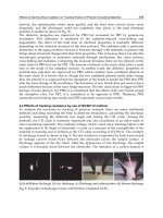
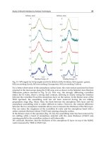
Fig. 16. Scheme of the solid phase synthesis of the 10 bases oligonucleotide
4 on the PSi-OH
surface
1 using 5'-dimethoxytrityl-thymidine-phosphoramidite 2; i: standard automatic
synthetic cycle (Rea et al., 2010).
In order to quantify the surface functionalization, we have removed the 5'-dimethoxytrityl
(DMT) protecting group from the support-bound 5’-terminal nucleotide by using
the deblocking solution of trichloroacetic acid in dichloromethane (3% w/w). The release of
the protecting group generates a bright red-orange colour solution in which the quantity
of the DMT cation could be measured on-line by UV-VIS spectroscopy at 503 nm
(ε = 71700 M
-1
cm
-1
). The Figure 17 shows the DMT analysis performed on the PSi device
after each synthesis cycle: the amount of DMT indicated reaction yields over 98%. These
values resulted almost steady during the ON growing process, confirming the stability of
the chip surface and the high accessibility of ON 5'-OH end groups By averaging over these
values, we have estimated a functionalization degree of 3.25 nmol/cm
2
. The presence of ON
chains bonded on the chip has been also verified by spectroscopic reflectometry. The
biological molecules, attached to the PSi pore walls, induce an increase in the average
refractive indexes of the layers, causing a red-shift in the reflectivity spectrum of the Bragg
mirror. The magnitude of the shift increases with the increase of the pores surface coverage
with the organic matter. The reflectivity spectra of the PSi multilayered structure before and
after the ON synthesis are reported in Figure 18. A red-shift of 11 nm has been measured.
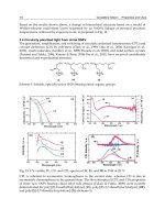
T1 T2 T3 T4 T5 T6 T7 T8 T9 T10
1.2
1.4
1.6
1.8
2.0
2.2
UV Intensity (a. u.)
ON synthesis (3'5')
Fig. 17. DMT measurements performed on the sample after each synthesis cycle.
5. Integrated microfluidic porous silicon array
The microarray technology has demonstrated a great potential in drug discovery, genomics,
proteomics research, and medical diagnostics (Pregibon et al., 2007; Poetz et al., 2005;
Crystalline Silicon – Properties and Uses
290
600 650 700 750 800 850 900
0.0
0.2
0.4
0.6
0.8
1.0
Reflectivity (a. u.)
Wavelength (nm)
after Piranha treatment
after DNA synthesis
=+11 nm
Fig. 18. Reflectivity spectra of the Bragg mirror before (solid line) and after (dash line) the
oligonucleotide synthesis.
Nishizuka et al., 2003). The key issue is the very high throughput of these devices due to the
large number of samples that can be simultaneously analyzed in a single parallel
experiment. Further advantages are fast time analysis and the consumption of very small
amount of reagents. The microarray technology is based on the immobilization of a large
number of highly specific recognition elements on a solid platform. Different types of
platform surfaces have already been explored; the most common examples are derivatized
glass and gold/aluminium substrates (MacBeath & Schreiber, 2000; O’Connor & Pickard,
2003). Silicon, and silicon related materials, is by far the most important and diffuse material
for lab-on-chip applications due to the high development of the integrated circuits
technology. Recently, porous silicon substrates have been proposed for reverse phase
protein and DNA microarray (Ressine et al., 2007; Chen et al., 2009; Yamaguchi et al., 2007):
small sensing area with high detection efficiency is the key feature in both applications, in
which quantitative signals are generated by fluorescence and infrared spectroscopy,
respectively. Alternatively, we have studied the fabrication process and the optical
characterization by reflectometry of a microarray of PSi photonic devices as functional
platform for label-free detection of biomolecular interactions (Rea at al., 2010b). The array
support has been integrated with a microfluidic circuit made of polydimethylsiloxane
(PDMS) which strongly reduces the functionalization time, chemical and biological products
consumption, while it preserves all the features of the PSi label-free optical detection.
5.1 Fabrication and optical characterization of the PSi Bragg mirror microarray
The integration of the PSi elements in a microarray is not straightforward. To this aim a
proper technological process has been designed. The process flow chart of the PSi µ-array
fabrication is schematized in Figure 1. The silicon substrate was a highly doped p
+
-type
wafer with a resistivity of 0.01 Ω cm, <100> oriented and 400 µm tick. Silicon nitride has
been used as masking material during the electrochemical etching since it shows a better
resistance against the HF solution with respect to photoresist, which effectively protects the
silicon only for 2-3 min (Tao & Esashi, 2004). The silicon nitride film, 1.6 μm thick, was
deposited by PECVD on the substrate (Figure 19 (a)). A standard photolithographic process
Porous Silicon Integrated Photonic Devices for Biochemical Optical Sensing
291
was used to pattern the silicon nitride film (Figure 19 (b)), which has been subsequently
etched by RIE process in CHF
3
/O
2
atmosphere (Figure 19 (c)). Finally, the silicon wafer was
electrochemically anodized in a HF-based solution (50 wt. % HF : ethanol = 1:1) in dark and
at room temperature (Figure 19 (d)). We have realized the Bragg reflectors by alternating
high (H) refractive index layers (low porosity) and low (L) refractive index layers (high
porosity); a current density of 80 mA/cm
2
was applied to obtain low refractive index layers
(n
L
=1.6) with a porosity of 71 %, while one of 60 mA/cm
2
was applied for high index layers
(n
H
=1.69) with a porosity of 68 %. The device was then fully oxidized in pure O
2
.
Fig. 19. Technological steps of the PSi µ-array fabrication process.
The optical microscope image of the microarray and the reflectivity spectra of some Bragg
mirror elements are reported in Figure 20. The diameter of each element is of 200 µm, but it
can be reduced to about 1 µm, by changing properly the photolithographic mask. The
reflectivity spectra at normal incidence of the Bragg devices are characterized by a
resonance peak at 627 nm and a FWHM of about 25 nm. The spectra demonstrate also the
uniformity of the electrochemical etching on the whole microarray surface.
Fig. 20. Optical microscope image of the microarray and reflectivity spectra of the PSi Bragg
mirrors.
5.2 Integration of the PSi array with a microfluidic system
The microfluidic system was designed by a computer aided design software. The pattern
was printed 10 times bigger than its real size on a A4 paper by a laser printer (resolution
1200 dpi) and then transferred on a photographic film (Maco Genius Print Film) by a
Crystalline Silicon – Properties and Uses
292
photographic enlarger (Durst C35) reversely used. The designed fluidic system was
replicated by photolithographic process on a 10-μm thick negative photoresist (SU-8 2007,
MicroChem Corp.) spin-coated for 30 s at 1800 rpm on a silicon substrate. After the
photoresist development (SU-8 developer, MicroChem Corp.), the silicon wafer was
silanized on exposure to chlorotrimethylsilane (Sigma-Aldrich Co.) vapour for 10 min as
anti-sticking treatment. A 10:1 mixture of PDMS prepolymer and curing agent (Sylgard 184,
Dow Corning) was prepared and degassed under vacuum for 1 hour. The mixture was
poured on the patterned wafer and cured on a hot plate at 75°C for 3h to facilitate the
polymerization and the cross-linking process. After the PDMS layer peeling, inlet and outlet
holes were drilled through it in order to allow the access of liquid substances to the system.
Finally, the PDMS layer was rinsed in ethanol in a sonic bath for 10 min. The surfaces of
PDMS layer and microarray, whose PSi elements were thermally oxidized, were activated
by exposing to oxygen plasma for 10 sec to create silanol groups (Si-OH) as shown in the
schematic reported in Figure 21, aligned under a microscope using an x-y-z theta stage, and
sealed together. After the sealing with the PDMS system, the PSi elements of the array have
been functionalized with DNA single strand, as described in section 4.1. The microfluidic
circuit allows to use only few microlitres (~5 l) of biologicals with respect to the tens of
microlitres used in the case of not integrated devices. Moreover, the incubation time has
been also reduced from eight to three hours. After the bio-functionalization with DNA
probe, we have studied the DNA-DNA hybridization by injecting into the microchannel 200
µM of complementary sequence. Figure 22 shows the reflectivity spectra of a PSi Bragg
mirror after the DNA functionalization and after the complementary DNA interaction. A
red-shift of 5.0 nm can been detected after the specific DNA-DNA interaction. A negligible
shift, less than 0.2 nm (data not reported in the figure), is the result of a control
measurement which has been done exposing another functionalized microchannel to non-
complementary DNA, demonstrating that the integrated PSi array is able to discriminate
between complementary and non-complementary interactions.
Fig. 21. Scheme of the fabrication process used to integrate the PSi array with a PDMS
microfluidic system.
6. Conclusion
The PSi technology allows the fabrication of different multilayered devices with complex
photonic features such as optical resonances and band gaps. These photonic structures,
functionalized with a biomolecular probe able to selectively recognize a biochemical target,
have been successfully used as label-free optical biosensors. The sensing mechanism is
based on the increase of the PSi refractive index due to the infiltration of the biological
Porous Silicon Integrated Photonic Devices for Biochemical Optical Sensing
293
540 560 580 600 620
0.2
0.4
0.6
0.8
1.0
Reflectivity (a. u.)
Wavelength (nm)
DNA
cDNA
=5 nm
Fig. 22. Reflectivity spectra of a PSi Bragg mirror after the DNA probe attachment (solid
line), and after the hybridization with the complementary DNA (dash line).
substances into the nanometric pores of the material; the consequence of the refractive index
change is the shift of the reflectivity spectrum of the photonic devices. Since PSi technology
is compatible with the microelectronic processes, it can be easily used as functional platform
in the fabrication on integrated microsystems. As example, we have reported the realization
of a PSi microarray for the detection of multiple DNA-DNA interactions. The array,
characterized by a density of 170 elements/cm
2
, has been integrated with a microfluidic
system made of PDMS which allows to reduce the consumption of the chemical and
biological substances.
7. References
Anderson, S.H.C.; Elliot, H.; Wallis, D.J.; Canham, L.T. & Powell, J.J. (2003). Dissolution of
different forms of partially porous silicon wafers under simulated physiological
conditions. Phys. Status Solidi A, Vol. 197, pp. 331-335.
Anderson, M.A.; Tinsley-Brown, A.; Allcock, P.; Perkins, E.A.; Snow, P.; Hollings, M.; Smith,
R.G.; Reeves, C.; Squirrell, D.J.; Nicklin, S. & Cox, T.I. (2003). Sensitivity of the
optical properties of porous silicon layers to the refractive index of liquid in the
pores. Phys. Stat. Sol. A, Vol. 197, pp. 528-533.
Aspnes, D.E. & Theeten, J. B. (1979). Investigation of effective-medium models of
microscopic surface-roughness by spectroscopic ellipsometry. Physical Review B,
Vol. 20, pp. 3292-3302.
Brandenburg, A. & Henninger, R. (1994). Integrated optical Young interferometer. Applied
Optics, Vol. 33, pp. 5941-5947.
Canham, L.T. (1990). Silicon quantum wire array fabrication by electrochemical and
chemical dissolution of wafers. Appl. Phys. Lett., Vol. 57, pp. 1046-1048.
Crystalline Silicon – Properties and Uses
294
Chan, S.; Horner, S.R.; Fauchet, P.M. & Miller, B.L. (2001). Identification of Crom Negative
Bacteria using nanoscale silicon microcavities. J. Am. Chem. Soc., Vol. 123, pp. 11797-
11798.
Chandrasekaran, A.; Acharya, A.; You, J.L.; Soo, K. Y.; Packirisamy, M.; Stiharu, I. &
Darveau, A. (2007). Hybrid integrated silicon microfluidic platform for fluorescence
based biodetection. Sensors, Vol. 7, pp. 1901-1915.
Chen, L.; Chen , Z.T.; Wang , J.; Xiao , S.J.; Lu, Z.H.; Gu, Z.Z.; Kang, L.; Chen, J.; Wu, P.H.;
Tang, Y.C. & Liu, J.N. (2009). Gel-pad microarrays templated by patterned porous
silicon for dual-mode detection of proteins. Lab on a Chip, Vol. 9, pp. 756-760.
Dancil, K.P.S.; Greiner, D.P. & Sailor, M.J. (1999). A porous silicon optical biosensor:
Detection of reversible binding of IgG to a protein A-modified surface. J. Am. Chem.
Soc., Vol. 121, pp. 7925-7930.
De Stefano, L.; Rendina, I.; Moretti, L. & Rossi, A.M. (2003). Optical sensing of flammable
substances using porous silicon microcavities. Mater. Sci. Eng. B, Vol. 100, pp. 271-
274.
Grosman, A. & Ortega, C. (1997). Chemical composition of ‘fresh’ porous silicon, In:
Properties of Porous Silicon, Edited by L.T. Canham, pp. 145-153, INSPEC, London.
Homola, J.; Ctyroky, J.; Skalsky, M.; Hradilova, J. & Kolarova, P. (1997). A surface plasmon
resonance based integrated optical sensor. Sensors and Actuators B, Vol. 39, pp. 286-
290.
Jung, L.S.; Campbell, C.T.; Chinowsky, T.M.; Mar, M.N. & Yee, S.S. (1998). Quantitative
interpretation of the response of surface plasmon resonance sensors to adsorbed
films. Langmuir, Vol. 14, pp. 5636-5648.
Lehmann, V. & Gösele, U. (1991). Porous silicon formation: a quantum wire effect. Appl.
Phys. Lett., Vol. 58, pp. 856.
Lehmann, V. (2002). Electrochemistry of Silicon, Wiley-VCH Verlag GmbH & Co, pp. 17–20.
Lin, V.S.Y.; Motesharei, K.; Dancil, K.P.S.; Sailor, M.J. & Ghadiri, M.R. (1997). A porous
silicon based optical interferometric biosensor. Science, Vol. 270, pp. 840.
Liu, N.H. (1997). Propagation of light waves in Thue-Morse dielectric multilayers. Phys. Rev.
B, Vol. 55, pp. 3543-3547.
MacBeath, G. & Schreiber, S.L. (2000). Printing proteins as microarrays for high-throughput
function determination. Science, Vol. 289, pp. 1760-1763.
Mace, C.R.; Striemer, C.C. & Miller, B.L. (2006). Theoretical and experimental analysis of
arrayed imaging reflectometry as a sensitive proteomics technique. Anal. Chem.,
Vol. 78, pp. 5578-5583.
Moretti, L.; Rea, I.; Rotiroti, L.; Rendina, I.; Abbate, G.; Marino, A. & De Stefano L. (2006).
Photonic band gaps analysis of Thue-Morse multilayers made of porous silicon.
Optics Express, Vol. 14, pp. 6264-6272.
Mulloni, V. & Pavesi, L. (2000). Porous silicon microcavities as optical chemical sensors.
Appl. Phys. Lett., Vol. 76, pp. 2523.
Muriel, M. A. & Carballar, A. (1997). Internal field distributions in fiber Bragg gratings. IEEE
Photonics Technol. Lett., Vol. 9, pp. 955-957.
Nishizuka, S.; Chen, S.T.; Gwadry, F.G.; Alexander, J.; Major, S.M.; Scherf, U.; Reinhold,
W.C.; Waltham, M.; Charboneau, L.; Young, L.; Bussey, K.J.; Kim, S.Y.; Lababidi, S.;
Lee, J.K.; Pittaluga, S.; Scudiero, D.A.; Sausville, E.A.; Munson, P.J.; Petricoin, E.F.;
Liotta, L.A.; Hewitt, S.M.; Raffeld, M. & Weinstein, J.N. (2003). Diagnostic markers
Porous Silicon Integrated Photonic Devices for Biochemical Optical Sensing
295
that distinguish colon and ovarian adenocarcinomas: identification by genomic,
proteomic, and tissue array profiling. Cancer Research, Vol. 63, pp. 5243-5250.
O’Connor, D.C. & Pickard, K. (2003). Microarrays and Microplates: Applications in Biomedical
Science, Edited by S. Ye & I.N.M. Day, pp. 65-72, BIOS Scientific Publishers, Oxford.
Pap, E.; Kordás, K.; Tóth, G.; Levoska, J.; Uusimäki, A.; Vähäkangas, J.; Leppävuori, S. &
George, T.F. (2005). Thermal oxidation of porous silicon: study on structure. Appl.
Phys. Lett., Vol. 86, pp. 041501.
Pickering, C.; Canham, L.T. & Brumhead, D. (1993). Spectroscopic ellipsometry
characterization of light-emitting porous silicon structures. Appl. Sur. Sci., Vol. 63,
pp. 22-26.
Pirasteh, P.; Charrier, J.; Soltani, A.; Haesaert, S.; Haji, L.; Godon, C. & Errien, N. (2006). The
effect of oxidation on physical properties of porous silicon layers for optical
applications. Applied Surface Science, Vol. 253, pp. 1999-2002.
Poetz, O.; Ostendorp, R.; Brocks, B.; Schwenk, J.M.; Stoll, D.; Joos, T.O.; Templin, M.F. (2005).
Protein microarrays for antibody profiling: Specificity and affinity determination
on a chip. Proteomics, Vol. 5, pp. 2402-2411.
Pregibon, D.C. ; Toner, M. & Doyle, P.S. (2007). Multifunctional encoded particles for high-
throughput biomolecule analysis. Science, Vol. 315, pp. 1393-1396.
Rea, I.; Oliviero, G.; Amato, J.; Borbone, N.; Piccialli, G.; Rendina, I. & De Stefano L. (2010).
Direct synthesis of oligonucleotides on nanostructured silica multilayers. The
Journal of Physical Chemistry C, Vol. 114, pp. 2617-2621.
Rea, I.; Lamberti, A.; Rendina, I.; Coppola, G.; De Tommasi, E.; Gioffrè, M.; Iodice, M.;
Casalino, M. & De Stefano L. (2010b). Fabrication and characterization of a porous
silicon based microarray for label-free optical monitoring of biomolecular
interactions. Journal of Applied Physics, Vol. 107, pp. 014513.
Ressine, A.; Corin, I.; Järås, K.; Guanti, G.; Simone, C.; Marko-Varga, G. & Laurell, T. (2007).
Porous silicon surfaces - A candidate substrate for reverse protein arrays in cancer
biomarker detection. Electrophoresis, Vol. 28, pp. 4407-4415.
Ruike, M.; Houzouji, M.; Motohashi, A.; Murase, N.; Kinoshita, A. & Kaneko, K. (1996). Pore
structure of porous silicon formed on a lightly doped crystal silicon. Langmuir, Vol.
12, pp. 4828-4831.
Sing, K.S.W.; Everett, D.H.; Haul, R.A.W.; Moscou, L.; Pierotti, R.A.; Rouquerol, J. &
Siemieniewska, T. (1985). Reporting physisorption data for gas solid systems with
special reference to the determination of surface-area and porosity. Pure Appl.
Chem., Vol. 57, pp. 603-619.
Smith, R. L. & Collins, S. D. (1992). Porous silicon formation mechanisms. J. Appl. Phys., Vol.
71, R1.
Snow, P.A.; Squire, E.K.; Russell, P.S.J. & Canham, L.T. (1999). Vapor sensing using the
optical properties of porous silicon Bragg mirrors. J. Appl. Phys., Vol. 86, pp. 1781.
Soukoulis, C.M. & Economou, E.N. (1982). Localization in one-dimensional lattices in the
presence of incommensurate potentials. Phys. Rev. Lett., Vol. 48, pp. 1043-1046.
Tao, Y. & Esashi, M. (2004). Local formation of macroporous silicon through a mask. J.
Micromech. Microeng., Vol. 14, pp.1411-1415.
Tompkins, H. G. & McGaham, W. A (1999). Spectroscopic Ellipsometry and Reflectometry. Ed.
John Wiley & Sons.
Crystalline Silicon – Properties and Uses
296
Uhlir, A. (1956). Electrolytic Shaping of Germanium and Silicon. The Bell System Technical
Journal, Vol. 35, pp. 333-347.
Xia, Y. & Whitesides, G.M. (1998). Soft lithography. Annu. Rev. Mater. Sci., Vol. 28, pp.153-
184.
Yamaguchi, R.; Miyamoto, K.; Ishibashi, K.; Hirano, A.; Said, S.M.; Kimura, Y. & Niwano, M.
(2007). DNA hybridization detection by porous silicon-based DNA microarray in
conjugation with infrared microspectroscopy. J. Appl. Phys., Vol. 102, Article num.
014303.
Yon, J.J.; Barla, K.; Herino, R. & Bomchil, G. (1987). The kinetics and mechanism of oxide
layer formation from porous silicon formed on p-Si substrates. J. Appl. Phys., Vol.
62, pp. 1042-1048.
Zangooie, S.; Jansson, R. & Arwin, H. (1999). Ellipsometric characterization of anisotropic
porous silicon Fabry-Perot filters and investigation of temperature effects on
capillary condensation efficiency. J. Appl. Phys., Vol. 86, pp. 850-858.
Zangooie, S.; Bjorklung, R. & Arwin, H. (1998). Protein adsorption in thermally oxidized
porous silicon layers. Thin Solid Films, Vol. 313, pp. 825-830.
13
Life Cycle Assessment of PV Systems
Masakazu Ito
Tokyo Institute of Technology
Japan
1. Introduction
According to reporting by the Intergovernmental Panel on Climate Change (IPCC), global
warming brings a variety of adverse effects including record-high temperatures, flooding
due to increased rainfall, expansion of arid areas and a higher risk of drought, and stronger
typhoons. Accordingly, it is necessary to mitigate emissions of greenhouse gases (GHGs;
CO
2
, CH
4
, N
2
O and others), which cause global warming. However, as GHGs are invisible,
the amounts in which they are released are generally unclear.
Life cycle assessment (LCA) – the main topic of this chapter – is useful in calculating
emissions. Although it is not ideally suited for evaluation on a macro scale (investigation
from a global viewpoint, for example), it is highly appropriate for micro-scale analysis (e.g.,
consideration of products and generation systems). The results of LCA can clarify major
emissions, thereby enabling consideration of measures for their reduction.
This chapter discusses LCA in relation to photovoltaic (PV) systems. First, an overview is
given and the scheme of LCA is described, and evaluation indices, LCA limitations,
inventory analysis, impact assessment and interpretation are outlined. Then, guidelines for
LCA in regard to PV systems are discussed with a focus on important matters for related
evaluation. Next, the collection of LCA data is outlined, and finally, calculations from
example papers are introduced in relation to LCA for PV modules, PV systems and balance
of system (BOS) technologies.
2. What is LCA?
Life cycle assessment (LCA) is an approach to environmental management system
implementation involving the quantitative evaluation of a product’s overall environmental
impact. Energy requirements and CO
2
emissions throughout the whole life cycle of the
product (including its manufacture, transport, use, disposal, etc.) are estimated in order to
enable such evaluation, and the results can be used for related environmental assessment.
However, since life cycle is related to a broad range of variables and is complicated, it is
difficult to comprehend the exact significance of the results. Accordingly, it is very
important to set a purpose for the evaluation. An LCA operator should implement research
that matches the purpose and interpret the outcomes appropriately.
The research and analysis scheme for LCA consists of the four stages shown in Fig. 1 as
follows: 1. goal and scope definition; 2. inventory analysis; 3. impact assessment; and 4.
interpretation. The results of inventory analysis are referred to as life cycle inventory (LCI)
data. LCA is applicable to any product or service, but its results are affected by objects,
Crystalline Silicon – Properties and Uses
298
assumptions, data availability and accuracy. Hence, it is impossible to generalize the
method in a very clear way. As a result, LCA operators and users must properly understand
the limitations of LCA and the assumptions that can be drawn from its results. The
essentials of LCA are standardized in ISO 14040 and ISO 14044, which stipulate the details
and basic points of the approach.
Goal and scope definition
Inventory analysis
Impact assessment
Interpretation Application
Fig. 1. Scheme of LCA
3. LCA for photovoltaic systems
In any LCA study, the purpose depends on the operator. However, when the operator
evaluates a photovoltaic (PV) system, the main research point or characteristic relates to
energy generation. This is a significant difference between PV systems and other products.
When a building developer discusses new energy supply systems (e.g., in relation to
buildings with low carbon emissions and high energy efficiency), LCA can highlight the
potential of PV systems and useful materials. This is expected to provide two advantages,
the first of which is PV system optimization. When a developer studies the installation of a
PV system, the environment of the installation site must be considered. To ensure
optimization, a variety of variables (e.g., cost and CO
2
emissions) are discussed. If LCA is
used, the system can be optimized from an environmental viewpoint.
The second advantage is comparability. When comparing energy generation technologies
(e.g., when researching the possible installation of a PV system as a supply of alternative
energy as opposed to other generation systems, or when installing energy supply systems
based on multiple generation technologies), the evaluation methods and rules applied must
be uniform. In such cases, LCA can provide quantitative results, thereby enabling
comparison of each technology on an equal footing.
3.1 Evaluation indices
In LCA study, evaluation indices are decided based on the purpose at hand. As PV systems
generate electricity, the new index of energy payback time (EPT or EPBT) can be evaluated.
EPT expresses the number years the system takes to recover the initial energy consumption
involved in its creation throughout its life cycle via its own energy production. An equation for
estimating EPT is shown below. The total initial energy for PV systems in Equation (1) is
calculated using LCA, and the annual power generation aspect is described in Sections 4 and 5.
Total primary energy use of the PV throu
g
hout its life c
y
cle [kWh]
EPT [years]
Annual power generation [kWh/year]
(1)
Life Cycle Assessment of PV Systems
299
The CO
2
emission rate is a useful index for determining how effective a PV system is in
terms of global warming. Generally, this index is used for comparison between generation
technologies. As a PV system does not operate in the same way as a tree, there is no payback
of CO
2
emissions as such. However, some research on comparisons between PV systems
and other fossil fuel generation technologies have used CO
2
payback time as a metric. In
these studies, PV systems were viewed as an alternative to fossil fuels and as offering a
corresponding reduction in CO
2
emissions, which allowed calculation of the CO
2
payback
time. However, this paper does not deal with the concept of CO
2
payback time.
22
22
CO emission rate [g-CO /kWh]
Total CO emission during life-cycle [g CO ]
Annual power generation [kWh/year] Lifetime [
y
ear]
(2)
3.2 Boundaries of LCA
As using different boundaries obviously creates different results, defining and making
boundaries known is important. Figure 2 shows typical boundaries for LCA of a PV
system from the mining of its raw materials to its final disposal. The next consideration is
the boundary for each stage. Boundaries involve products and services related to the
item’s life cycle. As the details vary in each case, it is important to fit the definition to the
purpose of the product. For example, factors including the type of PV module used,
efficiency, array, foundation, installation method and operation method should be
identified to build a suitable system. Indirect factors should also be considered as much as
possible.
Equip
ment
Mining
Manufac
ture
Opera
tion
Disposal
Transport
Electricity
Construc
tion
Fig. 2. Boundaries of LCA for a PV system
3.3 Inventory analysis
Inventory analysis is performed to evaluate the amounts of environment-influencing
materials consumed or produced during the object’s life cycle. It involves pinpointing the
processes involved in the life cycle and evaluating them quantitatively, then identifying all
related environment-influencing materials. The object’s data are subsequently evaluated as a
whole. However, as it is difficult to collect all information on related processes, the results
may have simplified or missing data. Accordingly, it is important to understand the
applicable boundaries, the quality of data and the assumptions involved in calculation when
performing LCA study.
Crystalline Silicon – Properties and Uses
300
3.4 Impact assessment
Impact assessment consists of three processes; classification, characterization and
weighting. In classification, environment-influencing materials are categorized in terms of
related influence events. For example, CO
2
will be categorized as producing global
warming, sulfur oxide (SOx) will be categorized as producing acid rain, affecting public
health and so on. Impact potential is calculated based on inventory analysis. In research
on energy payback time, the amount of energy consumed is calculated and classified. In
research on CO
2
emission rates, emissions are calculated and classified into a suitable
category.
In characterization, amounts of output materials are calculated with characterization
factors to produce impact category indicators. In particular, input energy is calculated in
terms of electricity or calorific value. Greenhouse gas emissions are calculated in terms of
CO
2
equivalents (CO
2
eq) using global warming potential (GWP) figures as defined by the
IPCC. For example, in the case of a power conditioning system (PCS), the weight of each
material would be determined as relevant data, and the energy requirements/CO
2
emissions of the production process would be ascertained. Then, input and output data
would be calculated using inventory analysis, and the results indicating the energy
requirement and CO
2
eq values would be calculated to provide the impact category
indicator.
Weighting is not stipulated in international standardization because it is considered difficult
to form a single indicator for the different areas of global warming potential and ozone
depletion potential. However, a simple comparison method is still needed. The two possible
methods for this are damage evaluation and environmental category weighting by
estimation. Whichever is used, the weighting must be transparent.
3.5 Interpretation
The results of LCA may depend on research boundaries and approaches to inventory
analysis. Accordingly, in related interpretation, the effects of operation methods should be
discussed. Usually, the data used in LCA include estimates and referred information. For
this reason, if the data affect the results significantly, sensitivity analysis should be
included.
4. LCA guidelines for PV systems
Recently, a set of LCA guidelines for PV systems titled “Methodology Guidelines on Life
Cycle Assessment of Photovoltaic Electricity” was published by the International Energy
Agency Photovoltaic Power System Programme (IEA PVPS), Task 12, Subtask 20. This is
an informative and useful resource for LCA operators of PV systems that helps with the
evaluation difficulties outlined in Section 3. This section describes a number of important
considerations covered in the guidelines for evaluating PV systems.
4.1 Lifetime
Lifetime is difficult to quantify because most PV systems introduced are still in operation or
were produced in the early stages of the technology’s development. However, many
researchers have studied the life expectancy of PV systems. The guidelines follow the results
of papers outlining such research, and set the lifetimes shown in Table 1.
Life Cycle Assessment of PV Systems
301
PV modules 30 years for mature module technologies
Inverters 15 years for small plants or residential PV systems; 30 years with 10%
part replacement every 10 years for large plants
Structure 30 years for rooftop- and facade-mounted units, and between 30 to 60
years for ground-mounted installations on metal supports. Sensitivity
analysis should be performed.
Cabling 30 years
Table 1. List of lifetimes (data from IEA/PVPS Task 12)
4.2 Irradiation data
Irradiation data depend on the location and tilt angle of PV modules. Accordingly, the two
main recommendations given are analysis of industry averages/best-case systems and
analysis of average systems installed on the grid network.
4.3 Performance ratio
The performance ratio (PR) depends on the type of installation. In general, the value rises
with lower temperatures and monitoring of PV systems for early detection of defects. Task
12’s recommendation is 75% for rooftop-mounted and 80% for ground-mounted latitude-
optimal installations. Alternatively, actual performance data can be used where available.
4.4 Degradation
Most PV modules degrade year by year to an extent that is still an active topic of research,
especially for thin-film PV systems. However, 0.5% per year seems to be a typical number
for crystalline silicon PV modules. Accordingly, the guidelines set the degradation rate for
flat-plate PV modules. Mature module technologies are considered to maintain 80% of their
initial efficiency at the end of the 30-year lifetime under the assumption of linear
degradation during this time.
5. Collection of LCA data
LCA data are usually categorized into foreground and background types. Foreground data
relates to the materials from which products are made, such as arrays, foundations and
cable. Background data relate to materials that are indirectly involved, such as array steel,
foundation cement and cable copper. Foreground data are usually provided by producers,
while database values are used for background data due to the difficulty of collecting such
information. Such databases summarize the input and output data for various materials. For
example, LCA data for galvanized steel in an LCA database would show that the unit is 1
kg; the input data are the weight of coal, limestone, iron ore, natural gas, crude oil and so on
used in production; and the output data are the weight of related emissions of CO
2
, nitrogen
oxide (NOx), SOx, biochemical oxygen demand (BOD) and so on.
These data can be obtained from an LCA database or by using LCA software. Ecoinvent
(Switzerland) and the Life Cycle Assessment Society of Japan (JLCA) have well-known LCA
databases. The Ecoinvent resource is an inventory database with more than 4,000 entries
developed from research for the company’s environment reports, summaries of references
and questionnaire surveys. The JLCA database includes inventory data, impact category
indicators and reference data, which are based on a five-year project implemented by the
Crystalline Silicon – Properties and Uses
302
New Energy and Industrial Technology Development Organization (NEDO). Although
inventory data are limited to about 280 entries, these are typical data obtained in
collaboration with industry associations, thus making them highly reliable. There are also
approximately 300 reference data entries made by industry associations themselves.
Calculation for small systems or products can be performed manually, but this is difficult
for large systems. Accordingly, LCA software is produced to support such operations. As
this type of software generally already includes LCI data, the operator does not need to
input individual values. SimaPro developed by PRé Consultants, GaBi Software by PE
International and MiLCA by the Japan Environmental Management Association for
Industry are examples of such programs.
Irradiation data are also required for LCA calculation in regard to PV systems. If it is
possible to use actual long-term generation data for such systems, there is no need for
irradiation data. However, environmental reporting is needed before a PV system is
installed. If irradiation data are available, PV system generation can be estimated and pre-
LCA can be evaluated. Meteonorm developed by Meteotest (Switzerland) is a well-known
irradiation database. It also provides a function to calculate irradiation in relation to tilted
planes, thereby eliminating the need to use complex metrological models. A further resource
is the System Advisor Model (SAM) energy analysis software developed by the National
Renewable Energy Laboratory (NREL, USA), which also includes a function for calculating
PV system generation. METPV and MONSOLA developed by NEDO are other irradiation
databases with data related exclusively to Japan.
LCA databases Ecoinvent, JLCA
LCA software SimaPro, GaBi, MiLCA
Irradiation databases Meteonorm, System Advisor Model, METPV
Table 2. List of databases
6. LCA calculations from example papers
This section introduces four interesting papers on PV system LCA and their results. The
studies in question addressed PV modules, rooftop systems, balance of system (BOS)
technology and large PV systems.
6.1 LCA study on PV modules
This paper describes PV module LCA with a focus on emissions, including not only
greenhouse gases (GHGs) but also NOx, SOx, cadmium (Cd) and heavy metals. The results
for GHGs are summarized, and heavy metals form the main topic of the paper.
The use of cadmium telluride (CdTe) PV modules is growing rapidly because of their high
efficiency and low price. However, Cd can have adverse health effects, and there is now a
tide of concern regarding the safety of CdTe PV modules. However, this paper indicates that
emissions from such modules are much lower than those of oil power plants on a like-for-
like basis. LCA is a good method for highlighting this type of finding.
Data on GHGs, NOx and SOx are summarized in the paper assuming three cases: Case 1:
current electricity mixture for silicon (Si) production from the CrystalClear project and the
Ecoinvent database; Case 2: combination of the Co-ordination of Transmission of Electricity
(UCTE) grid mixture and the Ecoinvent database; and Case 3: the U.S. grid mixture and the
Life Cycle Assessment of PV Systems
303
Franklin database. In Case 1, GHG emissions of Si modules for the year 2004 are 30 – 45 g
CO
2
eq/kWh, and the EPT is 1.7 – 2.7 years. These figures are for rooftop installation. The
GHG emissions and EPT of a CdTe frame without PV modules are 24 g CO
2
eq/kWh and 1.1
years for ground-mounted installations. CdTe has about half the GHG emissions of
crystalline Si. A summary is shown in Table 4.
Pa
p
er title Emissions from
p
hotovoltaic life c
y
cles
1
Author
(
s
)
Fthenakis, V.M. Kim, H.C. and Alsema, E.
Journal Environmental Science & Technolo
gy
2008; 42
(
6
)
: 2,168 – 2,174
Irradiatio
n
1,700 kWh/m
2
/
y
ear, 1,800 kWh/m
2
/
y
ear
PV t
yp
e ribbo
n
-Si, multi-Si, mono-Si, CdTe
S
y
stem confi
g
uratio
n
0.75 – 0.8 performance ratio, rooftop- and
g
round-mounted
Lifetime 30
y
ears
Results 20 – 55
g
CO
2
eq/kWh, 40 – 190 m
g
NOx/kWh, 60 – 380 m
g
SOx/kWh
(
readin
g
from fi
g
ure
)
Year 2006
Table 3. Summary of the paper
PV t
y
pe Assumptio
n
GHG emissions
EPT
Si modules Rooftop-mounted,
0.75 PR,
1,700 kWh/m
2
/
y
r
30 – 45
g
CO
2
eq/kWh
1.7 – 2.7 years
CdTe Ground-mounted
0.8 PR,
1,800 kWh/m
2
/yr
30-
y
ear lifetime
24
g
CO
2
eq/kWh
1.1 years
Table 4. GHG emissions and EPT
PV type and fuel type Atmospheric Cd emissions
Ribbon-Si 0.8 g/GWh
mc-Si 0.9 g/GWh
Mono-Si 0.9 g/GWh
CdTe 0.3 g/GWh
Hard coal 3.1 g/GWh
Lignite 6.2 g/GWh
Natural gas 0.2 g/GWh
Oil 43.3 g/GWh
Nuclear 0.5 g/GWh
Hydro 0.03 g/GWh
UCTE average 4.1 g/GWh
Table 5. Atmospheric Cd emissions
1
Fthenakis VM, Kim HC, Alsema E. (2008). Emissions from photovoltaic life cycles. Environmental
Science & Technology; 42 (6): 2,168 – 2,174
Crystalline Silicon – Properties and Uses
304
Life-cycle atmospheric Cd emissions for PV systems from electricity and fuel consumption
are also evaluated for ribbon-Si, mc-Si, mono-Si, CdTe, hard coal, lignite, natural gas, oil,
nuclear, hydro, and UCTE average, and the results are given as 0.8, 0.9, 0.9, 0.3, 3.1, 6.2, 0.2,
43.3, 0.5, 0.03 and 4.1 g/GWh (10
9
Wh), respectively, shown in Table 5. Compared to the
emissions from oil at 43.3 g/GWh, PV system emissions are much lower.
Atmospheric emissions of arsenic (As), cadmium (Cd), chromium (Cr), lead (Pb), mercury
(Hg) and nickel (Ni) are also evaluated. The CdTe PV module shows the highest level of
performance, and replacing the regular grid mix with it affords significant potential to
reduce these atmospheric heavy-metal emissions.
6.2 LCA study on BOS in a 3.5 MW PV system (USA)
This paper was published in 2006. At the time, there were not many large PV systems such
as those operating at over a megawatt. Accordingly, this study provided worthwhile LCA
results. Even now, it is difficult to find such a detailed LCA study focusing on BOS. The
investigation did not include PV modules.
Paper title
Ener
gy
pa
y
back and life-c
y
cle CO
2
emissions of the BOS in an
optimized 3.5 MW PV installatio
n
2
Author(s) Mason, J. E. Fthenakis, V. M. Hanse
n
, T. and Kim, H.C.
Journal Pro
g
ress in Photovoltaics, 2006. 14 (2): 179 – 190
Location/countr
y
Sprin
g
erville, AZ/USA
Irradiation
1,725 kWh/kW (actual performance data used for LCA),
approx. 2,100 kWh/m
2
/
y
r (avera
g
e)
PV capacit
y
/PV t
y
pe 3.5 MW/mc-Si
S
y
stem confi
g
uratio
n
Ground-mounted fixed flat-plate s
y
stem
Lifetime
PV metal support structure: 60
y
ears; inverters and
transformers: 30
y
ears (parts: 10
y
ears)
Results
BOS: 542 MJ/m
2
, 29 k
g
CO
2
eq/m
2
, 0.21
y
ears of EPT,
$940 US/kW
Year 2006
Table 6. Summary of the paper
The 3.5 MW Tucson Electric Power (TEP) Springerville PV plant is located in eastern
Arizona, USA. The high elevation of this site and its low-temperature environment enables
higher efficiency for its PV modules, which are the crystalline silicon type. Electricity from
the plant is used to power a water pump at a coal-fired plant. PV support structures are
anchored to the ground with 30-cm nails, thereby eliminating the need for concrete
foundations. The structures’ design wind speed is 160 km/h. The annual average AC
electricity output in 2004 was 1,730 kWh/kW. The arrays each weigh 46.6 kg (including 5.44
kg of Al frame), cover an area of 2.456 m
2
and have a rated efficiency of 12.2%. The modules
are the frameless PV type.
The total installed cost of the BOS components is $940/kW. This does not include financing
or end-of-life dismantling and disposal expenses. However, the salvage value is assumed to
equal the costs of dismantling and disposal. The corresponding cost for inverters and related
2
Mason JE, Fthenakis VM, Hansen T, Kim HC. (2006). Energy payback and life-cycle CO
2
emissions of
the BOS in an optimized 3.5 MW PV installation. Progress in Photovoltaics; 14 (2): 179 – 190
Life Cycle Assessment of PV Systems
305
support software is $400/kW, that for the wiring system is $300/kW, and that for the PV
support structures is $150/kW.
The life expectancy of the PV metal support structures is assumed to be 60 years. Inverters
and transformers are considered to have a life of 30 years, but parts amounting to 10% of the
total mass must be replaced every 10 years.
The total primary energy in the BOS life cycle is 542 MJ/m
2
. Using the average US energy
conversion efficiency of 33% produces an EPT of 0.21. Under the average irradiation of the
US (1,800 kWh/m
2
/year), the EPT becomes 0.37 years.
Fig. 3. PV system power plant of Tucson Arizona Public Service (photo by author)
6.3 LCA study on the 2 MW Hokuto mega-solar plant (Japan)
This paper describes a comparative study on LCA for 20 different types of PV systems.
Usually, comparative PV studies use different types of PV modules, but each module has
only one or two pieces. However, in this PV project, each PV module is about 10 kW,
making it necessary to evaluate the array size rather than the module size. On the other
hand, the LCI data used were not for the PV modules themselves; they were from the NEDO
PV project
3,4
, which researched LCA for six types of PV modules including mono-crystalline
silicon (mono-Si), amorphous silicon (a-Si)/mono-Si, multi-crystalline silicon (mc-Si), a-Si,
micro-crystalline silicon (μc-Si)/a-Si and copper indium selenium (CIS). The data are listed
in Table 8.
The installed PV modules are shown in Table 9. Six crystalline Si, one a-Si/mono-Si, seven
mc-si, one a-Si, two μc-Si/a-Si, and two CIS PV modules were installed and evaluated. The
3
NEDO, Research and development of fabrication technologies for Life-Cycle Assessment of PV systems
(2009)
4
Komoto, K. Uchida, H. Ito, M. Kurokawa, K. Inaba, (2008). A. Estimation of energy payback time and
CO2 emissions of various kind of PV systems. Proceedings of 23
rd
EUPVSEC; 3,833 – 3,835
Crystalline Silicon – Properties and Uses
306
table shows that mc-Si PV modules have average or higher efficiency, while sc-Si PV
modules are lower than average. This should be noted and understood, as pointed out in the
paper.
The results showed an energy requirement ranging from 19 to 48 GJ/kW and an energy
payback time of between 1.4 and 3.8 years. CO
2
emissions were between 1.3 and 2.7 t
CO
2
/kW, and CO
2
emission rates ranged from 31 to 67 g CO
2
/kWh. The multi-crystalline
(mc-Si) and CIS types showed good results. In particular, the CIS module generated more
electricity than expected with catalogue efficiency. The single-crystalline silicon PV module
did not produce good results because, considering the energy requirement, installed sc-Si
PV modules do not have high efficiency.
Paper title A comparative study on life cycle analysis of 20 different PV
modules installed at the Hokuto mega-solar plant
5
Author(s) Ito, M. Kudo, M. Nagura, M. and Kurokawa, K.
Journal Progress in Photovoltaics: Research and Applications, Volume
19, Issue 3
Location/country Hokuto City, Japan
Irradiation 1,725 kWh/m
2
/year at a 30-degree tilt angle
PV capacity/PV type 600 kW/mc-Si, sc-Si, a-Si/sc-Si, thin-film Si, CIS, μc-Si/a-Si
System configuration Ground-mounted fixed flat-plate system
Lifetime 30 years; inverters: 15 years
Year 2011
Table 7. Summary of the paper
Module efficiency
in reference
Energy
requirement
CO
2
emissions
PV module
mono-Si 14.3% 3,986 MJ/m
2
193.5 kg CO
2
/m
2
a-Si/mono-Si 16.6% 3,679 MJ/m
2
178.0 kg CO
2
/m
2
mc-Si 13.9% 2,737 MJ/m
2
135.2 kg CO
2
/m
2
a-Si (in 2000) - 1,202 MJ/m
2
54.3 kg CO
2
/m
2
a-Si/μc-Si 8.6% 1,210 MJ/m
2
67.8 kg CO
2
/m
2
CIS 10.1% 1,105 MJ/m
2
67.5 kg CO
2
/m
2
10 kW inverter 0.57 GJ/kW 43 kg CO
2
/kW
Cable, conduit 1,068 GJ/600 kW 62.0 t CO
2
/600 kW
Array (galvanized steel) 22.5 GJ/t 1.91 t CO
2
/t
Table 8. LCI data from NEDO, Japan, on PV modules
5
Ito, M. Kudo, M. Nagura, M. and Kurokawa, K. (May 2011). A comparative study on life cycle analysis
of 20 different PV modules installed at the Hokuto mega-solar plant, Progress in Photovoltaics: Research
and Applications, Volume 19, Issue 3
Life Cycle Assessment of PV Systems
307
Type Nominal power [W] Module efficiency [%] Capacity [kW]
mono-Si 84 13.2 30
a-Si/mono-Si 186 15.9 30
mono-Si 160 12.6 10
mono-Si 160 12.6 10
mono-Si 150 11.8 10
mono-Si 200 12.0 30
mono-Si 173 12.0 30
mc-Si 167 12.6 30
mc-Si 179 14.0 100
mc-Si 167 13.2 30
mc-Si 180 12.3 10
mc-Si 190 13.0 10
mc-Si 240 12.4 30
mc-Si 170 13.5 10
a-Si 60 6.1 30
μc-Si/a-Si 110 8.8 10
μc-Si/a-Si 130 8.3 10
CIS 70 8.8 30
CIS 125 11.2 3
Table 9. List of installed PV modules
Fig. 4. The 2 MW Hokuto mega-solar plant
Crystalline Silicon – Properties and Uses
308
6.4 LCA study on a VLS-PV (very large-scale PV) power plant in the desert (IEA PVPS)
This research differs from the other papers because it involved a simulation study rather
than an actual system. However, the concept is interesting. It focused on a huge PV system
that can generate the same amount of power as an existing power plant.
The concept of the VLS-PV was developed under IEA/PVPS Task 8. The objectives of Task 8
are to examine and evaluate the potential of very large-scale photovoltaic power generation
(VLS-PV) systems. It was started in 1998, and the approaches of related evaluation are from
technological, financial, environmental and local people’s viewpoints. LCA is also
performed as part of Task 8 to evaluate the potential of VLS-PV plants. It is assumed that
very large-scale PV systems are installed in desert areas. This section discusses LCA studies
on the VLS-PV system.
Paper title
Energy from the Desert: Very Large Scale Photovoltaic
Systems: Socio-economic, Financial, Technical and
Environmental Aspects
6
Author(s)
Komoto, K. Ito, M. Van Der Vleuten, P. Faiman, D. Kurokawa,
K.
Publisher Earthscan
Location/country Gobi Desert/China
Irradiation 2,017 kWh/year at a 30-degree tilt angle
PV capacity/PV type 1,000 MW/mc-Si, sc-Si, a-Si/sc-Si, thin-film Si, CIS, CdTe
Lifetime 30 years; inverters: 15 years
System configuration Ground-mounted fixed flat-plate system
Year 2009
Table 10. Summary of the paper
The VLS-PV systems evaluated would have a capacity of 1 GW, and six kinds of PV
modules were supposed: mono-crystalline silicon (mono-Si), multi-crystalline silicon
(mc-Si), amorphous silicon/single-crystalline silicon hetero junction (a-Si/sc-Si), amorphous
silicon/micro-crystalline thin-film silicon (thin-film Si), copper indium diselenide (CIS) and
cadmium telluride (CdTe). The array structures were assumed to be conventional ones with
concrete foundations. For comparison, an earth-screw approach is also discussed.
The installation site was assumed to be in Hohhot in the Gobi Desert in Inner Mongolia,
China. Annual irradiation there was assumed to be 1,702 kWh/m
2
/year, and the in-plane
irradiation at a 30-degree tilt angle was 2,017 kWh/m
2
/year. The annual average ambient
temperature was 5.8°C. Most of the equipment for the VLS-PV system was assumed to have
been manufactured in Japan and transported by cargo ship. However, the foundation and
steel for the array structure were assumed to have been produced in China. For these
materials, land transport was assumed over a distance of 600 km, and marine transport was
assumed to have covered 1,000 km. The lifetime of the VLS-PV system was assumed to be 30
years, while that of the inverter was 15 years. It was assumed that after the end of the
equipment’s lifespan, all of it would be transported to a wrecking yard and used as landfill.
6
Komoto, K. Ito, M. Van Der Vleuten, P. Faiman, D. Kurokawa, K. (September 2009). Energy from the
Desert -Very Large Scale Photovoltaic Systems: Socio-economic, Financial, Technical and Environmental Aspects,
Earthscan, ISBN-13: 978-1844077946
Life Cycle Assessment of PV Systems
309
From comparison, the value for the concrete foundation was 2,458 kt CO
2
/system, and that
for the earth-screw approach was 2,597 kt CO
2
/system. Usually, the earth-screw option
would be favorable, but not in this study. The paper pinpoints the reason as the low
efficiency of steel production in China. If this study had also included the recycling stage,
the results would have been different, as steel can be recycled easily.
Energy consumption was from 35 to 46 TJ/MW, and CO
2
emissions were from 2,300 to 3,200
t CO
2
/MW. The energy consumption of CIS was the smallest among the six types of PV
modules, and the CO
2
emission of mc-Si was the smallest. Figures 5 and 6 show the EPT and
CO
2
emission rate of the VLS-PV system. It was calculated that the EPT would be 2.1 – 2.8
years, and the CO
2
emission rate would be 52 – 71 g CO
2
/kWh. This means that the VLS-PV
would be able to recover its energy consumption in the lifecycle within three years and
provide clean energy for a long time. Furthermore, the CO
2
emission rate of the VLS-PV
system would be much smaller than that of a fossil fuel-fired plant. In particular, a PV
system generates during the day when fossil fuel-fired plants are also operational.
2.2
2.8
2.4
2.6
2.1
2.5
0.0
0.5
1.0
1.5
2.0
2.5
3.0
mc-Si
sc-Si
a-Si/sc-Si
Thin film Si
CIS
CdTe
Fig. 5. Energy payback time [years] of the VLS-PV system with six types of PV module
52
62
53
71
59
66
0.0
10.0
20.0
30.0
40.0
50.0
60.0
70.0
80.0
mc-Si
sc-Si
a-Si/sc-Si
Thin film Si
CIS
CdTe
Fig. 6. CO2 emission rate [g CO2/kWh] of the VLS-PV system with six types of PV module
7. Summary
This paper describes life cycle assessment (LCA) of PV systems. An overview of LCA is
given in Section 2 outlining the method for quantitatively determining the environmental
Crystalline Silicon – Properties and Uses
310
effects of products. Section 3 describes LCA for PV systems, outlining evaluation indices,
boundaries of LCA, inventory analysis, impact assessment and interpretation. Section 4
details LCA guidelines for PV systems, outlining important considerations for related
evaluation. Section 5 deals with the collection of LCA data, and outlines ways to obtain the
large amounts of information required for such analysis.
Section 6 presents LCA calculation by introducing related example papers. LCA of PV
modules, PV systems and BOS is described. According to VM. Fthenakis et al., greenhouse
gas (GHG) emissions from Si modules are 30 – 45 g CO
2
eq/kWh, and the EPT of such
modules is 1.7 – 2.7 years. The corresponding figures for CdTe frames without PV modules
are 24 g CO
2
eq/kWh and 1.1 years for ground-mounted installations. According to JE.
Mason et al., the total primary energy in the BOS life cycle is 542 MJ/m
2
. Taking the average
US energy conversion efficiency of 33%, the EPT is 0.21 years. From the author’s paper, the
results showed an energy requirement ranging from 19 to 48 GJ/kW and an energy payback
time of between 1.4 and 3.8 years. CO
2
emissions were from 1.3 to 2.7 t CO
2
/kW, and CO
2
emission rates ranged from 31 to 67 g CO
2
/kWh. According to Komoto et al., the EPT of a
VLS-PV system would be 2.1 – 2.8 years, and the CO
2
emission rate would be 52 – 71 g
CO
2
/kWh.
Since the lifetime of PV systems exceeds 20 years, a low ETP means that a system can
recover the energy required to pay for itself more quickly. These figures for CO
2
emission
rates are also much lower than those for fossil fuel plants. It can therefore be concluded that
PV systems have significant potential to mitigate global warming.
8. Abbreviations
a-Si Amorphous silicon
BOD Biochemical oxygen demand
BOS Balance of system
Cd Cadmium
CdTe Cadmium telluride
CH
4
Methane
CIS Copper indium diselenide
CO
2
Carbon dioxide
EPBT Energy payback time
EPT Energy payback time
g CO
2
eq Grams of carbon dioxide equivalents
GHG Greenhouse gas
GJ Gigajoule = 1,000,000,000 J
GW Gigawatt = 1,000,000,000 W
GWh Gigawatt hour = 1,000,000,000 Wh
GWP Global warming potential
IEA International Energy Agency
IPCC Intergovernmental Panel on Climate Change
JLCA Life Cycle Assessment Society of Japan
kWh Kilowatt hour = 1,000 Wh
LCA Life cycle assessment
LCI Life cycle inventory
mc-Si Multi-crystalline silicon
Life Cycle Assessment of PV Systems
311
MJ Megajoule = 1,000,000 J
MW Megawatt = 1,000,000 W
N
2
O Nitrous oxide
NEDO New Energy and Industrial Technology Development Organization
NOx Nitrogen oxide
NREL National Renewable Energy Laboratory
PCS Power conditioning system
PR Performance ratio
PV Photovoltaic, Photovoltaic System
PVPS Photovoltaic power system programme
ribbon-Si Ribbon silicon
sc-Si Single-crystalline silicon
Si Silicon
SOx Sulfur oxide
TEP Tucson Electric Power
TJ Terajoule
UCTE Union of the Co-ordination of Transmission of Electricity
VLS-PV Very large-scale photovoltaic power generation system
μc-Si Micro-crystalline silicon
9. References
Benoit, C. UQAM/CIRAIG & Mazijn, B. (2009). Guidelines for Social Life Cycle Assessment of
Products, United Nations Environment Programme, ISBN: 978-92-807-3021-0,
France
Ito, M. Kudo, M. Nagura, M. and Kurokawa K. (May 2011). A comparative study on life
cycle analysis of 20 different PV modules installed at the Hokuto mega-solar plant,
Progress in Photovoltaics: Research and Applications, Volume 19, Issue 3
Mason, J.E. Fthenakis, V.M. Hansen, T. Kim, H.C. (2006). Energy payback and life-cycle CO
2
emissions of the BOS in an optimized 3.5 MW PV installation. Progress in
Photovoltaics; 14 (2): 179 – 190
Fthenakis, VM. Kim, HC. Alsema, E. (2008). Emissions from photovoltaic life cycles.
Environmental Science & Technology; 42 (6): 2,168 – 2,174
Jungbluth N. (2005). Life cycle assessment of crystalline photovoltaics in the Swiss Ecoinvent
database. Progress in Photovoltaics; 13 (5): 429 – 446
de Wild-Scholten, MJ. Alsema, EA. ter Horst, EW. Bächler, M. Fthenakis, VM. (2006). A cost
and environmental impact comparison of grid-connected rooftop and ground-
based PV systems. Proceedings of EUPVSEC-21; 3,167 – 3,173; Dresden
Kato, K. Murata, A. Sakuta, K. (1998). Energy pay-back time and life-cycle CO
2
emission of
residential PV power system with silicon PV module. Progress in Photovoltaics; 6 (2):
105 – 115
Fthenakis, VM. and Kim, HC. (2007). CdTe photovoltaics: Life cycle environmental profile
and comparisons, Thin Solid Films; 515 (15): 5,961 – 5,963
Jungbluth, N. (2005). Life cycle assessment of crystalline photovoltaics in the Swiss
Ecoinvent database, Progress in Photovoltaics; 13 (5): 429 – 446
Ito, M. Kato, K. Sugihara, H. Kichimi, T. Song, J. Kurokawa, K. (2003). A preliminary study
on potential for very large-scale photovoltaic power generation (VLS-PV) system in
Crystalline Silicon – Properties and Uses
312
the Gobi Desert from economic and environmental viewpoints. Solar Energy
Materials & Solar Cells 75, pp. 507 – 517
JEMAI LCA Pro, Japan Environmental Management Association for Industry
Ito, M. Kudo, M. Kurokawa, K. (2007). A Preliminary Life-Cycle Analysis of a Mega-solar
System in Japan, Proceedings of PVSEC-17, p. 508
Development of Technology Commercializing Photovoltaic Power Generation Systems, Research and
Development of Photovoltaic Power Generation Application Systems and Peripheral
Technologies, Survey and Research on the Evaluation of Photovoltaic Power Generation
(2001). NEDO. p. 45
Alsema, E. Fraile, D. Frischknecht, R. Fthenakis, VM. Held, M. Kim, HC. Pölz, W. Raugei, M.
de Wild Scholten, M. (2009). Methodology Guidelines on Life Cycle Assessment of
Photovoltaic Electricity, Subtask 20 "LCA," IEA PVPS Task 12
Komoto, K. Uchida, H. Ito, M. Kurokawa, K. Inaba, A. (2008). Estimation of Energy Payback
Time and CO
2
Emissions of Various Kinds of PV Systems, Proceedings of 23rd
EUPVSEC pp. 3,833 – 3,835
Osterwald, CR. Adelstein, J. del Cueto, JA. Kroposki, B. Trudell, D. and Moriarty, T. (2006).
Comparison of Degradation Rates of Individual Modules Held at Maximum Power,
Proceedings of 4th WCPEC pp. 2,085 – 2,088
International Energy Agency (2010). World Energy Outlook 2010, ISBN 978-92-64-08624-1
14
Design and Fabrication of a Novel
MEMS Silicon Microphone
Bahram Azizollah Ganji
Department of Electrical Engineering, Babol University of Technology,
Iran
1. Introduction
A microphone is a transducer that converts acoustic energy into electrical energy.
Microphones are widely used in voice communications devices, hearing aids, surveillance
and military aims, ultrasonic and acoustic distinction under water, and noise and vibration
control (Ma et al. 2002). Micromachining technology has been used to design and fabricate
various silicon microphones. Among them, the capacitive microphone is in the majority
because of its high achievable sensitivity, miniature size, batch fabrication, integration
feasibility, and long stability performance (Jing et al. 2003; Miao et al. 2002; Li et al. 2001). A
capacitive microphone consists of a variable gap capacitor. To operate such microphones
they must be biased with a dc voltage to form a surface charge (Pappalardo and Caronti
2002; Pappalardo et al. 2002).
Typically, a cavity is etched into a silicon substrate by slope (54.74 deg) etching profiles
using KOH etching to form a thin diaphragm or perforated back plate (Kronast et al. 2001;
Pedersen et al. 1997; Bergqvist and Gobet 1994; Torkkeli et al. 2000; Kabir et al. 1999). The
forming of a cavity or back chamber from the backside of a wafer by KOH etching is slow
and boring in that several hundred micrometers of substrate must be etched to make the
chamber. Moreover, the KOH etching process is not compatible with the CMOS process.
Additionally, since the back plate requires acoustic holes that must be etched from the
backside in the deep back volume cavity, a nonstandard photolithographic process must be
used that requires the electrochemical deposition of the photoresist and an aluminum seed
layer. Most surface and bulk micromachined capacitive microphones use a fully clamped
diaphragm with a perforated back plate (Ning et al. 2004; Ning et al. 1996). The fabrication
process is typically long, cumbersome, expensive, and not compatible with high volume
processes. Furthermore, they are not small in size (Hsu et al. 1988; Chowdhury et al. 2000).
An important performance parameter is the mechanical sensitivity of the diaphragm. The
mechanical sensitivity of the diaphragm is determined by the material properties (such as
Young’s modulus and the Poison ratio), thickness, and the intrinsic stress in the diaphragm.
Very thin diaphragms are very fragile. In microfabrication, it is difficult to control the
intrinsic stress levels in materials. In a prior paper (Rombach et al 2002), the stress problem
was addressed by using a sandwich structure for diaphragms, in which layers with
compressive and tensile stress were combined. If the diaphragm is composed of more than
one material, this may induce a stress gradient because of the mismatch of the thermal
expansions in the different materials. Any intrinsic stress gradient in the diaphragm