Crystalline Silicon Properties and Uses Part 14 docx
Bạn đang xem bản rút gọn của tài liệu. Xem và tải ngay bản đầy đủ của tài liệu tại đây (2.03 MB, 25 trang )
Crystalline Silicon – Properties and Uses
314
material will cause diaphragm to bend, leading to a change of the air gap in the device, and
therefore the sensitivity and cut-off frequency.
The objective in this research is to overcome the disadvantages of the prior works by
designing a novel MEMS capacitive microphone that utilizes a perforated diaphragm; thus
achieving small size and improved microphone sensitivity by decreasing the mechanical
stiffness of the diaphragm.
2. Microphone design
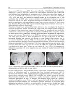
Capacitive microphones generally consist of a diaphragm that is caused to vibrate by
impinging waves of acoustic pressure, a back plate and air gap. In its simplest form, a
diaphragm is stretched over a conductive back plate and supported by post so that there is a
gap between the membrane and the back plate. Figure 1 shows the basic structure of the
condenser microphone. A diaphragm is stretched by a tensile force, T, is put in front of a
fixed conducting back plate by means of a surrounding border which assures a separation
distance, d, to create a capacitance with respect to the back plate and biased with a DC
voltage. An acoustic wave striking the diaphragm causes its flexural vibration and changes
the average distance from the back plate. The change of distance will produce a change in
capacitance and charge, giving rise to a time varying voltage, V, on the electrodes.
This structure works as a condenser whose static capacitance is (Pappalardo et al. 2002):
0
A
C
d
(1)
where ε
0
is the dielectric constant of the air and A is the surface area of the metallized
membrane.
Fig. 1. Basic structure of the condenser microphone
When a DC voltage V
DC
is applied between the two electrodes, an electric charge Q
DV
=
C
0
V
DC
appears on the surface of the membrane, where
0
0
()
DC
A
C
dx
(2)
accounting for the gap height variation due to the bias voltage, and x
DC
is the static average
displacement due to the DC electrostatic force. In reception, an acoustic wave striking the
Design and Fabrication of a Novel MEMS Silicon Microphone
315
membrane causes its flexural vibration and changes the average distance from the back
plate, which becomes
0DC ac ac
xdx x d x
(3)
where
x
ac
is the dynamic average displacement of the vibrating membrane. As a
consequence, the change of distance will produce a change in capacitance and charge, giving
rise to a time varying voltage
V on the electrodes.
0
.
.
QQx
V
CA
(4)
In the small signal approximation, using first order Taylor expansion around the bias point
(
V
DC
; d
0
) we have,
0
00
DC
ac ac ac ac ac
bias
bias
dQ
VV
VQxQx
QxAA
(5)
Where V
ac
and Q
ac
are voltage and charge signal components and Q
DC
the polarization
charge. For this reason the surface electrical charges are forced to move giving rise to a small
alternating current which flows in the pre-amplifier input resistance Z
ia
, through the
condenser C.
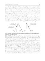
In this research, 2 types of MEMS capacitive microphone have designed and fabricated on 4
inches silicon wafer. First design is microphone with clamped perforated diaphragm (see
Fig. 2). The novelty of this method relies on diaphragm includes some acoustic holes to
reduce air damping in the gap. Compared with previous works, the chip size of this
microphone is reduced; the complex and expensive fabrication process can be avoided by
making acoustic holes in diaphragm. Second design is microphone with slotted perforated
diaphragm (see Fig. 3). The novelties of this method relies on the diaphragm includes some
slots to reduce the effect of residual stress and stiffness of diaphragm and also includes
some acoustic holes to reduce air damping in the gap. By this way, the microphone size was
reduced, and the sensitivity was increased.
In next section, the behaviors of the microphones with clamped and slotted perforated
diaphragms are analyzed using the finite element method (FEM).
(a) (b)
Fig. 2. (a) Cross-section, and (b) top view of clamped perforated microphone (Ganji and
Majlis 2009)
Back plate
electrode
Diaphragm
Air
g
ap
Holes
Crystalline Silicon – Properties and Uses
316
(a) (b)
Fig. 3. (a) Cross-section, and (b) top view of slotted perforated microphone (Ganji and Majlis
2009)
3. Finite element analysis (FEA) of the microphone
The analysis objectives are:
1. To verify the deformation of the diaphragm due to the electrostatic attraction force
between the diaphragm and backplate, and the mechanically applied force
2. To verify the capacitance between the diaphragm and the back plate
The analysis options are nonlinear analysis, accuracy of convergence that is 0.001 µm, and a
maximum mesh size that is 2.4% of X-Y dimension. Figure 4a shows the simulation setup of
the microphone with clamped diaphragm. Silicon wafer faces and 4 lateral faces of the poly
silicon diaphragm are fixed. Figure 4b shows the simulation setup for the microphone with
slotted diaphragm. Silicon wafer faces and 8 lateral faces of arms are fixed. A DC bias
voltage is provided between the diaphragm and the back plate.
Figure 5 show the stress distribution over of the clamped diaphragm (Fig. 5a) and the
slotted diaphragm (Fig. 5b) using the FEM. We can see that the stress concentration is found
at the edges of the clamped diaphragm. For the slotted diaphragm, however, the value of
stress at the center and edges of the diaphragm is very low and it increases as it goes to the
suspending area.
Figure 6 shows deformation in the
Z axis of the diaphragm with a thickness of 3 µm and an
initial stress of 20 Mpa at an applied pressure of 1.5 kPa. Figure 6a shows the maximum
central deflection of clamped diaphragm is 0.245 µm and Figure 6b shows the maximum
deflection of slotted diaphragm is 0.6643 µm. We can see that the slotted diaphragm has
more deflection than the clamped one under same load.
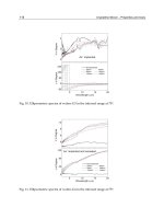
Figure 7 shows the simulated diaphragm deflection versus voltage and Figure 8 show the
simulated diaphragm deflection versus pressure for the clamped diaphragm (2.43 x 2.43
mm
2
) and the slotted diaphragm (1.5 x 1.5 mm
2
). According to the results, both microphones
have the same pull-in voltage (7 V) and the same high mechanical sensitivity (53.3 nm/Pa),
however the slotted microphone is at least 1.62 times smaller than the clamped structure.
Figure 9 shows the central deflection versus bias voltage of the clamped and slotted
microphones using a 0.5-mm square diaphragm with a thickness of 3 µm, an air gap of 1 µm,
and a diaphragm stress of 1500 MPa (Ganji and Majlis 2009). We can see that the pull-in
voltage for the clamped diaphragm is 105 V, and that for the slotted diaphragm is 49 V. We
can see that, by introducing slots in microphone, the diaphragm stiffness decreased,
therefore the pull-in voltage decreased about 53%.
Slots
Design and Fabrication of a Novel MEMS Silicon Microphone
317
(a)
(b)
Fig. 4. Simulation setup for (a) clamped microphone, (b) slotted microphone
Sound pressure
Sound pressure
Fixed
Fixed
V
DC
V
DC
Crystalline Silicon – Properties and Uses
318
(a)
(b)
Fig. 5. Stress distribution on the (a) clamped diaphragm and (b) slotted diaphragm
Design and Fabrication of a Novel MEMS Silicon Microphone
319
(a)
(b)
Fig. 6. Diaphragm deformation on the
Z axis of the (a) clamped diaphragm and (b) slotted
diaphragm
Crystalline Silicon – Properties and Uses
320
0 1 2 3 4 5 6 7 8
0
0.5
1
1.5
2
2.5
3
3.5
4
Deflection (um)
Bais voltage (V)
clamped diaphragm
slottted diaphragm
Fig. 7. Diaphragm deflection versus voltage
0 5 10 15 20 25 30 35 40 45 50
0
0.5
1
1.5
2
2.5
3
Deflection (um)
Pressure (Pa)
clamped diaphragm
slotted diaphragm
Fig. 8. Diaphragm deflection versus pressure
Figure 10 shows the relation between capacitance and pressure for clamped and slotted
microphones under 60% of pull-in voltage. The results yield a sensitivity (
S=dC/dP) of
5.33x10
−6
pF/Pa for the clamped and 3.87x10
−5
pF/Pa for the slotted microphones. By
introducing the slots in the diaphragm, the sensitivity’s increased 7.27 times. The first
resonance frequency of the diaphragm is 1.11 MHz for the clamped and 528.57 kHz for the
Design and Fabrication of a Novel MEMS Silicon Microphone
321
slotted microphones. From the preceding analysis, we can conclude that there is a dilemma
between the high sensitivity and high resonance frequency. For all the diaphragms, to
satisfy most of the microphones, the first resonance frequency of the diaphragm should be
well above 20 kHz (hearing range).
0 20 40 60 80 100 120
0
0.1
0.2
0.3
0.4
0.5
0.6
0.7
0.8
0.9
1
Deflection (um)
Bias voltage (V)
(a)
(b)
Fig. 9. Central deflection of a (curve a) clamped and (curve b) slotted diaphragm versus bias
voltage
0 0.2 0.4 0.6 0.8 1 1.2 1.4 1.6 1.8 2
x 10
4
2
2.1
2.2
2.3
2.4
2.5
2.6
2.7
2.8
Capacitance (pF)
Pressure (Pa)
(b)
(a)
Fig. 10. Capacitance versus pressure for (a) the clamped and (b) the slotted microphones
Crystalline Silicon – Properties and Uses
322
4. Fabrication of microphone
This section will describe how the microphone was fabricated on silicon wafer. In this
process, sputtered aluminum is used as a diaphragm and back plate electrode, resist
(AZ1500) as a sacrificial layer, and sputtered silicon oxide as an insulation layer. The whole
process sequence uses three masks and several deposition, and etching processes. The
process starts with a single side polished silicon wafer as a substrate. The major fabrication
steps are shown in Figure 11, and described as follows:
First a 4-inch silicon wafer should be cleaned using standard cleaning procedure to remove
organic contaminants such as dust particles, grease or silica gel and then remove any oxide
layer from the wafer surface prior to processing. The first step in the cleaning process is to
clean the wafer using ultrasonic in the acetone solution for 5 minutes. The second step is to
put the wafer into the methanol solution using ultrasonic for 5 minutes. Final step is to dip
the sample in a 10:1 DI water-HF solution (10% HF) until hydrophobic (i.e. no water can
stick to wafer). This will remove native oxide film (see Fig. 11a).
Then a 2 µm thick silicon oxide is sputtered on clean silicon wafer as an insulation layer (see
Fig. 11b). Next, a 0.5 µm Al has been sputtered on silicon oxide as a back plate electrode. It
was then patterned using photoresist mask and etched by Al etchant for 5 minutes (see Fig.
11c). The etch rate of sputtered Al in Al etchant is 60 nm/minute. Etchant for aluminum is
16:4:1 of phosphoric acid (H
3
PO
4
), DI water, and nitric acid (HNO
3
). After that, a 1.3 μm
thick resist (AZ1500) was deposited and patterned in order to form a sacrificial layer (see
Fig. 11d). Resist can be easily deposited and removed using acetone. Moreover, acetone has
a high selectivity to resist compared to silicon oxide and Al, thus it completely removes
sacrificial resist without incurring significant damage silicon oxide and Al. Sacrificial resist
is usually deposited by spin coater. Baking is the most important. The main purpose of
baking is to remove solvent from resist. A few minutes of hot plate baking temperature of at
least 100
C is required to evaporate the solvent. The samples are then heated at145
C for 3
minutes.
Then, a 3
m thick layer of aluminum is sputtered on resist sacrificial layer as a material of
diaphragm (see Fig. 11e). The Al layer is then patterned using positive resist mask to define
the geometry of the diaphragm, contact pad, and anchors. After that the structure was
immersed in Al etchant for 35 minutes to etch the Al for making diaphragm structure. The
approximate etch rate of Al in acetone in room temperature is zero. Therefore acetone shows
a high selectivity against Al.
Finally, the sacrificial resist layer is etched using acetone to release the diaphragm (see Fig.
11f). The fabrication process is completed by immersing it in deionized water (DI) and then
acetone. Next, the whole structure is dried on hot plate at 60
C for 90 seconds to protect the
diaphragm from sticking to the back plate.
After all processing on the wafers were completed, the last step was to determine if the
fabrication process had been successful. It is important to observe the silicon membrane and
check to ensure that the resist layer was removed. All testing was performed by using a
Scanning Electron Microscope (SEM) and optical microscope to capture images of the
membrane surface and images of the cross-section. Figure 12 shows the optical microscopy
top view of Al back plate electrode and photoresist (AZ1500) sacrificial layer on silicon
oxide.
Design and Fabrication of a Novel MEMS Silicon Microphone
323
Figure 13(a) shows the surface of the fabricated clamped microphone and Figure 13(b)
shows the close up view of the Al diaphragm surface (0.5x0.5 mm
2
) with acoustic holes
using SEM. Figure 14 shows the SEM image of slotted microphone with 8 slots and 8 arms.
Figure 15 show the sacrificial layer etching with diaphragm thickness of 3μm, and air gap of
1.3μm. It can be seen that, sacrificial layer has been removed under Al membrane
completely, and Al membrane has been released.
The measured pull-in voltage for clamped microphone is 51 V, however the measured pull-
in voltage of slotted microphone with sputtered aluminum diaphragm is 25 V. It can be seen
that, by introducing slots in microphone, the diaphragm stiffness decreased, therefore the
pull-in voltage about 50% decreased. Consequently, it causes the microphone sensitivity is
increased.
Si
(a) (b)
(c) (d)
(e) (f)
Fig. 11. Process flow of the microphone (Ganji and Majlis 2010)
Crystalline Silicon – Properties and Uses
324
Fig. 12. Top view of Al back plate electrode and photoresist sacrificial layer on silicon
oxide
(a) (b)
Fig. 13. (a) Surface of the clamped microphone, (b) close up view of the diaphragm
Diaphragm
contact pad
Back plate
contact pad
Clamped
diaphragm
Al electrode
Resist sacrificial
layer
Design and Fabrication of a Novel MEMS Silicon Microphone
325
(a) (b)
Fig. 14. SEM picture of (a) slotted microphone, (b) close up view of diaphragm
(a) Air gap of microphone (b) Released membrane structure
Fig. 15. Cross-section view of the microphone structure using SEM machine (Ganji and
Majlis 2009)
5. Test of microphone
Figure 16 shows the MEMS capacitive microphone has been connected to amplifier,
power amplifier and speaker. The bias voltage of microphone, V
b
, is 3 V, and bias
resistance, R
b
, is 100MΩ. The amplifier consists of an operational amplifier LF347 with
high input impedance of 10
12
Ω, R
f
of 1 MΩ, R
s
of 1.25 KΩ, and Vcc of 9 V battery. The
voltage gain of amplifier, (A
v1
= R
f
/R
s
) is 800. The power amplifier is a mini amplifier-
speaker CAT. No. 277-1008C. The voltage gain of power amplifier, A
v2
, is 50. The total
voltage gain of external amplifier, (A
vtot
= A
v1
.A
v2
) is 40000. Figure 17 shows the 2 seconds
of a speech signals are applied to the microphone. It can be seen that the external
amplifier was able to detect the sound waves from microphone on oscilloscope. From the
figure, the maximum amplitude of output speech signal of amplifier is 45 mV, thus the
maximum output of microphone is 1.125 µV.
Back plate
Air gap
Al diaphragm
Released membrane
Crystalline Silicon – Properties and Uses
326
Fig. 16. Circuit diagram of external amplifier which connected to microphone (Ganji and
Majlis 2010)
-1 -0.8 -0.6 -0.4 -0.2 0 0.2 0.4 0.6 0.8 1
0.01
0.02
0.03
0.04
0.05
0.06
0.07
0.08
0.09
0.1
Time (s)
Amplitude (V)
Speach signals
Noise
Fig. 17. 2 seconds of speech signals are applied to the microphone
6. Conclusion
A novel MEMS capacitive microphone was designed, and fabricated with a small size and a
high sensitivity. The device used a perforated diaphragm, mono crystalline silicon back
plate, and resist as a sacrificial layer. The results show the obvious improvement in size and
sensitivity of the slotted microphone compared with the clamped one. According to the
results, the slotted microphone with a 1.5-mm diaphragm width, at least 1.62 times is
smaller than the clamped structure with a 2.43-mm diaphragm width. The results also yield
a sensitivity of 5.33 x10
−6
pF/Pa for the clamped and 3.87 x10
−5
pF/Pa for the slotted
Design and Fabrication of a Novel MEMS Silicon Microphone
327
microphones using a 0.5-mm square aluminum diaphragm with a thickness of 3 µm and an
air gap of 1 µm. We can see that, by introducing the slots in the diaphragm, the microphone
sensitivity was increased 7.27 times. The measured pull-in voltage for the clamped
microphone with sputtered aluminum diaphragm is 51 V, however, the pull-in voltage of
the slotted microphone is 25 V. This means that the slotted diaphragm stiffness has been
decreased; consequently, the pull-in voltage decreased about 50%. The microphone has been
tested with external amplifier and speaker, it can be seen that the external amplifier was able
to detect the sound waves from microphone on speaker. The maximum amplitude of output
speech signal of amplifier is 45 mV, and the maximum output of microphone is 1.125 µV.
7. References
Bergqvist, J., Gobet, J. (1994). Capacitive microphone with a surface micromachined
backplate using electroplating technology.
J. Microelectromech. Syst. 3(2): 69–75.
Chowdhury, S., Jullien, G. A., Ahmadi, M. A., Miller, W. C. (2000). MEMS acousto-magnetic
components for use in a hearing instrument.
Presented at SPIE’s Symposium on
Design, Test Integration, and Packaging of MEMS/MOEMS, Paris
.
Ganji, B. A. and Majlis, B. Y. (2009). Design and fabrication of a new MEMS capacitive
microphone using a perforated aluminum diaphragm.
Sensors and Actuators A:
Physical, 149: 29–37.
Ganji, B. A. and Majlis, B. Y. (2009). Design and fabrication of a novel single-chip MEMS
capacitive microphone using slotted diaphragm.
J. Micro/Nanolith. MEMS MOEMS
8(2), DOI: 10.1117/1.3091941, pp.021112 (1-7).
Ganji, B. A. and Majlis, B. Y. (2009). Fabrication and Characterization of a New MEMS
Capacitive Microphone using Perforated Diaphragm.
International journal of
Engineering,
Vol. 22, No. 2, pp. 153-160.
Ganji, B. A. and Majlis, B. Y. (2009). High Sensitivity and Small Size MEMS Capacitive
Microphone using a Novel Slotted Diaphragm,
Microsystem Technology, Vol. 15,
Issue 9, pp: 1401-1406.
Ganji, B. A. and Majlis, B. Y. (2010). Slotted capacitive microphone with sputtered aluminum
diaphragm and photoresist sacrificial layer, Microsystem Technology, Vol. 16, pp:
1803–1809.
Hsu, P. C., Mastrangelo, C. H., Wise, K. D. (1988). A high density polysilicon
diaphragmcondenser microphone.
In Conf. Record IEEE 11th Int. Workshop on
MicroElectro Mechanical Systems (MEMS)
, pp. 580–585.
Jing, C., Liu, L., Li, Z., Tan, Z., Xu, Y., Ma, J. (2003). On the single-chip condenser miniature
microphone using DRIE and back side etching techniques.
Sens. Actuators, A 103:
42–47.
Kabir, A. E. , Bashir, R., Bernstein, J., De Santis, J., Mathews, R., O’Boyle, J. O., Bracken, C.
(1999) Very High Sensitivity Acoustic Transducers with Thin P
+
Membrane and
Gold Back Plate
Sensors and Actuators-A, 78: 138-142.
Kronast, W., Muller, B., Siedel, W., Stoffel, A., (2001). Single-chip condenser microphone
using porous silicon as sacrificial layer for the air gap. Sens. Actuators, A 87: 188–
193.
Li, X., Lin, R., Kek, H., Miao, J., Zou, Q. (2001). Sensitivity- improved silicon condenser
microphone with a novel single deeply corrugated diaphragm.
Sensors and
Actuators
A 92: 257-262.
Crystalline Silicon – Properties and Uses
328
Ma, T., Man, T.Y., Chan, Y. C., Zohar, Y., Wong, M. (2002). Design and fabrication of an
integrated programmable floating-gate microphone.
Proceedings of the Fifteenth IEEE
International Conference on Micro Electro Mechanical Systems
, pp. 288–291.
Miao, J., Lin, R., Chen, L., Zou, Q., Lim, S. Y., Seah, S. H. (2002). Design considerations in
micromachined silicon microphones.
Microelectronics Journal 33: 21-28.
Ning, J., Liu, Z., Liu, H., Ge, Y. (2004). A silicon capacitive microphone based on oxidized
porous silicon sacrificial technology.
Proc. 7
th
Int. Conf. on Solid-State and Integrated
Circuits Technology,
IEEE, 3: 1872–1875.
Ning, Y. B., Mitchell, A. W., Tait, R. N. (1996). Fabrication of a silicon micromachined
capacitive microphone using a dry-etch process.
Sens. Actuators, A 53: 237–242.
Pappalardo, M, Caliano, G, Foglietti, V, Caronti, A, Cianci, E (2002) A new approach to
ultrasound generation: the capacitive micromachined transducers.
University Roma,
Rome, Italy
.
Pappalardo, M., A. Caronti (2002). A new alternative to piezoelectric transducer for NDE
and medical applications: the capacitive ultrasonic micromachined transducer
(cMUT).
University Roma, Rome, Italy.
Pedersen, M., Olthuis, W., Bergveld, P. (1997). A silicon condenser microphone with
polyimide diaphragm and back plate. Sens. Actuators, A 63: 97–104.
Rombach, P., Mullenborn, M., Klein, U., Rasmussen, K. (2002). The first low voltage, low
noise differential silicon microphone, technology development and measurement
results.
Sens. Actuators, A 95: 196– 201.
Torkkeli, A., Rusanen, O., Saarilahti, J., Seppa, H., Sipola, H., Hietanen, J. (2000). Capacitive
microphone with low- stress polysilicon membrane and high-stress polysilicon
backplate.
Sens. Actuators 85: 116–123.
15
Global Flow Analysis of Crystalline Silicon
Hiroaki Takiguchi
1
and Kazuki Morita
2
1
Ministry of the Environment
2
The University of Tokyo
Japan
1. Introduction
Silicon is a unique material. Next to oxygen, it is the second most abundant element in the
Earth’s crust. Its abundance is one of the reasons it is used for a wide range of purposes.
One of the most important uses of silicon is as a core element of microchips. To
manufacture microchips, the microelectronics industry requires silicon with an impurity
level of 10
–11
. Since silicon forms a stable compound with oxygen (silicon oxide, SiO
2
), the
deoxidization of silicon oxide needed to reach this high level of purity consumes a
substantial amount of energy, which, in turn, affects the environment through emissions of
carbon dioxide (CO
2
).
In the past decade, there has been a dramatic increase in the global supply and demand of
crystalline silicon. This is because of a drastic increase in the demand for crystalline silicon
for photovoltaic (PV) cells. While a core element for renewable energy, the purification
process of crystalline silicon is energy-intensive. Therefore, the sustainability of crystalline
silicon feedstock is an interesting area for research. The effective use of crystalline silicon
could contribute to the sustainability of global environmental systems.
Reflecting its importance to sustainability, there has been a growing literature on material
flows of crystalline silicon. Some studies highlight energy use and environmental impacts
in the process of crystalline silicon production. For instance, Williams conducted a
quantitative systems analysis of global production chains for silicon (Williams, 2003). He
estimated global material flows of silicon in 1998 and then forecast how these flows would
project out to 2020. In analyzing material flows, he chose different physical units such as
weight and area, according to the characteristics of different outputs. Using this approach,
Williams et al. were able to determine the energy required for a microchip based on the
calculation on energy use at each production stage (Williams et al., 2002). Their analysis
further was able to show in a quantitative manner that the purification to electronic grade
silicon (EG-Si) is an energy intensive process.
Other studies have focused on the supply of crystalline silicon for solar cells. Woditsch and
Koch expressed concern about the shortage of crystalline silicon for solar cells which were
dependent on off-grade silicon from the EG-Si production process (Woditsch & Koch, 2002).
They concluded that new routes for solar-grade silicon production are urgently needed.
Sarti and Einhaus proposed short- and long-term solutions to respond to the demand for
polycrystalline silicon (pc-Si, also called multicrystalline silicon) for solar cells. Their
recommendations included a reduction in the amount of crystalline silicon in the short-term
Crystalline Silicon – Properties and Uses
330
and the establishment of solar-grade silicon production from metallurgical-grade silicon
(MG-Si) (Sarti & Einhaus, 2002).
As for major metals such as iron, copper and nickel, the Yale Stocks and Flows project
conducted a material flow analysis of substances on national, regional and global scales (for
example, Graedel et al., 2004). Their approach focused on illustrating anthropogenic metal
cycles through four processes: production, fabrication and manufacturing, use and waste
management. They then offered useful suggestions on the benefits and challenges of a
material flow analysis.
In a previous paper, Takiguchi and Morita presented a material flow analysis of silicon in
Japan from 1996 to 2006 (Takiguchi & Morita, 2009). The analysis tracked the input and
output of silicon in a series of purification process in units of weight and found that rapid
growth in demand for pc-Si and single crystalline silicon (sc-Si, also called monocrystalline
silicon) changed the structure of the crystalline silicon supply. Takiguchi and Morita also
developed the Resource Effective-use Index (REI) to demonstrate how effectively crystalline
silicon is used. The analysis of the REI indicated that the effective use of pc-Si had reached
its outer limits. At the same time, the paper found a domestic analysis was limited in what
it could demonstrate because crystalline silicon is traded globally.
This chapter analyzes and discusses the global flow of crystalline silicon to assess the
sustainability of silicon feedstock. The chapter begins by reviewing how crystalline silicon
is produced as well as recent trends in crystalline silicon supply. The next section provides
a material flow analysis of silicon on a global scale, focusing mainly on crystalline silicon for
solar cells. The “results and discussion” section describes the results of the material flow
analysis, followed by a discussion of the sustainability of silicon feedstock.
2. Crystalline silicon and solar cells
Before conducting a material flow analysis, this section observes the recent trend of solar cell
production and explains how crystalline silicon is produced, followed by sources of
crystalline silicon for solar cells.
2.1 Expansion of solar cell production
Nowadays, many countries have promoted the use of renewable energy to reduce carbon
dioxide (CO
2
) for climate change mitigation and diversify energy sources. In particular, the
installation of PV systems is expanding in many parts of the world. Under these
circumstances, the production of solar cells, core elements of PV systems, is increasing rapidly.
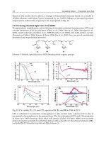
Fig. 1 illustrates trends in solar cells production by types. The total production of solar cells
in the world sharply increased from 126 MW in 1997 to 10,660 MW in 2009. The share of sc-
and pc- Si solar cells grew the most at 32% and 45%, respectively. This can be attributed to
the ease of mass production using highly developed silicon technology, a good balance
between energy conversion efficiency and cost, and the fact that their products are non-
toxic. These advantages suggest that crystalline silicon (pc- and sc- Si) solar cells will be
likely to continue to expand in the future.
2.2 Process for crystalline silicon production
A typical production process for crystalline silicon for semiconductors is illustrated in Fig. 2.
In the first step, the reduction of silica (quartz, SiO
2
) produces metallurgical-grade silicon
(MG-Si) with a purity of approximately 98% in electronic furnaces.
Global Flow Analysis of Crystalline Silicon
331
Fig. 1. Trends in solar cell production by types.
The second step is purification from MG-Si to pc-Si. Usually, a chemical gaseous
purification technique known as the Siemens method is used for purification. This method
involves reacting MG-Si with hydrochloric acid (HCl) to convert purified trichlorosilane
(SiHCl
3
) by distillation (Si + 3HCl SiHCl
3
+ H
2
). The trichlorosilane is then decomposed
with hydrogen on pure silicon surfaces and converted back into pc-Si (SiHCl
3
+ H
2
Si +
3HCl). After the reaction, pc-Si with an impurity level of 10
–11
is obtained. In this process,
the formation of silicon tetrachloride (SiCl
4
) as a by-product of the production of
trichlorosilane lowers the yield of pc-Si.
Quartz (SiO
2
)
Metallurgical-grade
silicon (MG-Si)
Polycrystalline silicon
(pc-Si)
Single crystalline
silicon (sc-Si)
Wafer
Deoxidization
Siemens Method
Czochralski Method
Fig. 2. Typical process flow for purified Si production.
Crystalline Silicon – Properties and Uses
332
The third step is to convert pc-Si to sc-Si. For the conversion process, the semiconductor
industry usually employs the Czochralski (CZ) method. In the CZ method, sc-Si grows on a
seed crystal drawn up from molten pc-Si in a crucible, producing a sc-Si ingot. The
cylindrical ingot of sc-Si is sliced into wafers followed by a series of processes such as
wrapping and etching. Finally, the wafers are processed into integrated circuit (IC) chips.
Table 1 provides the energy consumption at each stage from quartz to wafers (Frankl etc.,
2004). It is obvious that the process of producing pc-Si from MG-Si consumes the most energy
of all of the processes. While it is the established and most frequently used method of
producing pc-Si, the production method presents several issues that need to be resolved, such
as the limited velocity of the chemical reaction, the considerable initial investment required to
enlarge the process, and the high cost in proportion to high consumption of energy.
Product
Electrical energy
input/ kg silicon out
(kWh/kg)
Silicon
yield
Quartz
→
MG- Si 11 0.79
MG-Si
→
pc-Si 149.9 0.76
pc-Si
→
sc-Si ingot
(Czochralski)
31.1 1
sc-Si ingot
→
wafer 42.5 0.37
Table 1. Energy required for Si purification.
2.3 Crystalline silicon for solar cells
Crystalline silicon for solar cells does not require a purity level as high as the level required for
semiconductors. While the impurity level required for EG-Si is 10
-11
, the level for pc-Si solar
cells is 10
-7
to 10
-6
. Therefore, off-grade silicon produced as a by-product of the EG-Si
production process has been used for solar cells. The following describes the process typically
used to generate off-grade silicon. In the process of crushing pc-Si, approximately 5-10% of the
produced pc-Si is lost; this is used as off-grade silicon. In the CZ process of producing sc-Si,
nearly 40% of the pc-Si is lost as pot scrap, tops and tails, kerf loss and test wafers (Fig. 3) and
used as off-grade silicon (New Energy and Industrial Technology Development Organization
[NEDO], 2001). Scrap wafers are also used as off-grade silicon. The off-grade silicon is melted
and turned into a pc-Si ingot via castings in a crucible mold or a sc-Si ingot via another CZ
process. Polycrystalline silicon or sc-Si produced from the off-grade silicon ingot is sliced into
wafers with a wire saw and used for solar cells. Depending on its purity level, off-grade
silicon is used for other low-grade purposes such as making aluminium alloy.
In the 1990s, off-grade silicon obtained from the EG-Si production process satisfied the
demand for silicon for solar cells. The recent increase in demand for solar cells, however,
resulted in production of crystalline silicon independently, not as scraps of EG-Si. Since the
purification level of pc-Si for solar cells is lower than that for semiconductors, pc-Si for solar
cells is produced by a simplified Siemens method which increases the speed of
trichlorosilane decomposition. It should be noted that the simplified method still consumes
considerable energy.
Thus, crystalline silicon for solar cells is currently obtained from two sources: 1) off-grade
silicon produced as a by-product of the EG-Si production process and 2) silicon produced
independently for solar cells.
Global Flow Analysis of Crystalline Silicon
333
Top
Tail
Test wafer
Test wafer
Products
Sample
Kerf
loss
Pot scrap
poly-crystalline Si 100%
Products
Prime wafer 55~65%
Test wafer 10~15%
(Dummy & monitor)
Off-grade
Top & tail 10~15%
Pot scrap ~10%
Sample & Kerf loss ~5%
Fig. 3. Products and off-grade crystalline Si of Czochralski (CZ) ingot.
3. Global flow analysis of crystalline silicon
This section presents a material flow analysis of crystalline silicon. After explaining the
scope and methodology of the analysis, the material flows are shown and discussed.
3.1 Scope of material flow analysis
A material flow analysis tracks flows of materials at a particular scale in a quantitative
manner. Possible scales include the global, regional, national, community, or factory scale.
A material flow analysis for a specific material is called a “substance flow analysis.” This
chapter analyzes the material flow of crystalline silicon, clarifying the input and output of
the material at each phase of the production process.
In undertaking a material flow analysis, the scope of the material flow should be clarified.
This chapter analyzes the material flow of silicon on a global scale from 1997 to 2009. The
material flow also focuses on the stages of production, fabrication and manufacture (Fig.4),
because it aims to demonstrate the sustainable supply of crystalline silicon. The global scale
was chosen as the geographical boundary for the material flow analysis since the objective
of this analysis is to understand the sustainability of flows. Nowadays, material flows at the
national level would not be closed due to the export and import of the materials. A global
material flow can offset export and import and hence capture the entire flows. On the other
hand, a drawback of the global material flow is the quality of data. A global material flow
requires global data. While some countries have robust data, others do not, which can
influence the accuracy of the analysis. Therefore, these advantages and disadvantages
should be considered carefully in analyzing global material flows.
Crystalline Silicon – Properties and Uses
334
The timeframe for the material flow analysis is 1997 to 2009. This twelve year period starts
when relevant solar cell first became available and goes to the latest available data. Whereas
a material flow in a single year is like a “snapshot,” a time series analysis of material flows
over the period enable illustrates the changes of flows over time.
In the material flow analysis in this chapter, silicon used for making thin-film and
amorphous types are not considered, because silicon used for these types seems to be less
than 1% of that used for making the crystalline types. This point is discussed in greater
detail in the “results and discussion” section.
3.2 Methodology
To determine the material flow of silicon on a global scale, data used for the analysis and the
respective sources are listed in the Table 2. The assumptions made in developing the
material flow and methodologies to estimate values are based mainly on Takiguchi and
Morita (Takiguchi & Morita, 2009). Most of the data for the material flows are gathered
from the Japanese journal Industrial Rare Metal, which reviews annual trends in industrial
materials (Industrial Rare Metal, 1998-2010).
Wafer Fabirication
Si Purification
EG sc-Si (P
sc, e
)
EG pc-Si (P
pc, e
)
Casting
pc-Si solar
cell (D
pc,s
)
CZ
Process
sc-Si solar cell
(D
sc,s
)
Wafers (P
w
)
CZ Process
pc-Si for solar
cells (P
pc,s
)
Off-grade pc-Si for
solar cells (O
pc,s
)
Off-grade sc-Si for
solar cells (O
sc,s
)
MG-Si (P
mg
)
Other Use
Wafer
Production
Quartz
sc-Si for solar cells (P
sc,s
)
Input
Output
CZ Process
Fig. 4. Analyzed process flow of Si production.
Global Flow Analysis of Crystalline Silicon
335
Product Category Symbol Method References
MG-Si Production P
mg
Primary Industrial Rare Metal
pc-silicon EG Production P
pc, e
Primary Industrial Rare Metal
Production for solar cells P
pc, s
Primary Industrial Rare Metal
Off-grade for solar cells O
pc,s
Not available -
Demand for solar cells D
pc,s
Estimated Prometheus Institute
sc-silicon EG production P
sc, e
Estimated Industrial Rare Metal
Production for solar cells P
sc, s
Not available -
Off-grade for solar cells O
sc, s
Not available -
Demand for solar cells D
sc, s
Estimated Prometheus Institute
Wafer Production P
w
Primary and Estimated SEMI
Table 2. Data sources and calculation methods.
3.2.1 Metallurgical-grade silicon
MG-Si is supplied mainly by China, Norway, and Brazil with China increasingly recognized
as the dominant supplier. MG-Si is used for various purposes: production of crystalline
silicon; deoxidization of steel; and production of aluminium alloy and silicon resin etc. Data
on the supply of MG-Si on a global scale are available (Industrial Rare Metal, 1997-2010). It
is assumed that the supply of MG-Si is equal to the figures in that data. While data
regarding the amount of MG-Si used for crystalline silicon were not available, it is estimated
that nearly 1.3 kg MG-Si is used to produce 1 kg pc-Si.
3.2.2 Polycrystalline silicon
Polycrystalline silicon as the primary products is divided into electronic-grade pc-Si (EG
pc-Si, P
pc,e
) and pc-Si produced independently for solar cells (P
pc,s
). Data on the
production of P
pc,e
and P
pc,s
are available (Industrial Rare Metal, 1998-2010). In 2009,
92,100 tons of pc-Si was produced, the ratio of P
pc,s
to P
pc,e
being approximately 3:1. The
data are the sum of production by manufacturers located mainly in the United States,
Japan and Germany. Off-grade pc-Si (O
pc
) is generated in the pc-Si production process
and the CZ process.
The total demand for pc-Si for solar cells (D
pc,s
) is satisfied by two sources: off-grade
pc-Si for solar cells (O
pc,s
) and pc-Si produced independently for solar cells (P
pc,s
). Based on
the assumption that there is no loss in casting, this supply and demand relationship is
expressed as:
P
pc,s
+ O
pc,s
= D
pc,s
(1)
Because pc-Si (P
pc,s
) has been produced independently for solar cells since around 2000, the
chapter assumes that P
pc,s
was zero before the year 2000. Demand for pc-Si for solar cells
(D
pc,s
) has been calculated by multiplying the global production of pc-Si solar cells (in Watts)
by the amount of pc-Si used for the production of 1 W. Since the amount of pc-Si consumed
per Watt steadily decreased from 20 g in 1995 to 15 g in 2000 to 10 g in 2005 (Industrial Rare
Crystalline Silicon – Properties and Uses
336
Metal), it is estimated from this linear relationship from 1997-2005. After 2006, it is
estimated at 9 g per Watt.
It should be noted that there is a loss of crystalline silicon in the wafer saw process. Given
15% for the cell efficiency and 180 micrometers for the wafer thickness, 1 W of the solar cell
includes 2.8 g of pc-Si inside. The difference between the demand of pc-Si for solar cells (9
g/W in 2009) and 2.8 g is the loss.
Although the amount of off-grade pc-Si for solar cells is not given, it can be estimated by
equation (1). Data for the average price of EG pc-Si per ton each year was available
(Industrial Rare Metal, 1998-2010).
3.2.3 Single crystalline silicon
Single crystalline silicon as the primary product is divided into EG sc-Si (P
sc,e
) and sc-Si
produced independently for solar cells (P
sc,s
). While data on these variants of silicon are not
available, EG sc-Si can be estimated by multiplying the amount of EG pc-Si (P
pc,e
) by the
yield rate of EG sc-Si. In this chapter, the rate was set at 0.7. Single crystalline silicon is
produced independently for solar cells, partly using pc-Si for solar cells. Off-grade sc-Si
(O
sc
) is generated in the wafer production process or as wafer waste and presumably used
for solar cells. Data on the off-grade sc-Si are also not available. As well as pc-Si for solar
cells, off-grade sc-Si was used as a proxy for the demand for sc-Si for solar cells until around
the year 2000.
The same approach to estimating the demand of pc-Si for solar cells (D
pc,s
) is applied to
estimating demand of sc-Si for solar cells (D
sc,s
), assuming that consumption of sc-Si per
Watt is identical to that of pc-Si for solar cells. The amount of sc-Si per Watt for the
combined type of sc-Si and amorphous silicon in heterostructures was assumed to be 60% of
other sc-Si cells.
3.2.4 Wafers
In Fig. 4, “wafers” refers to those used for semiconductors not solar applications. Data
regarding the global shipments of wafers for semiconductors are available in units of area
(Semiconductor Equipment and Materials International [SEMI], 2011) and are assumed to
be equal to production of the wafers (P
w
). The calculation of weight of the wafers requires
currently unavailable thickness data. Therefore, composition of wafers in diameter has
been assumed to be identical to the case in Japan (Ministry of Economy, Trade and
Industry, Japan, 1997–2010). Using this assumption, the composition of wafers in 2009 is
4.2% for a wafer under 5 inches (in.), 10.4% for 6 in., 22.6% for 8 in., and 62.7% for 12 in.
The weight of products, in turn, has been calculated based on the assumptions that the
density of a wafer is equal to that of silicon (2,330 kg/m
3
) and that the thickness is
0.625 mm for a wafer under 5 in., 0.675 mm for 6 in., 0.725 mm for 8 in., and 0.775 mm for
12 in.
3.2.5 Resource effective-use index
As in Takiguchi and Morita, the chapter uses the resource effective-use index (REI), which is
the ratio of resource input to output required for a given product (Takiguchi & Morita,
2009). The REI enables one to measure quantitatively the extent to which resources are used
effectively. The trend in the REI values, therefore, explains how effectively the materials in
Global Flow Analysis of Crystalline Silicon
337
question have been used over time. The increase of the REI value means that the resource in
question is being used more effectively.
In this chapter, the input is the sum of production of electronic-grade pc-Si (P
pc,e
) and pc-Si
produced independently for solar cells (P
pc,s
), while the output is the sum of demand of pc-
Si and sc-Si for solar cells (D
pc,s
and D
sc,s
) and production of wafers (P
w
). The REI can be
defined as follows:
,,
,,
w
p
cs scs
pc e pc s
PD D
REI
PP
(2)
To be exact, reuse of wafers as off-grade silicon should be added into the inputs in the
calculation of the REI. However, data on the amount of reuse are not available, and
therefore they are excluded.
3.3 Results and discussion
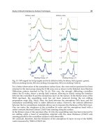
In the period of interest, the amount of crystalline silicon supply has expanded. Fig. 5
illustrates that the growing demand of crystalline silicon for solar cells brought about the
increase in pc-Si supplies. The supply increased from 16,050 tons in 1997 to 92,100 tons in
2009. The production level of wafers decreased in 2009 from the previous year, probably
due to the financial crisis and global economic slump. Nevertheless, it merits attention that
the supply of pc-Si did not decline despite of downward trends in the global economy.
Fig. 5. Production of pc-silicon and wafers.
As Fig. 6 clearly shows, the growing demand for crystalline silicon boosted its price. The
price of pc-Si increased after 2004 and approached nearly 10,000 Japanese Yen (JPY) per kg
(approximately, 100 US dollars, using the exchange rate: 1 US$ = 100 JPY). In 2008 and 2009,
the trend remained stable mainly because of sufficient pc-Si supply.
The main objective of this chapter is to track the material flow of silicon on a global scale.
Figs. 7 and 8 show the global material flows of silicon in 1997 and 2009 respectively.
Crystalline Silicon – Properties and Uses
338
Comparing the two figures, there is a remarkable increase in the amount of silicon at each
stage. The 1997 material flow is relatively simple, because demand for crystalline silicon for
solar cells was covered by the off-grade silicon from the EG-Si production process. In 2009,
however, pc-Si produced independently for solar cells was much larger than the off-grade
silicon.
Fig. 6. Price of pc-silicon.
While the global material flow expanded over the period of interest, the question is how
effectively crystalline silicon had been used. An analysis of trends in the REI can help
answer this question. Fig. 9 describes the trends in the REI. From 2001 to 2008, the values of
REI consistently increased. This trend implies progress in the effective use of crystalline
silicon. In 2009, however, the REI fell to 0.92 from 1.14 in 2008, partly because the global
economic downturn created some slack between supply and demand.
Effective use of crystalline silicon was probably achieved by improvements in the yield rate
at each stage, reductions in wafer thickness and kerf loss, and enhanced use of off-grade
silicon. Off-grade silicon, which was used as a cheap additive to aluminium alloy in the
past, is now used for more valuable products—i.e. solar cells.
It is interesting to note that the REI value exceeded 1.0 in 2008. This implies the mass
balance was not achieved in that year, partly because of the reuse of test wafers, changes in
stocks, and inaccuracy of data. Nevertheless, the upward trend in the REI values is
apparent.
Fig.10 plots the REI values as a function of the price over the period of interest. The REI
values seem to rise in response to the pc-Si’s increasing price, because the increasing value
leads to the more efficient use of materials. This applies to the second half of the analyzed
period. In the first half of the period, the REI values increased despite price fluctuations.
This is not surprising, given the fact that advanced technologies for effective use of pc-Si
would be used regardless of price fluctuations once they were built. According to Tilton,
the supply of scraps generated in the course of producing new goods is unresponsive to
changes in the market price because of the ease of its collection, high quality, and low
recycling cost (Tilton, 1999).