Photodiodes World Activities in 2011 Part 1 pot
Bạn đang xem bản rút gọn của tài liệu. Xem và tải ngay bản đầy đủ của tài liệu tại đây (958.83 KB, 30 trang )
PHOTODIODES - WORLD
ACTIVITIES IN 2011
Edited by Jeong-Woo Park
Photodiodes - World Activities in 2011
Edited by Jeong-Woo Park
Published by InTech
Janeza Trdine 9, 51000 Rijeka, Croatia
Copyright © 2011 InTech
All chapters are Open Access articles distributed under the Creative Commons
Non Commercial Share Alike Attribution 3.0 license, which permits to copy,
distribute, transmit, and adapt the work in any medium, so long as the original
work is properly cited. After this work has been published by InTech, authors
have the right to republish it, in whole or part, in any publication of which they
are the author, and to make other personal use of the work. Any republication,
referencing or personal use of the work must explicitly identify the original source.
Statements and opinions expressed in the chapters are these of the individual contributors
and not necessarily those of the editors or publisher. No responsibility is accepted
for the accuracy of information contained in the published articles. The publisher
assumes no responsibility for any damage or injury to persons or property arising out
of the use of any materials, instructions, methods or ideas contained in the book.
Publishing Process Manager Petra Zobic
Technical Editor Teodora Smiljanic
Cover Designer Jan Hyrat
Image Copyright Shebeko, 2010. Used under license from Shutterstock.com
First published July, 2011
Printed in Croatia
A free online edition of this book is available at www.intechopen.com
Additional hard copies can be obtained from
Photodiodes - World Activities in 2011, Edited by Jeong-Woo Park
p. cm.
ISBN 978-953-307-530-3
free online editions of InTech
Books and Journals can be found at
www.intechopen.com
Contents
Preface IX
Part 1 Generals of Photodetection 1
Chapter 1 An Absolute Radiometer
Based on InP Photodiodes 3
Ana Luz Muñoz Zurita,
Joaquin Campos Acosta and Alicia Pons Aglio
Chapter 2 Physical Principles of Photocurrent Generation
in Multi-Barrier Punch-Through-Structures 23
A.V. Karimov, D.M. Yodgorova and O.A. Abdulkhaev
Chapter 3 Photon Emitting, Absorption and
Reconstruction of Photons 37
Changjun Liao, Zhengjun Wei and Jindong Wang
Part 2 CMOS Related Topics 63
Chapter 4 CMOS Photodetectors 65
Albert H. Titus, Maurice C-K. Cheung
and Vamsy P. Chodavarapu
Chapter 5 Image Artifacts by Charge Pocket in Floating
Diffusion Region on CMOS Image Sensors 101
Sang-Gi Lee, Jong-Min Kim, Sang-Hoon Bae,
Jin-Won Park
and Yoon-Jong Lee
Chapter 6 Active Pixel Sensor CMOS Operating
Multi - Sampled in Time Domain 121
Fernando De Souza Campos
Chapter 7 Bandwidth Extension for
Transimpedance Amplifiers 139
Omidreza Ghasemi
VI Contents
Part 3 APD and Single Photon Detection 157
Chapter 8 Avalanche Photodiodes in
High-Speed Receiver Systems 159
Daniel S. G. Ong and James E. Green
Chapter 9 Silicon Photo Multipliers Detectors
Operating in Geiger Regime: an
Unlimited Device for Future Applications 183
Giancarlo Barbarino, Riccardo de Asmundis, Gianfranca De Rosa,
Carlos Maximiliano Mollo, Stefano Russo and Daniele Vivolo
Chapter 10 Near-Infrared Single-Photon Detection 227
Guang Wu, E Wu, Xiuliang Chen,
Haifeng Pan and Heping Zeng
Chapter 11 Geiger Avalanche Photodiodes
(G-APDs) and Their Characterization 247
Giovanni Bonanno, Massimiliano Belluso,
Sergio Billotta, Paolo Finocchiaro and Alfio Pappalardo
Chapter 12 Design of High Quantum Efficiency and High
Resolution, Si/SiGe Avalanche Photodiode
Focal Plane Arrays Using Novel, Back-Illuminated,
Silicon-on-Sapphire Substrates 267
Alvin G. Stern
Part 4 Extended Topics of Photodiodes 313
Chapter 13 Single Crystal Diamond Schottky Photodiode 315
Claudio Verona
Chapter 14 GaN Based Ultraviolet Photodetectors 333
D. G. Zhao and D. S. Jiang
Chapter 15 Quantum Dot Composite Radiation Detectors 353
Mario Urdaneta, Pavel Stepanov, Irving Weinberg,
Irina Pala and Stephanie Brock
Chapter 16 HgCdTe Heterostructures Grown by
MBE on Si(310) for Infrared Photodetectors 367
Maxim Yakushev, Vasily. Varavin, Vladimir Vasilyev,
Sergey Dvoretsky, Irina Sabinina,Yuri. Sidorov,
Aleksandr Sorochkin and Aleksandr Aseev
Preface
Photodiodes or photodetectors are prevailing technology in various fields giving
many benefits to human race. Moreover, their application fields are extended in the
world more and more. From photo camera application to medical application, they are
pervading in the human life. They became an inevitable and valuable technology since
its birth. Now we cannot imagine what is like our life without them. They would exist
until end of human race even if we don’t need our sight of today anymore. Even
though we become a new race after gradual evolution, we would need suitable
photodiodes and photodetectors. They are in one boat with our human race.
Many people in the world pursuit a birth of new photodiodes or photodetectors
technology which are able to give better life to human. Their efforts are contained in
this book. This book would be valuable to those who want to obtain knowledge and
inspiration in the related area.
Jeong-Woo Park
Electronics and Telecommunications Research Institute,
161 Gajeong-dong, Yusong-gu, Daejeon,
Republic of Korea
Part 1
Generals of Photodetection
1
An Absolute Radiometer Based
on InP Photodiodes
Ana Luz Muñoz Zurita
1
, Joaquin Campos Acosta
2
and Alicia Pons Aglio
2
1
Autonomous University of Coahuila
Faculty of Engineering Mechanical and Electrical U Torreon
2
CSIC- Institute for Applied Physics
1
Mexico
2
Spain
1. Introduction
Semiconductor photodetectors based on InP materials are the ones most often used in state
of the art long wavelength optical fiber communication system. Mixed compounds such as
InGaAs (P) and In(Al)GaAs lattice matched to InP are the materials responsible for detecting
long wavelength light, specially the nondispersion wavelength (1.3 μm) and loss minimum
wavelength (1.55 μm) of silica optical fibers. The characteristics of these InP-based
photodectors are superior to those of conventional photodiodes composed of elemental Ge,
which was the only material applicable for wavelengths below 1.55 μm. By using a
heteroestructure, which hadn’t been expected in group IV elemental semiconductors such as
Si and Ge, new concepts and new designs for high performance photodetectors have been
developed. For example, the absorption region can be confined to a limited layer and the
InP wide bandgap layer can serve as a transparent layer for specific communication
wavelength. Recently InGaAs/InP avalanche photodiodes (APDs) with a SAM (separation
of absorption and multiplication) configuration have become commercially available. The
SAM configuration is thought to be necessary for high performance APDs utilizing long
wavelengths.
The photodiodes may be operated under reverse bias, high quality semiconductor layers
need to be produced. To obtain photodiodes that operate at a low bias and have a low dark
current, it is necessary to produce epitaxial layers that are pure and have few defects (such
as dislocations, point defects, and impurity precipitates). To get stable and uniform gain in
APDs, in which internal gain is achieved through the carrier avalanche process, the layers in
the avalanche region must be uniform and free of dislocations. Furthermore, a planar device
structure requires that a guard ring be used to keep the electric field around the
photoreceptive area from increasing too much. Fabrication and processing technologies such
as impurity diffusion, ion implantation, and passivation will also play important roles in the
production of reliable photodetectors.
From a radiometric point of view, the photodetectors important characteristics are: Speed of
(characterized by the bandwidth of the frequency response or the Full Width Half
Photodiodes - World Activities in 2011
4
Maximum (FWHM) of the pulse response), responsivity (determined as the ratio of current
out the detector to the incident optical power on the device), sensitivity (defined as the
minimal input power that can still be detected which, as a first approximation, is defined as
the optical power which generates an electrical signal equal to that due to noise of the
diode). One related characteristic is the quantum efficiency of the detector which is the ratio
of the number of electron-hole pairs which contribute to current to the number of incident
photons.
When the light radiation impinges on a detector, various physical processes occur; part of
the incident light is reflected by the sensitive surface, while the rest passes inside the
detector, where can be partially, because of losses due to absorption, converted into an
electronic signal. The response of each photodetector is conditioned by a quantity of the
converted light power, but for evaluating the incident power one has to know the ratios of
the reflected, absorbed, and converted portions.
The InP photodetectors are chosen as the first device of interest because of their simple
structure, and since their analysis is a natural extension, almost an example, of our
discussion of p-n diodes. Whereas the field of photodetectors goes far beyond that of
semiconductor photodetectors, we restrict ourselves here to such devices. It will be
discussed p-i-n diodes, which are also referred to as photovoltaic detectors,
photoconductors or solar cells photodetectors. The distinction between the different devices
is somewhat artificial since many similarities exist between these devices but it enables to
clearly separate the difference in structure, principle of operation and purpose of the
devices.
InP-photodiodes from different manufacturers have got rather low noise level, a good
response uniformity over the sensitive surface and a wide dynamic range. Therefore they
are good devices to built radiometers in the NIR spectral region. As in any photodiode, the
spectral short-circuit responsivity is determined by the wavelength and the photodiode’s
reflectance and internal quantum efficiency. Then if these quantities were known, the
photodiode’s responsivity would be known without being compared to another standard
radiometer; i. e. the photodiode would be an absolute radiometer for optical radiation
measurements.
This idea was firstly developed for silicon photodiodes in the eighties, once the technology
was able to produce low defects photodiodes. Following this reference, the reflectance could
be approached from a superimposed thin layers model. By knowing the thicknesses of the
layers and the optical constants of the materials, it is possible to determine the device
reflectance. However, this information is not completely available for InP photodiodes: the
actual thickness of the layers is not known and optical constants of materials are only
approximately known for bulk. Nevertheless it’s possible to measure reflectance at some
wavelengths and to fit the thicknesses of a layer model that would reproduce those
experimental values.
The internal quantum efficiency cannot be determined.Since InP photodiodes are hetero-
junctions rather than homo-junctions as silicon photodiodes are. In the other hand, since the
internal structure is not accurately known, it is not possible to model the internal quantum
efficiency without having experimental values for it.
Therefore the attainable scope at present is just to obtain a model to be able to calculate
spectral responsivity values at any wavelength. To get this, a model has been developed to
calculate reflectance values from experimental ones at some wavelengths and another
An Absolute Radiometer Based on InP Photodiodes
5
model has been developed to interpolate spectral internal quantum efficiency values from
some values got from reflectance and responsivity measurements at some wavelengths.
Both models will be presented in this chapter.
2. Pin-photodiode design, fabrication and modelling
Photodiodes with different lengths from 30 μm to 70 μm and width 8 μm were fabricated to
analyse their RF behavior. A schematic view of the pin photodetector is depicted in figure 1.
The structure of the pin-photodiode is based on a transverse twin-guide scheme. From the
top down, the main parts of the pin-photodiode are a 400 nm p+ -InP contact layer, 100 nm
InGaAs absorbtion layer, 100 nm non-intentionally doped and 400 nm n+ -InGaAsP(Q1.3)
layer, acting as the top waveguide layer and as n-contact layer. With this structure layer and
8×60 μm2 area 0.25 pF can be achieved for a reverse bias voltage of 2 V and 0.12 pF for −5 V.
The access waveguides consist of a 600 nm Q(1.3) layer with an InP cladding layer which is
tapered from the normal width of 2 μm to 8 μm.
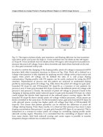
Fig. 1. Cross section of a side-illuminated twin-waveguide pin-photodiode. The equivalent
circuit elements represent physical parameters of the photodiode and parasitic elements.
Electrically, the output of the pin photodiode is fabricated as a coplanar waveguide
transmission line in order to facilitate hybrid integration with the GaAs travelling-wave
amplifier and also for on-wafer high-frequency measurements. Figure 1 indicates how the
parasitic components are connected and how they are related to the physical parameters of
the pin photodiodes.
Photodiodes - World Activities in 2011
6
Here Rs is the p- and n-electrode contact resistance, R j is the resistance representing the
dark current leakage, R p is the resistance of the bulk P+ -InP layer; Cpd is the reverse-bias
junction capacitance, Cd capacitance between p- and n-contact metallization which is
significant at low frequencies, Ls is the inductance of the p/n-contacts to signal/ground
electrodes, Csh and Gsh are the shunt capacitance and conductance of coplanar waveguide
which take into account the electric energy storage inside the transmission line and the
losses caused by the transverse component, Cp is the open circuit at the end of the coplanar
waveguide transmission line, and RL is the load resistance.
In the case of semiconductors photodetectors based on InP materials are the ones most often
used in state of the art long-wavelength optical fiber communication systems. Mixed
compounds such InGaAs(P) and In(Al)GaAs lattice matched to InP are the materials
responsible for detecting long-wavelength light, especially the nondispersion wavelength
(1.3 μm) and loss minimum wavelength (1.55 μm) of silica optical fibers.
The characteristic of these InP based photodetectors are superior to those of conventional
photodiodes composed of elemental Ge, which was the only material applicable for
wavelengths below 1.5 μm . By using a heterostructure, which had not been expected in
group IV elemental semiconductor such as Si and Ge, new concepts and new designs for
high-performance photodetectors have been developed. For example, the absorption region
can be confined to a limited layer, and the InP wide-bandgap layer can serve as a
transparent layer for specific communication wavelength. Recently InGaAs/InP avalanche
photodiodes (ADPs) with a SAM (separation of absorption and multiplication)
configuration have become commercially available.The SAM configuration is thought to be
necessary for high performance APD´s utilizing long wavelenghts.
Because photodiodes operate under reverse-bias, high quality semiconductor layers need to
be produced. To obtain photodiodes that operate at a low bias and have a dark current, it is
necessary to produce epitaxial layers that are pure and that have few effects (such as
dislocations, points defects and impurity precipitates).To get stable and uniform gain in
APDs, in which internal gain is achieved through the carrier avalanche process, the layers in
the avalanche region must be uniform and free of dislocations. Futthermore a planar device
structure requieres that a guardring be used to keep the electric field around the
photoreceptive area from increasing to much.
Fabrication and processing technologies such as impurity diffusion, ion implantation and
passivation will also play important role in the production of reliable photodetectors. The
photodiodes used in received circuits are required to traslate optical signals into electrical
signals faitfully and efficiently.
The reflectance and the internal quantum efficiency are determined the photodiode spectral
responsivity, which is the radiometric characteristic of interest in the fields where these
devices can be used for optical radiation measurements. It presents the experimental set up
for measuring the photodiode reflectance as well as the results of such measurements
related to InGaAs/InP-photodiodes exploited in international laboratories.
The obtained experimental results show that some models of photodiodes have got an anti-
reflecting coating on their sensitive facets and that reflectance does not change with varying
the light polarization state within the measurement uncertain, when the angles of incidence
are less that 7.4 º.
3. Applications of InP photodiodes
Future systems based on microwave and optics such as fiber optic radio communications
will require very high speed InP photodetectors able to work in the microwave or millimeter
An Absolute Radiometer Based on InP Photodiodes
7
wave frequency range. It is well-known that PIN photodetectors limitations are due to
transit time and capacitance.
To increase their cut-off frequency, it is necessary to reduce transit time, so thickness of
absorbing layer, and capacitance. For top-illuminated PIN photodetectors, this will decrease
dramatically the responsivity of the photodetector, and theses detectors are generally used
up to around 20 GHz, as maximum bandwidth. For upper frequencies, the PIN waveguide
photodetector is an attractive device, since it is possible to reduce transit time without
decreasing responsivity, because of the absorbing core waveguide structure. Moreover, the
optical signal is absorbed over a short length (5-10 μm), and the device , so the capacitance,
can be very small. Recently, demonstrations with high responsivity up to 60 GHz at
Thomson LCR1 and even at higher millimeter wave frequencies2 were performed with
device grown on semi-insulating InP substrate. Microwave access is a coplanar line to
reduce parasitics, and the waveguide is a multimode structure to improve the optical
coupling with the optical fiber. Interdigitated Metal Semiconductor Metal (MSM)
photodetectors on AlInAs/GaInAs/InP epilayers were also subject to attention because of
their low capacitance.
Commercially available MSM (New Focus) were developed with 40 GHz cut-off
frequency. Nevertheless, as for PIN photodetectors, high speed MSM photodetectors
require thin absorbing layers together with short electrode spacing, so reduced
responsivity. Solution would be waveguide devices, or MSM coupled with optical
waveguide, but the technology is then more complicated, and the PIN waveguide
photodetector remains the best solution.
PIN photodiode (or MSM photodetector) does not exhibit internal gain. It is the reason
why heterojunction phototransistor (HPT) in the InP/InGaAs material system has been
studied for several years. HPTs could be a good alternative to top illuminated or edge-
coupled PIN photodiodes since they exhibit an internal gain owing to transistor effect,
without high bias voltage as required for avalanche photodiodes and without excess noise
due to avalanching. If we do not consider doping of epilayers, epitaxial structure of HPT
is very similar to the one of PIN waveguide photodiode. It means that waveguide
technique could also be interesting to apply to HPTs for microwave or millimeter wave
applications.
Photodiodes are semiconductor devices responsive to high energy particles and photons.
Photodiodes operate by absorption of photons or charged particles and generate a flow of
current in an external circuit, proportional to the incident power. Planar diffused silicon
photodiodes are P-N junction diodes. A P-N junction can be formed by diffusing either a P-
type impurity, such as Boron, into a N-type bulk or epitaxial silicon wafer, or a N-type
impurity, such as Phosphorus, into a P-type bulk or epitaxial wafer. The diffused area
defines the photodiode active area. To form an ohmic contact, another impurity diffusion
into the backside of the wafer is necessary. The active area is coated with an Anti-Reflection
coating to reduce the reflection of the light for a specific predefined wavelength. The P and
N-sides of the junction have metal pads, which make an electrical contact through dielectric
layers.
Due to the high absorption coefficient, the InGaAs absorption region is typically a few
micrometers thick. The thin absorption layer enables the device to obtain high speed at a
low reverse bias voltage, typically 2-5 volts. The InP window layer is transparent to 1.3μm –
1.55μm wavelengths, thus InGaAs/InP photodiodes do not have slow tail impulse response
associated with the slow diffusion component from the contact layer.
Photodiodes - World Activities in 2011
8
4. Basic photodiode operation
Photodiodes operate under reverse vias to create a depleted region in which photogenerated
electron-hole pairs. In the figure 2 show a schematic cross section of a photodiode ( or
avalanche) with a p(+),(-)n,n(+) structure. It also show the optical absorption, which is
subject to the absorption coefficient of the material for incident light and decreases
exponentially with increasing distance from the diode front p(+).
(a) Cross sectional sketch of p(+), n(-), n(+) diode under reverse bias.
(b) Electric field distribution
(c) Energy band diagram
Fig. 2. Basic operation of a Photodiode.
In the Figure 2(b) and (c) show electric field distribution and the energy band diagram,
respectively. Most photocarriers are designed for use in the fully depleted n-region, so that
they have a high-speed response: Electrons and holes generated within the depletion region
are instantaneously separated by the elelectrical field and drift in the opposite direction,
An Absolute Radiometer Based on InP Photodiodes
9
inducing a photocurrent in the external circuit. On the other hand, minority-carrier holes
excited within an average diffusion length in the undepleted n(+) region adjacent to the
depleted region diffuse into the edge of the depleted junction with some recombination and
are colleted across the high-field region, resulting in a diffusion photocurrent in the external
circuit. Diffusion photocurrent is generally characterized by its slow response to the optical
signal, since the speed of the response depends on the time it takes for the photogenerated
minority carriers to diffuse from where they are generated in the neutral undepleted region
into the edge of the depletion region.
The photodiode should therefore be designed in such a way that there is no optical
absorption in the undepleted neutral region. For the same reason, as well as to reduce the
recombination loss of photocarriers genereted in the P(+) region on the fron side of the
diode, the p(+) region must be as thin as possible.
When the electric field of photodiode is elevated to several hundreds of kilocolts per
centimeter by increasing reverse bias, as internal gain for a primary photocurrent can be
obtained. This gain is a result of the electron-hole pair creation is denominated avalanche
process, initiated by the photogenerated carriers, which creation is in turn governed by the
relation between the strenght of the electric field and the electron and hole impact ionization
rates of the material itself.
4.1 Basic InP PIN photodiodes
In making a simple planar structure the photodiode a double heterostructure consisting of
InGaAs/InP with a inP capping layer is grown, and this growth is followed by selective
impurity diffusion to form the p(+)n(-) junction. A window allowing light to pass through is
formed on the front ( the grown-layer superffice) or back surface of the InP substrate. The
back-illumination type is of a structure often used to obtain the low capacitance desirable for
high-speed operation.
A cross -sectional view of a front-illuminated planar structure InGaAs/InP – PIN
photodiode is show in the figure 3.
Fig. 3. Schematic cross section of a planar structure InP Photodiode.
Photodiodes - World Activities in 2011
10
In the case of InP Photodiodes we need to check something important parameters for
example:
a. Receiver Sensitivity.
b. Response Speed.
c. Dark Current Reduction.
d. High Speed and high quantum efficiency.
e. Reduction of diode capacitance.
f. Large-ionization rate ratio materials for the avalanche layer.
5. InP-photodetectors
At the present time, the InGaAs/InP-photodetectors from different manufactures have
rather low level of noise, a good uniformity of the surface response as well as a wide
dynamic range and linearity.
For these reasons they are exploited in the instruments for measuring optical radiation
within the near infrared (IR) range (800-1600 nm). Furthermore, the InGaAs/InP-
photodetectors are used for maintaining the scale of spectral responsitivity in the same
spectral range in many laboratories. It is presented this chapter devoted to studying the
reflectance of photodiodes from different manufactures.
For this reason, measuring the reflectance of photodiodes is presented in this chapter as a
preliminary step to finding the responsivity. The photodiode response depends on a set of
parameters inherent in the incident light like the spectral distribution, polarization,
modulation of frequency, angle of incidence, and radiant power.
Then, the response is determined by such characteristics of photodetector as the material
refraction index and the structure of diode as well as by some environmental factors, for
example, by the temperature.Photodiodes are semiconductor devices responsive to high
energy particles and photons. Photodiodes operate by absorption of photons or charged
particles and generate a flow of current in an external circuit, proportional to the incident
power. Planar diffused silicon photodiodes are P-N junction diodes. A P-N junction can be
formed by diffusing either a P-type impurity, such as Boron, into a N-type bulk or epitaxial
silicon wafer, or a N-type impurity, such as Phosphorus, into a P-type bulk or epitaxial
wafer. The diffused area defines the photodiode active area. To form an ohmic contact,
another impurity diffusion into the backside of the wafer is necessary. The active area is
coated with an Anti-Reflection coating to reduce the reflection of the light for a specific
predefined wavelength. The P and N-sides of the junction have metal pads, which make an
electrical contact through dielectric layers.
Due to the high absorption coefficient, the InGaAs absorption region is typically a few
micrometers thick. The thin absorption layer enables the device to obtain high speed at a
low reverse bias voltage, typically 2-5 volts. The InP window layer is transparent to 1.3μm –
1.55μm wavelengths, thus InGaAs/InP photodiodes do not have slow tail impulse response
associated with the slow diffusion component from the contact layer.
6. Experimental procedure
To realize our experiments related to measuring the reflectance of InGaAs/InP photodiodes
it have arranged the experimental set-up presented in Figure 4.
An Absolute Radiometer Based on InP Photodiodes
11
Fig. 4. Experimental set-up for measuring the reflectance InGaAs/InP photodiodes
It has exploited an incandescence lamp is the source of white light imaged at the input slit of
the monochromator. This lamp was able to cover the spectral range from 800 to 1600 nm and
had appropriate blocking filters for second – order wavelengths. After the monochromator,
it had placed a linear polarizer and a beam splitter, which serves to monitor temporal
fluctuations of light power. A germanium photodiode was used as the monitoring reference
photodetector.
The experimental set-up included an optical system of mirrors, which consists of two parts.
An upper part (see mirror 7 and germanium photodiode 9) realized monitoring temporal
fluctuations of light power. A bottom part (see mirrors 8, 11; InGaAs/InP-photodiode 10,
and and germanium photodiode 12) formed an image of the monochromator’s exit slit on
Photodiodes - World Activities in 2011
12
the sensitive surfaces of photodiodes. The angle of incidence was equal to 7.4 grades which
was accepted as the normal incidence in this train of measurements. The method of
measurement consists in comparing the response from a germanium photodiode to the
radiation reflected by the InGaAs/InP photodiode with the response from an aluminium
standard mirror whose reflectance is known, so that :
()
()
()
()
p
m
m
I
P
I
λ
λ
ρ
λ
λ
≡
(1)
Here,
()
p
I
λ
is the response to the light reflected by the InGaAs/InP, ()
m
I
λ
is the response
to the light reflected by the mirror, and
()
m
ρ
λ
is the reflectance of a standard mirror. With
this method it has measured the reflectance of photodiodes from different manufacturers.
One part of detectors had a round aperture of 5 mm in diameter and the other part had a
rectangular aperture of 8 x 8 mm.
7. Analysis of reflectance
The grade of light polarization at the output the monochromator was different with varying
the wavelength, figure 5.2 illustrates spectral dependences of the reflectance, which had
been obtained from photodetectors belonging to three different manufacturers. In figures
5.2a and 5.2b that the reflectance of such detectors has a minimum in an area of 1000 – 1600
nm, and they both are related to a structure of layers providing maximal responses in the
spectral interval of mayor utility of these detectors in near IR optics communication. The
first photodiode, see Figure 5a, whose reflectance was minimized, is more efficient that the
second one, see figure 5b.
One can see that this plot presents the other spectrum of reflectance in figure 6, is associated
with a photodiode with rectangular aperture. In this case the reflectance has two minima at
1000 nm and 1600 nm, but the reflectance has a maximum between these minima. This
photodiode is older than previous ones, and it was produced by the other manufacturer.
One can remark that may be it was produced without good enough control, because the
structure of layers on the sensitive surface modifies the reflectance.
The spectrum of reflectance for photodiodes 1 and 4 is presents in figure 7 which belong to
the same manufacturer. The reflectance was measured with linearly polarized and non-
polarized lights, and these pair of measurements gives quite similar results. In fact, the
difference was equal to approximately 2%. The same results are depicted for the
photodiodes 2 and 5, by the second manufacturer. It is important that the results do not
depend on the polarization state of the incident light when the angle of incidence is smaller
10 angular degrees.
All spectrums of reflectance for photodiodes 1-6 is presents in the figure 9, with linearly
polarized and non polarized lights and is possible to see the different behavior of the
photodiodes in the near infrared wavelength.
In fact, in this chapter is studying the behavior of the photodetectors in the near infrared
with the linearly polarized and non polarized lights in the case of the polarized lights the
angle of incidence is smaller 10 angular degrees and is possible observed it doesn’t have
changes in the behavior of the reflectance.
An Absolute Radiometer Based on InP Photodiodes
13
(a)
(b)
Fig. 5. Detector with a round aperture with the diameter of 5 mm
800 1000 1200 1400 1600
0.00
0.05
0.10
0.15
0.20
0.25
Reflectance
Wavelenght (nm)
800 1000 1200 1400 1600
0.06
0.08
0.10
0.12
0.14
0.16
0.18
Reflectance
Wavelenght (nm)
Photodiodes - World Activities in 2011
14
Fig. 6. Detector with a rectangular aperture of 8 x 8mm
Fig. 7. Spectrum of reflectance for photodiodes 1 and 4
800 1000 1200 1400 1600
0.26
0.28
0.30
0.32
0.34
0.36
Reflectance
Wavelenght (nm)
800 1000 1200 1400 1600
0.00
0.05
0.10
0.15
0.20
0.25
Reflectance
Wavelenght (nm)
An Absolute Radiometer Based on InP Photodiodes
15
Fig. 8. Spectrum of reflectance of photodiodes 2 and 5.
Fig. 9. Spectrum of reflectance of photodiodes 1-6.
8001000120014001600
0.06
0.08
0.10
0.12
0.14
0.16
0
.1
8
Reflectance
Wavelenght (nm)
800 1000 1200 1400 1600
0.06
0.08
0.10
0.12
0.14
0.16
0.18
Reflectance
Wavelenght (nm)
800 1000 1200 1400 1600
0.00
0.05
0.10
0.15
0.20
0.25
0.30
0.35
Reflectance
Wavelenght (nm)