Advanced Trends in Wireless Communications Part 15 potx
Bạn đang xem bản rút gọn của tài liệu. Xem và tải ngay bản đầy đủ của tài liệu tại đây (3.35 MB, 35 trang )
Advanced Trends in Wireless Communications
480
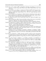
Fig. 25. The 3
rd
order intercept point response of the RF filter
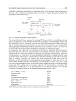
Fig. 26. The related curve of the dynamic range and quality factor
Design of CMOS Integrated Q-enhanced RF Filters
for Multi-Band/Mode Wireless Applications
481
Performance Parameters [11] [12] This work
Technology 0.25μm CMOS 0.5-Si-SOI 0.18μm CMOS
Center frequency 2.14GHz 2.5GHz 2.142GHz
3-dB Bandwidth 60MHz 70MHz 36MHz
Maximum Gain in passband 0dB 14dB 15dB
Noise Figure 19dB 6dB 15dB
Supply voltage
2.5V 3V 1.8V
DC consumption 17.5mW 15mW 15mW
Table 1. The performance comparision of RF active integrated LC filter
Table 1 shows the comparison for published CMOS, and bipolar RF integrated bandpass
filters in the literature. The comparison table demonstrates that the proposed RF filter has
lower power-supply, the highest selectivity, and the largest gain.
5. Conclusion
A 2.14GHz CMOS fully integrated second-order Q-enhanced LC bandpass filter with
tunable center frequency is presented. The filter uses a resonator built with spiral inductors
and inversion-mode MOS capacitors which provide frequency tuning. The simulated results
are shown that the filtering Q and gain can be attained 60 and at 2.14GHz, and the spurious-
free dynamic range (SFDR) is about 56dB with Q=60 and power consumption is about
15mW. The presented filter is suitable for S-band wireless applications.
6. References
[1] B. Georgescu, H. Pekau, J. Haslett and J. Mcrory, Tunable coupled inductor Q-
enhancement for parallel resonant LC tanks, IEEE Trans. Circuit and System-II:
analog and digital signal processing, vol. 50, pp705-713, Oct. 2003.
[2] T.H. Lee, The design of CMOS radio-frequency integrated circuits, U.K.: Cambridge
Univ. Press, pp.390-399, 2004.
[3] W.B.Kuhn, F. W. Stephenson, and A. Elshabini-Riad, A 200MHz CMOS Q-enhanced LC
bandpass filter, IEEE J. Solid-State Circuits, vol. 31, pp.1112-1122, Oct. 1996.
[4] W. B. Kuhn, D. Nobbe, D. Kelly, A. W. Orsborn, Dynamic range performance of on-chip
RF bandpass filters, IEEE Trans. Circuit and Systems-II:analog and digital signal
processing, vol. 50, pp. 685-694, Oct. 2003.
[5] S. Bantas, Y. Koutsoyannopoulos, CMOS active-LC bandpass filters with coupled
inductor Q-enhancement and center frequency tuning, IEEE Trans. Circuits and
Systems-II: express briefs, vol. 51, pp.69-77 Feb. 2004.
[6] S.Pipilos, Y.P. Tsividis, J. Fenk, and Y. Papanaos, A Si 1.8 GHz RLC filter with tunable
center frequency and quality factor, IEEE J. Solid-State Circuits, vol. 31, pp. 1517-
1525, Oct. 1996.
[7] F. Dulger E. S. Sinencio and J. Silva-Martinez, A 1.3V 5mW fully integrated tunable
bandpass filter at 2.1GHz in 0.35um CMOS, IEEE J. Solid-State Circuits, vol. 38 pp.
918-927, June 2003.
Advanced Trends in Wireless Communications
482
[8] W.B. Kuhn, A. Elshabini-Riad, and F. W. Stephenson, Center-tapped spiral inductors for
monolithic bandpass filters, Electron. Lett., vol. 31, pp.625-626, Apr. 1995.
[9] F. Krummenacher, G. V. Ruymbeke, Integrated selectivity for narrow-band FM IF
systems, IEEE J. Solid-State Circuits, vol. SC-25, pp.757-760, June 1990.
[10] T. Soorapanth, S. S. Wong, A 0dB IL 2140 ± 30 MHz bandpass filter utilizing Q-
enhanced spiral inductors in standard CMOS, IEEE J. Solid-State Circuits vol.37, pp.
579-586, may, 2002.
Section III: A fully integrated CMOS active bandpass filter for multi-band RF
front-ends
1. Introduction
Now, the fast-growing market in wireless communications has led to the development of
multi-standard mobile -terminals [1-3]. This creates a strong interest toward the highly
integrated RF transceivers in a compact and low-cost way. So, it is becoming more and more
attractive to have a single chip of the complete CMOS multi-band transceiver in the
industrial, scientific, and medical (ISM) bands. However, the integrated high-performance
filters working at RF frequency still remain the one of the most difficult parts in the
integrated RF front-ends. The existence of large interference, spurious tones, unwanted
image and carrier frequencies, as well as their harmonics in the wireless communication
environment demands the use of RF filters with high selectivity in the RF front-ends as
shown in Figure 27.
Fig. 27. Multi-Band RF front-end designs
In fact, in current gigahertz-range transceivers, the bulky and expensive off-chip bandpass
filters [2] are still required to handle the existence of large out-of-band interference as shown
in Figure 1(a). Furthermore, it increases the size, power consumption, and cost of multi-
standard transceivers significantly by adding different copies of discrete filters for different
bands. Great efforts have been made to use an on-chip tunable Q-enhanced filter to replace
such off-chip preselect filter.
To this extent, recent researches on integrated filter design have fallen into the active-LC
category [5]-[11]. Filters of this category are built around on–chip spiral inductors and
capacitors used as LC resonant tanks, whereas an important cause for the limited integration
of RF filters is the low quality factor of monolithic spiral inductors. These inductors are
inherently lossy due to ohmic losses in the metal traces and due to substrate resistance and
eddy currents. This problem has been addressed by using various methods such as
patterned ground shields and geometry improvements, but the Q factor of integrated
inductors is still generally limited to a value less than 20 [12] in standard RF CMOS process.
Design of CMOS Integrated Q-enhanced RF Filters
for Multi-Band/Mode Wireless Applications
483
For multi-band RF front-end designs, a suitable on-chip tunable filter is available, but the
tunable nature of the on-chip passive inductors is hard.
Compared with the passive inductors, the RF bandpass filter using active inductors can not
only achieve wide frequency tuning range and high quality factor, but also occupy the small
chip areas. However, it also pays for the higher noise and the worse linearity. In commercial
designs as shown in Fig. 1 (a), an LNA combined with a 3dB insertion loss discrete filter
typically achieves a net 5dB noise figure, 17dB gain, and 1dB input compression point about
-17dBm if the input P1dB of LNA is about -20dBm, while consuming 15mW [4]. If the filter
using active inductors is located in the RF front-end as shown in Fig. 1(b), and the input
P1dB of LNA is about 20dBm, the proposed RF filter and the LNA can achieve a net less
than 4dB, and a net more than or equal to -20dBm input compression point with 15dB gain,
so the proposed RF filter combined with other RF modules will satisfy the performance of
the moderate noise figure and linearity of RF system requirements such as Bluetooth,
802.11b and so on.
The section is organized as follows. Section 2 presents the novel Q-enhanced active inductor
topology, as well as the analysis of the noise figure linearity and stability. Section 3
describes the RF bandpass filter based on the active inductors and the measured results of
the filter are demonstrated. Finally, conclusion is given in section 4.
2. Circuit principle
2.1 Proposed active inductor
An often–used way for making active inductors is through the combination of a gyrator and
capacitor, but designing high-Q active inductors at GHz with opamps or standard
transconductance-C techniques is very difficult due to relatively significant power
consumption and noise. The active inductor based on the principle of gyration, consisting of
minimum-count transistors can be operated at GHz easily because f
T
of single transistor is so
high as hundreds of GHz. A class of active inductors have been proposed by researchers
[14][19][20] in Figure 27. A common feature of these active inductor topologies is that they
all employ some kind of shunt feedback to emulate the inductive impedance in Figure 28.
Fig. 28. The proposed CMOS active inductor topology
Advanced Trends in Wireless Communications
484
Intuitively, the circuits can be explained as follows: the input signal at the source of M2 will
generate a current g
m2
V
i
at the drain of M2, this current will be integrated on the gate-source
capacitance C
gs1
. The voltage at the gate of M1 will then generate the input current, thus
generating the inductive loading effect. Compared with the active inductor proposed in
Figure 28(a) and improved (b) or (c), we found the active inductor in Fig. 28(a) has some
advantages over the active inductor in Figure 28(b) or (c). As can be seen from the circuit
figure, the minimum voltage for the active inductor itself is only max(V
gs1
+V
ds1
+V
in
,
V
gs2
+V
ds2+
V
gs1
+V
in
). Therefore, the circuit in Fig 28(a) is better than the circuit in (b) or (c),
and it has two transistors contributing noise directly to the input. In our design, the current-
reused active inductor based on (a) is chosen.
Fig. 29. The small-signal equivalent circuit of the proposed active inductor
A conceptual illustration of the proposed active inductor is shown in Figure 27. A more
detailed small- signal representation of Figure 28(a) is shown in Figure 29, where g
O
is the
drain-source conductance and g
OC
represents the loading effect of the nonideal biasing
current source Z
load
. The impedance of Z
in
can be expressed as
≡=
in
in
pp
L
in
V
ZR//C//Z
I
(2.24)
where the inductive impedance of Z
in
is
1 221
12 2 1 2 1 2 2
+
+++
=
+−++ + +
oc o gs gd gd
L
mm m m oc gs gd o gd
ggs(C C C)
Z
g g [ g g g s(C C )]( g sC )
(2.25)
The small-signal analysis of the circuit in Figure 28(a) shows that Z
in
is a parallel RLC
resonant tank with the following values:
1
21
11
1
=≈
m
om
Rp ||
g
gg
1
=
pg
s
CC
2
12
≈
gs
p
mm
C
L
gg
1
12
+
≈
oc o
L
mm
gg
r
gg
(2.26)
where r
L
is the intrinsic resistor of the active inductor. The self-resonant frequency ω
0
and
intrinsic quality-factor of the inductor is
12
012
12
ω
≈=ωω
mm
tt
gs gs
gg
CC
(2.27)
Design of CMOS Integrated Q-enhanced RF Filters
for Multi-Band/Mode Wireless Applications
485
and
21
0
012
=≈
ω
p
m
g
s
p
m
g
s
Rgc
Q
Lgc
(2.28)
where ω
t1
and ω
t2
are the unity-gain frequency of M1 and M2, respectively.
2.2 Noise analysis
Unlike the passive inductor where the damping resistor rL is the main noise contributor, the
noise in active inductor originates from the thermal noise of MOS transistor channel [14],
[15]. By referring to the transistor noise sources to the terminals of the active inductor in
Figure 28(a), the noise figure of the circuit will be computed considering, for simplicity, only
three main noise sources, i.e., the thermal noise of the two transistors (M1 and M2) and the
noise of the load impedance Rp (i.e.
1
load
O
||Z
g
). where
2
11
4=γΔ
nm
vkTf/g, and
2
22
4=γΔ
nm
ikTfg, kT is Boltzmann’s constant times temperature in Kelvin, and γ is chosen
empirically to match the observed thermal noise behavior of a given fabrication process.
Computing the transfer functions from all noise sources to the output node, the following
expression for the NF (at the resonance frequency) can be obtained
2
1
2
2
11
1
1
+
γ
=+ +γ +
⋅
mS
mS
mS mS P
(
g
R)
NF g R
g
R
g
RR
(2.29)
Where R
S
is the source impedance. The second term in the right-hand side of (6) represents
the noise contributed by transistor M1 and it has the same expression as for a common-gate
amplifier. However, in this case, due to the feedback in the gyrator, g
m1
can be made larger
than 1/R
S
while still ensuring matching conditions. The third term represents the noise
introduced by the feedback transistor M2. Consistently with the intuition, transistor M2
injects noise directly at the input, and its transconductance has to be small to have a low
noise. The fourth term in the equation represents the noise contributed by the load. If
g
m1
R
S
>>1, this term becomes approximately equal to R
S
/R
P
. Notice that increasing R
P
(i.e.,
increasing the quality factor of the resonant load) reduces the noise contributed by the load
but also the noise of M2, since it results in a reduction of g
m2
.
2.3 Nonlinear distortion
As shown in Fig. 27, the distortion is mainly influenced by two factors: the additional current
path provided by M2 and the effect of negative feedback on both the gate-source voltage
swing across M1 and its DC bias point. The analytical expression for the circuit input P1dB
can be found from Sansen’s theory [13]. Considering the transistor in strong inversion, the
input P1dB for the circuit as a function of the transconductance of transistors becomes
2
2
112
12
0 244
21
12
=⋅+
−
in
in, dB m m S p
mm Sp
.V
V(
gg
RR)
ggRR
(2.30)
Where V
in
is the input voltage, and the loop gain of the circuit is given by g
m1
g
m2
R
S
R
p
.
According to (2.30), the distortion of the circuit can cancel completely for specific values of
Advanced Trends in Wireless Communications
486
the loop gain. This causes the large difficulty to maintain over a wide range of transistor
variables.
2.4 Q-enhanced technique and stability analysis
Since the basic concept in the Q-enhanced LC filter is to use lossy LC tank, it is necessary to
implement a loss compensation to boost the filter quality factor incorporating negative-
conductance. Negative conductance g
mF
realizes the required negative resistance to
compensate for the loss in the tank. The effective quality factor [6] of the filter at the
resonant frequency can be shown to be
0
1
=
−
en
mF
p
Q
Q
g
R
(2.31)
Where Q
0
is the base quality factor of the LC tank, which is dominated by the equivalent
inductor. Theoretically it can be set as high as desired with appropriate g
mF
. Indeed, the
filter core can be tuned to oscillate if negative transconductance is sufficiently large, i.e.,
greater than 1/R
P
.
Additionally, the main problem is that the use of shunt feedback by M2 to compensate the
loss resistance of the active inductor can result in potential instability depending on the filter
terminating impedances yet. In order to make sure that the circuit is stable, the poles of the
circuit must be in the left half-plane [16], [17]. In this condition, according to (1), using
closed-loop analysis, the circuit will be stable provided that
212
12
2
+
<++
gs gd o
mmoc
gd
(C C )g
ggg
C
(2.32)
Simultaneously it must be ensured that the magnitude of the input reflection coefficient is
less than unity i.e.
11
1
<
S . Due to the stability problem, we should determine the reasonable
transconductance g
m1
and g
m2
in order that the trade-offs between noise, Q enhancement
and stability will satisfy the requirements of the communication systems.
3. Design of the RF filter and its measured results
3.1 Circuit design
The complete prototype circuit of the proposed second-order RF bandpass filter based on
the active inductor topology is shown in Figure 30. This circuit consists of three different
stages, including two differential high Q-enhancement active inductors, negative impedance
and buffers. Common-drain transistors M11, M13 and M12, M14 are employed for the
output buffer stages. This common drain configuration can offer to minimize the loading
effect and output impedance matching.
M1, M3, M5 and M2, M4, M6 construct LC-resonant circuit which is made up of the active
inductor respectively. Note that the transistor M5 and M6 are respectively used to amplify
the signal of shunt feedback in the active inductor topology in order to boost the impedance
of active inductors. M7, M8 and M9, M10 consisting of unbalanced cross-coupled pairs are
employed not only to produce negative resistance for canceling the inductor loss, but also
increase linearity of the filter when the signal is large. The transistors and capacitors are
sized to optimize gain in the passband, noise figure, and linearity. Transistors M1, M2 have
a length/width ratio of 2um/0.18um, M3, M4 have 4um/0.18um, M5, M6 have
Design of CMOS Integrated Q-enhanced RF Filters
for Multi-Band/Mode Wireless Applications
487
20um/0.18um, and M7, M8 have 0.4um/0.2um and M9, M10 have 0.3um/0.18um. For the
output buffers, transistors M11, M12 have a length/width ratio of 3um/0.18um, and M13,
M14 have 2um/0.18um. The input capacitance is about 120ff. The DC bias current I
Q1
and
I
Q2
can be used to tune the Q of the active inductors and the transconductance of the cross-
coupled pairs. V
b
and V
c
are bias voltages which are used for DC operating state of the filter.
The DC bias currents I
bia1
and/or I
bia2
can be adjusted to tune the center frequency of the
circuit and also change the Q of the inductance in Fig. 3.
Fig. 30. The fully Q-enhancement bandpass filter
3.2 Measured results
The circuit is fabricated in 0.18-um UMC-HJTC CMOS process through the educational
service. The die photograph of the fabricated circuit is shown in Figure 31. To ensure the
fully differential operation, a symmetrical layout is used for the design. The total chip area is
0.7×0.75mm
2
including the pads, where the active area occupies only 0.15×0.2mm
2
.
Fig. 31. Photomicrograph of the Q-enhanced RF bandpass filter
Advanced Trends in Wireless Communications
488
The two-port S-parameter measurements were made with the vector network analyzer
Agilent E8363B. Noise measurements were made with a spectrum analyzer equipped with
power measurement software and a noise source. The 1-dB compression point
measurements were made with a spectrum analyzer and a power meter. The measured RF
bandpass filter forward transmission response, S21, is shown in Figure 32, Figure 33 and
Figure 34, respectively. Figure 32 shows the passband center frequency is 1.92GHz and 3-dB
bandwidth is about 28MHz. The maximum gain in the passband is about 11.64dB and the
input return loss, S11 is -14.67dB in Figure 32. In Figure 33, the center frequency is about
2.44GHz and 3-dB bandwidth is about 60MHz. The maximum gain in the passband is about
5.99dB. Moreover, the S21 at about center frequency 3.82GHz is about 12dB and return loss
S11 is about -29dB as shown in Figure 34.
Fig. 32. Measured bandpass filter insertion loss S21 and return loss S11 at center frequency
about 1.92GHz
Fig. 33. Measured bandpass filter insertion loss S21 and return loss S11 at center frequency
about 2.44GHz
Design of CMOS Integrated Q-enhanced RF Filters
for Multi-Band/Mode Wireless Applications
489
Fig. 34. Measured bandpass filter insertion loss S21 and return loss S11 at the center
frequency about 3.82GHz
Fig. 35. P1dB measurement at center frequency about 2.44GHz
A measurement to the input 1dB compression point of the circuit can be obtained by
sweeping the input power to the tank and measuring the output power. As the input power
is increased, the input impedance presented by the Q-enhanced active inductor tanks begins
to drop due to nonlinear effects, which can be observed when the output power no longer
depends on the input power in a linear fashion as shown in Figure 35. The measured
bandpass filter P1dB input power compression point is -15dBm at the center frequency
about 2.44GHz passband. The noise figure of 18dB was also measured by disconnecting the
input signal. The RF filter has wide-tuning range from the center frequency about 1.92GHz
to 3.82GHz when the DC voltage sources of the controlled bias currents Ibia1 and/or Ibia2
are adjusted from 0.5 to 1.5V or vice versa. The noise figure evaluated in each band gives the
Advanced Trends in Wireless Communications
490
following results: 15dB for center frequency 1.92GHz, 18dB for center frequency about
2.44GHz, 20dB for center frequency about 3.82GHz. Furthermore, 1-dB compress point is
about -17dBm, -15dBm, -18dBm respectively.
Ref. [8] [9] [10] [11] This work
Process
0.25um-
CMOS
0.5-Si-SOI
0.18um-
CMOS
0.18um-
CMOS
0.18um-
CMOS
Die area
3.5mm
2
2.5mm
2
2.25mm
2
0.81mm
2
0.53mm
2
N-orders
6 2 3 4 2
f
center
2.14GHz 2.5GHz 2.36GHz 2.03GHz 2.44GHz
-3dB Bandwidth
60MHz 70MHz 60MHz 130MHz 60MHz
Tuning range
- 250MHz - 60.9MHz 1900MHz
Noise figure
19dB 6dB 18 dB 15 dB 18 dB
Mid-band gain
0dB 14dB -1.8dB 0dB 6dB
Supply voltage
2.5V 3V 1.8V 1.8V 1.8V
FOM
72 82 78 77 81
Table 2. Comparison of the RF bandpass filters Performance
The summary of the measured performance and the comparisons of the performance among
the fabricated RF filters in CMOS and other process is given in Table 2. A figure of merit [18]
(FOM) which allows comparison between other RF filters in silicon is given as
1
⋅
⋅⋅
=
⋅
dBW center
f
ilter
DC
NP f Q
FOM
PNF
(2.33)
where N is the number of poles, P
1dBW
is the inband 1-dB compression point in Watt, f
center
is
the center frequency, Q
filter
is the ratio of the center frequency and the 3-dB bandwidth, P
DC
is the DC power dissipation in Watt, and NF is the noise figure (not in dB). It has shown
from Table II that the filter presented in this work achieves a good FOM with higher quality
factor and gain in the passband, and the tuning range is the largest, and the chip area is the
smallest.
4. Conclusion
The design and implementation of tunable RF bandpass filter in 0.18um CMOS process have
been introduced and verified, which demonstrate that the RF bandpass filter can achieve
Design of CMOS Integrated Q-enhanced RF Filters
for Multi-Band/Mode Wireless Applications
491
high quality factor and large tuning range from 1.92GHz to 3.82GHz. Although the noise
and linearity of the proposed active inductors are inferior to passive ones, the smallest chip
area, and the largest tenability make them apply to the multi-band on-chip wireless systems
in future.
5. References
[1] A. Tasic, W.A. Serdijn, J.R. Long. Adaptive multi-standard circuits and systems for
wireless communications. IEEE Magazine On Circuits and Systems, vol. 6, no. 1, pp.
29-37, Quarter, 2006.
[2] Y. Satoh, O. Ikata, T. Miyashita, and H. Ohmori, RF SAW filters Chiba Univ., Japan, 2001
[Online]. Available:
/Symp2001/PAPER/SATOH.PDF.
[3] A. Tasic, S. Lim, W.A. Serdijn, J.R. Long. Design of adaptive multi- mode RF front-end
circuits. IEEE J. of Solid-State Circuits, vol. 42, pp. 313-322, Feb. 2007.
[4] MBC13916 General purpose SiGe: C RF Cascade Amplifier. Motorola, Data Sheet.
[5] S. Li, N. Stanic, Y. Tsividis. A VCF loss-control tuning loop for Q- enhanced LC filters.
IEEE Trans. On Circuits and Systems-II: express briefs, vol. 53, pp. 906-910, Sep. 2006.
[6] W. B. Kuhn, D. Nobe, N. Kely, A.W. Orsborn. Dynamic range performance of on-chip RF
bandpass filters. IEEE Trans. On Microwave Theory and Techniques, vol. 50, pp. 685-
694, Oct. 2003.
[7] B. Bantas,Y. Koutsoyannopoulos. CMOS active-LC bandpass filters with coupled-
inductor Q-enhancement and center frequency tuning. IEEE Trans. Circuits and
Systems-II: express briefs, vol. 51, pp. 69-76, Feb. 2004.
[8] T. Soorapanth S. S. Wong. A 0-dB IL, 2140±30MHz bandpass filter utilizing Q-enhanced
spiral inductors in standard CMOS. IEEE J. of Solid-State Circuits, vol. 37, 579-586,
May 2002.
[9] X. He, W. B. Kuhn. A 2.5GHz low-power, high dynamic range, self-tuned Q-enhanced
LC filter in SOI. IEEE J. of Solid-State Circuits, vol. 40, pp.1618-1628, Aug. 2005.
[10] J. Kulyk, J. Haslett. A monolithic CMOS 2368±30MHz transformer based Q-enhanced
series-C coupled resonator bandpass filter. IEEE J. of Solid-State Circuits, vol. 41,
362-374, Feb. 2006.
[11] B. Georgescu, I. G. Finvers, F. Ghannouchi. 2 GHz Q-enhanced active filter with low
passband distortion and high dynamic range. IEEE J. of Solid-State Circuits, vol. 41,
pp.2029-2039, Sep. 2006.
[12] Y.Cao, R. A. Groves, X. Huang et. al. Frequency-independent equivalent-circuit model
for on-chip spiral inductors. IEEE J. of Solid-State Circuits, vol. 38, 419-426, Mar.
2003.
[13] W. Sansen. Distortion in elementary transistor circuits. IEEE Trans. On Circuits and
Systems-II: express briefs, vol. 46, 315-325, Mar. 1999.
[14] Z. Gao, M. Yu, Y. Ye, and J. Ma. A CMOS RF tuning wide-band bandpass filter for
wireless applications. In Proc. IEEE Int’l Conf. SOC, pages 79–80, Spet. 2005.
[15] G. Groenewold. Noise and group delay in active filters. IEEE Trans. On Circuits and
Systems-I: regular papers, vol. 54, pp. 1471-1480, July, 2007.
[16] P. R. Gray and R. G. Meyer, Analysis and Design of Analog Integrated Circuits, 3rd ed.
New York: Wiley, 1993.
Advanced Trends in Wireless Communications
492
[17] Robert W. Jackson. Rollett Proviso in the stability of linear Microwave circuits-A
tutorial. IEEE Trans. on Microwave Theory and Techniques, vol. 54, pp. 993-1000, Mar.
2006.
[18] K.T. Christensen, T. H. Lee, E. Bruun. A high dynamic range programm- able CMOS
Front-end filter with tuning range from 1850-2400 MHz. Norwell, MA: Kluwer,
2005.
[19] A.Karsilayan and R. Schaumann A High-Frequency High-Q CMOS Active Inductor
with DC Bias Control, Proc. IEEE Midwest Symp. Circ. Syst. (MWSCAS), Aug. 2000.
[20] Y. Wu, M. Ismail, and H. Olsson, A novel fully differential inductorless RF bandpass
filter in Proc. IEEE Int. Symp. Circuit and System (ISCAS), Geneva, Switzerland, May
2000, pp. 149-152.
25
High-frequency Millimeter Wave Absorber
Composed of a New Series of
Iron Oxide Nanomagnets
Asuka Namai and Shin-ichi Ohkoshi
Department of Chemistry, School of Science, the University of Tokyo,
Japan
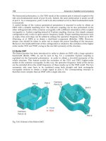
1. Introduction
High-speed wireless communications using millimeter waves (30–300 GHz) have received
much attention as a next-generation communication system capable of transmitting vast
quantities of data such as high-definition video images. Due to the recent development of
transistors composed of complementary metal-oxide semiconductors or double
heterojunction bipolar transistors,
1-5
electromagnetic (EM) waves in the millimeter wave
range are beginning to be used in high-speed wireless communication.
6-8
Especially, for 60
GHz-band wireless communication, Wigig alliance was established in December 2009, and
televisions and local area network (LAN) using 60 GHz millimeter wave have been
extensively researched and developed. Millimeter wave wireless communication is
anticipated to realize a transmission rate that is several handred times greater than current
wireless communication. On the other hand, in a wireless communication, electromagnetic
interference (EMI) is a problem. In addition, the unnecessary EM waves should be
eliminated to protect the human body, although the potential health effects due to the
millimeter wave have not yet been understood.
9
To solve these problems, millimeter wave
absorbers need to be equipped with electronic devices such as isolators or be painted on a
wall of building, etc. However, currently materials that effectively restrain EMI in the region
of millimeter waves almost do not exist. Thus, finding a suitable material has received much
attention. Insulating magnetic materials absorb EM waves owing to natural resonance.
Particularly, a magnetic material with a large coercive field (H
c
) is expected to show a high-
frequency resonance. In recent years, we firstly succeeded to obtain a single phase of ε-Fe
2
O
3
nanomagnet (Figure 1), and found that ε-Fe
2
O
3
nanomagnet exhibited an extremely large H
c
value of 20 kOe at room temperature, which is the highest H
c
value for insulating magnetic
materials.
10-19
In this paper, we report a new millimeter wave absorber composed of ε-
Ga
x
Fe
2-x
O
3
(0.10 ≤ x ≤ 0.67) nanomagnets, which shows a natural resonance in the range of
35–147 GHz at room temperature.
20
This is the first example of a magnetic material which
shows a natural resonance above 80 GHz. In addition, the study of the magnetic
permeability of ε-Ga
x
Fe
2-x
O
3
was performed in 60 GHz region (V-band). By analyzing
electromagnetic wave absorption properties, the magnetic permeability (μ’-jμ”) and
dielectric constant (ε’-jε”) of ε-Ga
x
Fe
2-x
O
3
were evaluated.
21
Advanced Trends in Wireless Communications
494
(a) (b)
25 nm
a-axis
c
b
a
Fig. 1. (a) TEM image of ε-Fe
2
O
3
at high magnification. The inset is the high resolution
image. (b) Crystal structure of ε-Fe
2
O
3
.
2. Synthesis, crystal structures and magnetic properties
In this section, we show the synthesis, crystal structures and magnetic properties of a new
millimeter-wave absorber composed of ε-Ga
x
Fe
2-x
O
3
(0.10 ≤ x ≤ 0.67) nanoparticles.
2.1 Synthesis of ε-Ga
x
Fe
2-x
O
3
nanomagnets
A new series of ε-Ga
x
Fe
2-x
O
3
(0.10 ≤ x ≤ 0.67) nanoparticles was synthesized by the
combination of reverse micelle and sol–gel techniques or only the sol–gel method. Figure 2
describes the flowchart of the synthetic procedure for ε-Ga
x
Fe
2-x
O
3
nanoparticles. In the
combination method between the reverse-micelle and sol-gel techniques, microemulsion
systems were formed by cetyl trimethyl ammonium bromide (CTAB) and 1-butanol in n-
octane. The microemulsion containing an aqueous solution of Fe(NO
3
)
3
and Ga(NO
3
)
3
was
mixed with another microemulsion containing NH
3
aqueous solution while rapidly stirring.
Then tetraethoxysilane was added into the solution. This mixture was stirred for 20 hours
and the materials were subsequently sintered at 1100 °C for 4 hours in air. The SiO
2
matrices
were etched by a NaOH solution for 24 hours at 60 °C.
2.2 Morphology and crystal structure
In the transmission electron microscope (TEM) image, sphere-type particles with an average
particle size between 20-40 nm are observed as shown in the inset of Figure 2. Rietveld
analyses of X-ray diffraction (XRD) patterns indicate that materials of this series have an
orthorhombic crystal structure in the Pna2
1
space group (Figure 3). This crystal structure has
four nonequivalent Fe sites (A-D), i.e., the coordination geometries of the A-C sites are
octahedral [FeO
6
] and that of the D site is tetrahedral [FeO
4
]. For example, in the case of x=
0.61, 92% of the D sites and 20% of the C sites are substituted by Ga
3+
ions, but the A and B
sites are not substituted because Ga
3+
(0.620 Å), which has a smaller ionic radius than Fe
3+
(0.645 Å),
22
prefers the tetrahedral sites.
The shade of blue in Figure 3 depicts the degree of
Ga substitution.
High-frequency Millimeter Wave Absorber Composed of a New Series of Iron Oxide Nanomagnets
495
Fig. 2. Schematic illustration of the synthetic procedure of ε-Ga
x
Fe
2-x
O
3
nanocrystal using
combination method between reverse-micelle and sol-gel techniques. The inset is TEM
image of ε-Ga
x
Fe
2-x
O
3
particles.
Ga
3+
occupancy
0%
100%
A
C
D
B
ε-Ga
0.15
Fe
1.85
O
3
ε-Ga
0.47
Fe
1.53
O
3
ε-Ga
0.67
Fe
1.33
O
3
Fig. 3. Crystal structure of ε-Ga
x
Fe
2-x
O
3
. Degrees of Ga substitution at each Fe site (A–D)
described by the shade of blue.
2.3 Magnetic properties
The magnetic properties of this series are listed in Table 1. The field-cooled magnetization
curves in an external magnetic field of 10 Oe show that the T
C
value monotonously
decreases from 492 K (x= 0.10) to 324 K (x= 0.67) as x increases (Figure 4a). Figure 4b shows
the magnetization vs. external magnetic field plots at 300 K. The H
c
value decreases from
15.9 kOe (x= 0.10) to 2.1 kOe (x= 0.67). The saturation magnetization (M
s
) value at 90 kOe
increases from 14.9 emu g
−1
(x= 0.10) to 30.1
(x= 0.40) and then decreases to 17.0 (x= 0.67).
Advanced Trends in Wireless Communications
496
x= 0.10 x= 0.22 x= 0.29 x= 0.35 x= 0.40 x= 0.47 x= 0.54 x= 0.61 x= 0.67
T
C
(K) 492 470 453 441 432 407 385 355 324
M
s
(emu/g) 300 K 14.9 24.7 27.4 28.7 30.1 28.5 25.4 23.3 17.0
2 K 19.2 36.1 42.1 47.5 52.0 52.7 51.0 51.6 42.8
H
c
(kOe) 300 K 15.9 11.6 10.0 9.3 8.8 6.8 5.5 4.7 2.1
2 K 15.5 15.7 14.1 13.7 13.4 12.8 13.1 13.7 14.2
Table 1. Magnetic properties of
ε
-Ga
x
Fe
2-x
O
3
.
-30
-20
-10
0
10
20
30
M / emu g
-1
-40 -20 0 20 40
H / kOe
(a) (b)
7.0
6.0
5.0
4.0
3.0
2.0
1.0
0.0
M / emu g
-1
5004003002001000
T / K
600
400
200
0
T
C
/ K
0.80.40
x
30
20
10
0
M
s
/emu g
-1
0.80.40
x
Fig. 4. Magnetic properties of ε-Ga
x
Fe
2-x
O
3
. (a) FCM curves for x= 0.10 (black), 0.22 (red), 0.40
(green), 0.54 (light blue), and 0.67 (magenta) in the external magnetic field of 10 Oe. (b)
Magnetization vs. external field plots for x= 0.10 (black), 0.22 (red), 0.40 (green), 0.54 (light
blue), and 0.67 (magenta).
The changes in magnetic properties were understood by the replacement of magnetic Fe
3+
(S= 5/2) by non-magnetic Ga
3+
(3d
10
, S= 0). ε-Fe
2
O
3
is a collinear ferrimagnet at room
temperature where the magnetic moments at the B and C sites (M
B
and M
C
sublattice
magnetization) are antiparallel to the A and D sites (M
A
and M
D
sublattice magnetization),
i.e., M
total
= M
B
+ M
C
– M
A
– M
D
.
15,23
In addition, M
D
sublattice magnetization is smaller than
the other three sublattice magnetization. Ga
3+
substitution reduces the M
D
sublattice
magnetization value due to selective substitution at the D sites in the region of 0.10 ≤ x ≤
0.40. Hence, M
total
values of ε-Ga
x
Fe
2-x
O
3
system increase as the x values increase. On the
other hand, the decrease of M
total
at 0.47 ≤ x is caused by Ga replacement at the C, B, and A
sites.
3. Millimeter wave absorption of ε-Ga
x
Fe
2-x
O
3
nanomagnets
In this section, we deal with the millimeter wave absorption due to the natural resonance in
ε-Ga
x
Fe
2-x
O
3
nanoparticles.
3.1 Natural resonance
In general, when an EM wave is irradiated into a ferromagnet, the gyromagnetic effect leads
to resonance, which is called a “natural resonance” (Figure 5a). In a ferromagnetic material
High-frequency Millimeter Wave Absorber Composed of a New Series of Iron Oxide Nanomagnets
497
with a magnetic anisotropy, the direction of magnetization is restricted around the magnetic
easy-axis. Once an external magnetic field tilts the magnetization, then the magnetization
starts to precesses around the easy-axis due to the gyromagnetic effect. When this
precession of magnetization resonates with an applied EM wave, a natural resonance occurs
and EM wave absorption is observed.
24
The natural resonance frequency (f
r
) is proportional
to the magnetocrystalline anisotropy (H
a
), which is expressed by f
r
= (ν/2π)H
a
, where ν is the
gyromagnetic ratio. Common magnetic materials such as spinel ferrite show EM wave
absorption in a few GHz region, and even a f
r
value of metal-substituted barium ferrite is 80
GHz or less.
EM wave
M
H
a
N
S
large
H
ex
M
H
c
small
Abs.
f
r
highlow
Signal
generator
analyzer
Port 1 Port 2
S
21
S
11
sample
A
ntenna
(a)
(b)
Fig. 5. (a) Schematic illustration of the natural resonance due to the gyromagnetic effect.
Precession of magnetization (M) around an anisotropy field (H
a
) causes electromagnetic
wave absorption. Resonance frequency (f
r
) is expressed as f
r
= (ν/ 2π) H
a
. In magnets of a
uniaxial magnetic anisotropy, f
r
is proportional to magnetic coercive field (H
c
). (b) Diagram
of the free space millimeter wave absorption measurement system.
3.2 Millimeter wave absorption properties
The EM absorption properties (V-band; 50-75 GHz, and W-band; 75–110 GHz) were
measured at room temperature using a free space EM wave absorption measurement system
(Figure 5b). The powder-form samples were filled in a 30 mm
φ
× 10 mm quartz cell with the
fill ratios of ca. 40%. The reflection coefficient (S
11
) and permeability coefficient (S
21
) were
Advanced Trends in Wireless Communications
498
obtained, and the absorption of the EM waves was calculated by the following equation:
(Absorption) = -10log[|S
21
|
2
/(1-|S
11
|
2
)] (dB). An absorption of 20 dB indicates that 99% of
the introduced EM waves are absorbed, which is the target value for EM absorbers from an
industrial point of view.
The center of Figure 6 shows millimeter wave absorption spectra of the samples between x=
0.61 and 0.29 in the frequency region of 50–110 GHz. The sample for x= 0.61 shows a strong
absorption at 54 GHz. As x decreases, the frequency of the absorption peak shifts to a higher
one, i.e., 64 GHz (x= 0.54), 73 GHz (x= 0.47), 84 GHz (x= 0.40), 88 GHz (x= 0.35), and 97 GHz
(x= 0.29). In the case of samples for x= 0.67, 0.22, 0.15 and 0.10, the absorption peaks exceed
the measurement range (50–110 GHz). To confirm the frequency of these materials, hand-
made apparatuses for the range of 27–40 GHz and 105–142 GHz were prepared. As a result,
the sample for x= 0.67 showed the absorption peak at 35 GHz (Figure 6, left). In the
frequency range of 105–142 GHz, the peak frequencies for x= 0.22 and 0.15 are observed at
115 and 126 GHz, respectively, and that for x= 0.10 is estimated to be observed at 147 GHz
by supplementation of the spectrum using the Lorentzian function (Figure 6, right). The
absorption intensities of this series are strong (for example, the absorption intensity for x=
0.40 reaches 57 dB (99.9998%)).
As mentioned above, the f
r
value is proportional to the magnetocrystalline anisotropy field
(H
a
), which is expressed by f
r
= (ν/2π)H
a
where ν is the gyromagnetic ratio. When the
sample consists of randomly oriented magnetic particles with a uniaxial magnetic
anisotropy, the H
a
value is proportional to the H
c
value. Figure 7 shows the relationship
between f
r
and the H
c
values in the present series.
Absorption / a.u.
150140130120110
Freq / GHz
60
50
40
30
20
10
0
Absorption / dB
1101009080706050
Frequenc
y
/ GHz
Absorption / a.u.
4030
Freq / GHz
x= 0.61
54 GHz
x= 0.54
64 GHz
x= 0.47
73 GHz
x= 0.40
84 GHz
x= 0.35
88 GHz
x= 0.29
97 GHz
x= 0.67
35 GHz
x= 0.22
115 GHz
x= 0.15
126 GHz
x= 0.10
147 GHz
Fig. 6. Millimeter wave absorption properties of
ε
-Ga
x
Fe
2−x
O
3
. (left) Millimeter wave
absorption spectra for x= 0.67 (gray) in the range of 27–40 GHz. (center) Millimeter wave
absorption spectra for x= 0.61 (blue), 0.54 (light blue), 0.47 (green), 0.40 (light green), 0.35
(yellow), 0.29 (orange), and 0.22 (red) in the range of 50–110 GHz. (right) Millimeter wave
absorption spectra for x= 0.22 (red), 0.15 (ocher) and 0.10 (black) using a hand-made
apparatus in the range of 105–142 GHz. The peak of the spectrum for x= 0.10 is
supplemented by the line fitted by the Lorentzian function (dotted black line).
High-frequency Millimeter Wave Absorber Composed of a New Series of Iron Oxide Nanomagnets
499
20
15
10
5
0
H
c
/ kOe
200150100500
f
r
/ GHz
x= 0.67
0.61
0.54
0.47
0.40
0.35
0.29
0.22
0.15
0.10
Fig. 7. Relationship between f
r
and H
c
of ε-Ga
x
Fe
2−x
O
3
.
4. Magnetic permeability (μ) and dielectric constant (ε) of ε-Ga
x
Fe
2-x
O
3
nanomagnets
The metal substituted ε-Fe
2
O
3
has attracted much attention as a potential stable EMI
suppression material for millimeter wave electronics such as isolators and circulators.
20,25
The magnetic permeability of such millimeter wave absorbers is important to determine the
attenuation and reflection properties, for the purpose of designing a millimeter wave
absorber painted on a wall. Here we describe the reflectance and transmittance data of a
series of ε-Ga
x
Fe
2-x
O
3
(x= 0.51, 0.56, 0.61) in the region of 60 GHz band (V-band) and the
evaluation of the magnetic permeability.
4.1 Theoretical background – Magnetic permeability near the natural resonance
The motion of magnetization can be described by the Landau-Lifshitz equations as
follows:
26,27
() ()
()
0
2
4
d
dt
M
πμ λ
ν
=− × − × ×
M
M
HMMH, (1)
where
M is a vector of magnetization, H is a vector of magnetic field, μ
0
is the vacuum
magnetic permeability, and ν is the gyromagnetic coefficient. The first term describes
magnetization precessing toward the direction of -(
M × H), whereas the second term is for
the case where braking acts on the precession and magnetization receives force in the
direction of (
M × (M × H)). λ is the coefficient called the relaxation frequency, which
Advanced Trends in Wireless Communications
500
represents the degree of braking with a unit of Hz. By solving Eq. (1), the magnetic
permeability at frequency of f is obtained as:
() () ()
2
0
'sincos1
4
a
M
fff
H
ν
μϕϕ
πμ λ
=
+ , (2)
() ()
2
2
0
"sin
4
a
M
f
f
H
ν
μϕ
πμ λ
=
, (3)
where H
a
is the anisotropy field and φ(f) is described by:
()
1
0
4
tan
2
a
a
H
f
MH f
πμ λ
ϕ
ν
πν
−
⎛⎞
=
⎜⎟
⎜⎟
−
⎝⎠
. (4)
As shown in Figure 8, μ’(f) shows dispersive-shaped lines around the natural resonance
frequency f
r
, while μ”(f) shows absorption peaks at f
r
, where f
r
is described by f
r
= νH
a
/2π.
Fig. 8. Theoretical behavior of magnetic permeability around natural resonance.
4.2 Determination of magnetic permeability (μ) and dielectric constant (ε)
The reflectance (S
11
) and transmittance (S
21
) were measured by a free space EM wave
absorption measurement system. Powder form samples were filled on a foam polystyrene
holder with a 0.5 mm gap (filling ratio was ca. 20 vol. %). EM waves in the V-band (50-75
GHz) were irradiated vertically into the sample, and the transmitted and reflected waves
were analyzed using waveguides and vector network analyzer. Figure 9a shows the
measured S
11
and S
21
values in V-band. The absorption peaks of the transmitted waves were
observed around 65 GHz (x= 0.51), 59 GHz (x= 0.56), and 55 GHz (x= 0.61). The reflected
waves exhibited similar absorptions.
Using the measured S
11
and S
21
values, the magnetic permeability and dielectric constant
were determined via the following procedure. When EM waves are irradiated vertically into
a material, the reflection coefficient (Γ) and transmission coefficient (T) are represented as
follows:
High-frequency Millimeter Wave Absorber Composed of a New Series of Iron Oxide Nanomagnets
501
Fig. 9. (a) Reflectance and transmittance of ε-Ga
x
Fe
2-x
O
3
for x= 0.51 (green), 0.56 (red), and
0.61 (blue). (b) the magnetic permeability of ε-Ga
x
Fe
2-x
O
3
for x= 0.51 (green), 0.56 (red), and
0.61 (blue).
Advanced Trends in Wireless Communications
502
1
Γ
1
rr
rr
με
με
−
=
+
, (5)
(
)
0r 0 r
Texpjd
ω
εεμμ
=−
, (6)
where μ
0
is the vacuum magnetic permeability, ε
0
is the vacuum dielectric constant, μ
r
is the
relative magnetic permeability of the materials, ε
r
is the relative dielectric constant, d is the
thickness of the material, and j is the imaginary unit. Considering the effect of multiple
reflections using the Nicolson-Ross Weir model,
28,29
the reflectance (S
11
) and transmission
(S
21
) are represented by Γ and T as follows:
(
)
2
11
22
Γ 1
S
1 Γ
T
T
−
=
−
, (7)
(
)
2
21
22
1 Γ
S
1 Γ
T
T
−
=
−
, (8)
Using Eqs. (5)–(8), ε
r
and μ
r
of ε-Ga
x
Fe
2-x
O
3
(x= 0.51, 0.56, 0.61) were determined from the
measured S
11
and S
21
values. Figure 9b shows the determined magnetic permeability and
dielectric constant of ε-Ga
x
Fe
2-x
O
3
. The μ” values reached a maximum around 60 GHz;
μ”
max
= 0.43 (64 GHz), μ”
max
= 0.29 (58 GHz), and μ”
max
= 0.18 (55 GHz) for x= 0.51, 0.56, and
0.61, respectively. On the other hand, the real part of magnetic permeability showed
dispersive-shaped lines at 65 GHz (x= 0.51), 59 GHz (x= 0.56), and 54 GHz (x= 0.61).
Regarding dielectric constant, all samples did not show any significant variation. The
sample for x= 0.51 exhibited μ”
max
of 0.43 at 64 GHz, which is the highest μ”
max
value among
reported millimeter wave absorber in V-band region.
30
5. Summary and prospective
In this article, we reported a millimeter wave absorber composed of ε-Ga
x
Fe
2-x
O
3
. This
absorber can absorb millimeter waves in a wide range between 35–147
GHz. In addition,
the μ” values of ε-Ga
x
Fe
2-x
O
3
are the highest values among reported magnetic millimeter
wave absorbers in the V-band region, which means this series of materials can absorb
millimeter waves with high efficiency. These new materials will be suitable for an absorber
to restrain the EMI (for example, a millimeter wave absorber painted on the wall of office,
private and medical room, or the body of car, train, and airplane), and an optoelectronic
device to stabilize the EM sending (for example, a circulator and an isolator for millimeter
waves of needless magnetic field).
6. References
[1] C. H. Doan, S. Emami, A. M. Niknejad and R. W. Brodersen, IEEE J. Solid-State Circuits
40, 144 (2005).
High-frequency Millimeter Wave Absorber Composed of a New Series of Iron Oxide Nanomagnets
503
[2] M. J. W. Rodwell, High Speed Integrated Circuit Technology, towards 100 GHz Logic (World
Scientific, Singapore, 2001).
[3] C. Cao, E. Seok and K. K. O, IEE Electronics Lett. 42, 208 (2006).
[4] B. R. Wu, W. Snodgrass, M. Feng and K. Y. Cheng, J. Crystal Growth 301-302, 1005
(2007).
[5] W. Snodgrass, B. R. Wu, W. Hafez, K. Y. Cheng and M. Feng, Appl. Phys. Lett. 88,
222101.
[6] K. J. Vinoy and R. M. Jha, Radar Absorbing (Kluwer, Boston, 1996).
[7] A. Vilcot, B. Cabon and J. Chazelas, Microwave Photonics (Kluwer, Boston, 1996).
[8] Y. Naito and K. Suetake, IEEE Trans. Microwave Theory Tech. 19, 65 (1971).
[9] Committee on identification of research needs relating to potential biological or
adverse health effects of wireless communications devices, National Research
Council Identification of Research Needs Relating to Potential Biological or Adverse
Health Effects of Wireless Communication (National Academies Press, Washington,
2008).
[10] J. Jin, S. Ohkoshi and K. Hashimoto, Adv. Mater. 16, 48 (2004).
[11] S. Ohkoshi, S. Sakurai, J. Jin and K. Hashimoto, J. Appl. Phys. 97, 10K312 (2005).
[12] S. Sakurai, J. Jin, K. Hashimoto and S. Ohkoshi, J. Phys. Soc. Jpn. 74, 1946 (2005).
[13] E. Tronc, C. Chanéac and J. P. Jolivet, J. Solid State Chem. 139, 93 (1998).
[14] E. Tronc, C. Chanéac and J. P. Jolivet, J. M. Grenèche, J. Appl. Phys. 98,
053901 (2005).
[15] M. Gich, C. Frontera, A. Roig, E. Taboada, E. Molins, H. R. Rechenberg, J. D. Ardisson,
W. A. A. Macedo, C. Ritter, V. Hardy, J. Sort, V. Skumryev and J. Nogues, Chem.
Mater. 18, 3889 (2006).
[16] M. Popovici, M. Gich, D. Niznansky, A. Roig, C. Savii, L. Casas, E. Molins, K. Zaveta,
C. Emache, J. Sort, S. Brion, G. Chouteau and J. Nogues, Chem. Mater. 16, 5542
(2004).
[17] M. Kurmoo, J. Rehspringer, A. Hutlova, C. D’Orleans, S. Vilminot, C. Estournes and D.
Niznansky, Chem. Mater. 17, 1106 (2005).
[18] S. Sakurai, A. Namai, K. Hashimoto and S. Ohkoshi, J. Am. Chem. Soc., 131, 18299
(2009).
[19] S. Sakurai, K. Tomita, H.Yashiro, K. Hashimoto and S. Ohkoshi, J. Phys. Chem. C., 112,
20212 (2008).
[20] S. Ohkoshi, S. Kuroki, S. Sakurai, K. Matsumoto, K. Sato and S. Sasaki, Angew. Chem.
Int. Ed. 46, 8392 (2007).
[21] A. Namai, S. Kurahashi, H. Hachiya, K. Tomita, S. Sakurai, K. Matsumoto, T. Goto and
S. Ohkoshi, J. Appl. Phys., 107, 09A955 (2010).
[22] R. D. Shannon, Acta Cryst. A 32, 751 (1976).
[23] S. Ohkoshi, A. Namai and S. Sakurai, J. Phys. Chem. C 113, 11235 (2009).
[24] S. Chikazumi, Physics of Ferromagnetism (Oxford University Press, New York, 1997).
[25] A. Namai, S. Sakurai, M. Nakajima, T. Suemoto, K. Matsumoto, M. Goto, S. Sasaki and
S. Ohkoshi J. Am. Chem. Soc. 131, 1170 (2009).
[26] L. Landau and E. Lifshitz, Phys. Z. Sowjet-union 8, 153 (1935).
[27] A. Herpin, Théorie du Magnétism (Presses Universitaires de France, Paris, 1968).