Advances in Optical Amplifiers Part 1 pdf
Bạn đang xem bản rút gọn của tài liệu. Xem và tải ngay bản đầy đủ của tài liệu tại đây (574.75 KB, 30 trang )
ADVANCES IN
OPTICAL AMPLIFIERS
Edited by Paul Urquhart
Advances in Optical Amplifiers
Edited by Paul Urquhart
Published by InTech
Janeza Trdine 9, 51000 Rijeka, Croatia
Copyright © 2011 InTech
All chapters are Open Access articles distributed under the Creative Commons
Non Commercial Share Alike Attribution 3.0 license, which permits to copy,
distribute, transmit, and adapt the work in any medium, so long as the original
work is properly cited. After this work has been published by InTech, authors
have the right to republish it, in whole or part, in any publication of which they
are the author, and to make other personal use of the work. Any republication,
referencing or personal use of the work must explicitly identify the original source.
Statements and opinions expressed in the chapters are these of the individual contributors
and not necessarily those of the editors or publisher. No responsibility is accepted
for the accuracy of information contained in the published articles. The publisher
assumes no responsibility for any damage or injury to persons or property arising out
of the use of any materials, instructions, methods or ideas contained in the book.
Publishing Process Manager Ana Nikolic
Technical Editor Teodora Smiljanic
Cover Designer Martina Sirotic
Image Copyright Katharina Wittfeld, 2010. Used under license from Shutterstock.com
First published February, 2011
Printed in India
A free online edition of this book is available at www.intechopen.com
Additional hard copies can be obtained from
Advances in Optical Amplifiers, Edited by Paul Urquhart
p. cm.
ISBN 978-953-307-186-2
free online editions of InTech
Books and Journals can be found at
www.intechopen.com
Part 1
Chapter 1
Chapter 2
Chapter 3
Part 2
Chapter 4
Chapter 5
Chapter 6
Preface IX
Semiconductor Optical Amplifiers:
General Concepts 1
Semiconductor Optical Amplifiers 3
M. Haridim, B.I. Lembrikov, Y. Ben-Ezra
Semiconductor Optical Amplifier
Nonlinearities and Their Applications
for Next Generation of Optical Networks 27
Youssef Said and Houria Rezig
A Frequency Domain Systems Theory Perspective
for Semiconductor Optical Amplifier -
Mach Zehnder Interferometer Circuitry
in Routing and Signal Processing Applications 53
George T. Kanellos, Maria Spyropoulou, Konstantinos Vyrsokinos,
Amalia Miliou and Nikos Pleros
Semiconductor Optical Amplifiers:
Wavelength Converters 79
Semiconductor Optical Amplifiers and their Application
for All Optical Wavelength Conversion 81
Oded Raz
The Application of Semiconductor Optical
Amplifiers in All-Optical Wavelength Conversion
and Radio Over Fiber Systems 105
Lin Chen, Jianjun Yu, Jia Lu, Hui Zhou and Fan Li
Impact of Pump-Probe Time Delay
on the Four Wave Mixing Conversion Efficiency
in Semiconductor Optical Amplifiers 129
Narottam Das, Hitoshi Kawaguchi and Kamal Alameh
Contents
Contents
VI
Pattern Effect Mitigation Technique using Optical
Filters for Semiconductor-Optical-Amplifier
based Wavelength Conversion 147
Jin Wang
Semiconductor Optical Amplifiers:
Other Processing Functions 163
Chromatic Dispersion Monitoring Method Based
on Semiconductor Optical Amplifier Spectral Shift
Effect in 40 Gb/s Optical Communication Systems 165
Ming Chen
Slow and Fast Light in Semiconductor Optical
Amplifiers for Microwave Photonics Applications 179
Perrine Berger, Jérôme Bourderionnet, Daniel Dolfi,
Fabien Bretenaker and Mehdi Alouini
Photonic Integrated Semiconductor
Optical Amplifier Switch Circuits 205
R. Stabile and K.A. Williams
Negative Feedback Semiconductor
Optical Amplifiers and All-Optical Triode 231
Yoshinobu Maeda
Erbium-Doped Amplifiers and Lasers 253
Coherent Radiation Generation
and Amplification in Erbium Doped Systems 255
Sterian Andreea Rodica
Optical Amplifiers from Rare-Earth
Co-Doped Glass Waveguides 279
G. Vijaya Prakash, S. Surendra Babu and A. Amarnath Reddy
Tunable Fibre Lasers Based on Optical Amplifiers
and an Opto-VLSI Processor 301
Feng Xiao, Kamal Alameh and Yong Tak Lee
Equivalent Circuit Models for Optical Amplifiers 327
Jau-Ji Jou and Cheng-Kuang Liu
Chapter 7
Part 3
Chapter 8
Chapter 9
Chapter 10
Chapter 11
Part 4
Chapter 12
Chapter 13
Chapter 14
Chapter 15
Contents
VII
Other Amplifier Mechanisms 349
Dual-Wavelength Pumped Dispersion-Compensating
Fibre Raman Amplifiers 351
André Brückmann, Guido Boyen, Paul Urquhart,
Amaia Legarrea Imízcoz, Nuria Miguel Zamora,
Bruno Bristiel and Juan Mir Pieras
Fiber-Bragg-Grating Based Optical Amplifiers 375
Shien-Kuei Liaw, Kuang-Yu Hsu,
Kuei-Chu Hsu and Peng-Chun Peng
Burst-mode Optical Amplifiers
for Passive Optical Networks 405
Ken-Ichi Suzuki
Cascaded Nonlinear Optical Mixing
in a Noncollinear Optical Parametric Amplifier 423
Chao-Kuei Lee
Part 5
Chapter 16
Chapter 17
Chapter 18
Chapter 19
Pref ac e
Optical Amplifi ers and Their Applications in Networks
Optical amplifi ers are essential elements in advanced fi bre-based telecommunications
networks. They provide the means to counteract the losses caused by the fi bre trans-
mission medium, the components placed in the propagation path and the power divi-
sion at optical spli ers. Amplifi ers therefore facilitate the high global capacities, long
transmission spans and multipoint-to-multipoint connectivity required for operation
with growing data volumes. In their absence fi bre networks would need many more
optical-electrical-optical (O-E-O) converters for the electronic repeating, retiming and
reshaping of a enuated and noisy bit streams. The consequences would be transmis-
sion at signifi cantly lower data rates, requiring numerous fi bres in each cable; more
node buildings, o en in expensive city centre locations; larger equipment cabinets,
occupying valuable fl oor space; increased total power consumption, with its associated
environmental impact and, very importantly, higher operating costs to be passed on to
the customer. For these reasons optical amplifi er technologies have been key enablers
en route to ubiquitous information availability.
All-optical amplifi cation has found application in all categories of fi bre network,
whether they be single modulated wavelength or multi-channel operation through the
use of wavelength division multiplexing (WDM). When incorporated in the tree topol-
ogy of a passive optical network (PON) for fi bre to the home (FTTH), a single amplifi er
module allows around one thousand customers to be served from one head end. Such
“long reach PONs” off er considerable cost savings.
Amplifi ers in metropolitan area networks tend to be housed within node buildings
that are interconnected by WDM “self-healing” fi bre rings. They enable operation with
increased inter-node spans and ensure that the channel powers are suffi cient for wave-
length routeing at the nodes by optical add-drop multiplexers. Wide area terrestrial
networks, which are ring or mesh topologies, range in scope from the interlinking of a
few towns to major trans-continental trunk routes. Operation is commonly with sever-
al dozen WDM channels, each at a data rate of 10 Gbit/s or above. Wavelength routeing,
by optical cross-connects, is desirable but it is possible only if the signal powers and
optical signal-to-noise ratios are maintained at high values throughout the transmis-
sion path by re-amplifi cation at suitable locations. Owing to the demands of electrical
power feeds, the amplifi ers for terrestrial operation preferably reside in node buildings
but this is not always possible in larger networks and reliable external electrical power-
ing is required. Innovations in remote optical pumping and distributed amplifi cation
are promising in this context.
X
Preface
A specialised but important application of optical amplifi ers is in “repeaterless” sub-
sea transmission for festoon, island-to-mainland and island-to-island links with spans
of up to a few hundred kilometres. Costly submerged repeaters and their associated
electrical power supplies can o en be eliminated by using distributed amplifi cation
and remote optical pumping and confi ning all discrete amplifi ers to the terminal
buildings.
The longest span optical telecommunications networks traverse the world’s oceans.
Their amplifi ers are housed within repeaters, which are normally spaced every 40-60
km over total transmission distances of up to 10 000 km. The ocean-bed is not readily
accessible and reliability is vital to minimise the number of expensive and time-con-
suming repairs. Trans-oceanic systems are o en designed for twenty-fi ve year work-
ing lives, indicating the faith that network operators now have in optical amplifi er
technology.
The applications described here easily justify the substantial investment in amplifi er
research and development that has taken place over the past three decades. However,
what is now particularly impressive is that it is not a complete list of uses. Other do-
mains include the incorporation of amplifi cation in computer interconnects. These can
range from fi bre-based local area networks (LANs) with star or ring topologies to serve
a building or campus to multi-branched optical back-planes within supercomput-
ers. Another growing fi eld is in bus, ring and star based fi bre networks for sensors of
many types. The know-how developed for telecommunications engineering thus has
numerous potential applications in, for example, the structural monitoring of build-
ings, bridges and dams, site perimeter security, industrial process control, pollution
detection, and human safety in the mining, aviation, nuclear power, oil extraction and
chemical processing industries.
The view presented so far is of the amplifi er as a gain element, in which a enuated
input signals pass through an appropriate photonic medium to emerge with signifi -
cantly enhanced powers. However, research, especially in semiconductor media, has
concentrated on other amplifi er functionalities. When one or more high intensity sig-
nals traverse a suitable semiconductor optical amplifi er (SOA) they experience various
nonlinear eff ects. The most important are self- and cross-phase modulation, sum and
diff erence frequency generation, four-wave mixing and cross-gain and cross-polarisa-
tion modulation. These phenomena, o en in combination with advanced waveguide-
based interferometers, provide alternative device possibilities. Examples include: (i)
wavelength converters, (ii) all-optical logic elements, (iii) photonic space switches, (iv)
optical regenerators to repeat, retime and re-shape corrupted optical bit streams, (v)
time domain demultiplexers for very high data rate signals consisting of picosecond
pulses and (vi) optical clock-recovery modules for use at the receiver to overcome high
frequency ji er.
To take one example, wavelength converters, which off er greatest potential in wide
area and metropolitan terrestrial networks, allow a channel to be transferred to an-
other carrier wavelength without O-E-O regeneration. This is a particularly desirable
functionality in high capacity networks that must be reconfi gured by wavelength re-
routeing. Wavelength converters enable economies on the total number of channels
and they avoid contention, where two diff erent data streams with the same carrier
XI
Preface
wavelength converge on a common switch. By performing their function in the opti-
cal domain, wavelength converting semiconductor amplifi ers can thus allow a marked
reduction in the number of large racks of electronic equipment in node buildings, with
an associated saving of fl oor space, energy consumption and cost.
The Main Amplifi er Types
A global overview of the main types of optical amplifi er for telecommunications is pre-
sented in Fig. 1 and it illustrates the diversity of the subject. Many categorisations are
possible. In the one shown, the devices have two main confi gurations, both of which
profi t from the power confi nement off ered by waveguiding, which is nearly always in
the fundamental mode. They are: fi bre based and planar optical waveguide based. All
of the fi bre amplifi ers and the erbium doped planar waveguide amplifi ers are optically
pumped by launching light from one or more lasers into the waveguide along with the
propagating signal(s). In contrast, semiconductor amplifi ers provide the population in-
version necessary to establish gain by the direct injection of electrical current into the
active region via a ached electrodes.
Fig. 1. The main types of optical amplifi
ers for telecommunications, in which the func-
tions of semiconductor optical amplifi ers are a sample of those available.
Fibre optical amplifi ers are cylindrical dielectric waveguides with a narrow diam-
eter core of relatively high refractive index, surrounded by a lower index cladding.
Pumping is by a comparatively high power laser, normally with a shorter wavelength
than the signals. The pump light can be launched to travel in the same or the opposite
XII
Preface
direction to the signals. As marked in Fig. 1, there are three main groups of operating
mechanisms: (i) stimulated emission between resonant states, known as energy levels,
provided by rare earth ions in the core, (ii) non-resonant processes called stimulated
light sca ering and (iii) parametric interactions between guided waves, using the (3)
nonlinear process of four wave mixing in the fi bre. An important practical diff erence
between them is that the amplifi ers based on stimulated emission depend on the pres-
ence of a special ionic dopant in the fi bre core, whereas those based on stimulated scat-
tering and parametric interactions do not.
The main type of rare earth doped fi bre amplifi er incorporates the trivalent erbium ion
and is therefore known as the erbium doped fi bre amplifi er (EDFA). It can be optimised
to provide gain in the 1530-1565 nm or 1570-1610 nm bands and it is the most widely
commercialised amplifi er for telecommunications. As products, EDFAs are commonly
targeted at specifi c markets, such as compact line amplifi ers for cost-sensitive metro-
politan networks with only a few WDM channels or power amplifi ers for very high
capacity trunk systems. Other rare earth doped fi bre amplifi ers, such as thulium, pra-
seodymium and y erbium, show great promise for diverse applications in other op-
erating spectra. However, they normally consist of a special glass type, such as one
of the fl uorides, which imposes particular design, operation, fabrication and device
challenges.
Two sca ering processes have been used for amplifi cation in fi bres: stimulated Brillouin
sca ering (SBS) and stimulated Raman sca ering (SRS). Brillouin amplifi cation, which
provides gain within a very narrow frequency band by contra-directional pumping,
has found use in distributed optical sensing, signal processing for microwave photon-
ics and laboratory demonstrations with more futuristic domains, such as slow light,
in mind. Fibre Raman amplifi ers have been commercialised for WDM systems, using
either existing telecommunications fi bre or dispersion compensating fi bre as broad-
bandwidth gain media and they are pumped at wavelengths that are available from
high power semiconductor lasers. They can provide distributed amplifi cation, which
enables low total noise fi gures, or discrete amplifi cation, where one fi bre can simulta-
neously provide gain and chromatic dispersion compensation. There are many reports
of combining erbium and Raman amplifi ers, especially for application in high capacity
systems.
The nonlinear optical phenomenon of four wave mixing (FWM) occurs in WDM trans-
mission in optical fi bres when the propagating wavelengths are in the vicinity of the
wavelength of zero dispersion. The eff ect is normally to be avoided because it causes
cross-talk. However, FWM can be benefi cial by providing low noise and large band-
width “parametric” amplifi cation with high peak gains. The gain band can be designed
to coincide with any optical communications window by the provision of suitable high
power pump lasers and the selection of appropriate pump and zero dispersion wave-
lengths. The preferred gain medium is “highly nonlinear fi bre”, which is dispersion
shi
ed and has a narrow core diameter. Fibre parametric amplifi ers off er phase-sensi-
tive operation, which is advantageous as it enables optical noise fi gures below the 3 dB
quantum limit for rare earth, Raman, Brillouin and semiconductor amplifi ers.
The smallest and potentially lowest cost category of amplifi ers with the best wall plug ef-
fi ciencies use semiconductor gain media. Their materials and planar waveguide format
XIII
Preface
allow integration with other photonic components, such as switches, fi lters, lasers and
electro-absorption modulators, thereby enhancing their anticipated cost and size ad-
vantage over other amplifi er types. The gain spectra of SOAs can exceed 100 nm and
their profi les are parabolic, which are easily spectrally fl a ened. Moreover, the whole
profi le can be designed to exhibit a peak at any of the optical fi bre transmission wave-
lengths by appropriate selection of the ratios of their constituent materials. Operation
in the 1460 – 1625 nm communications bands is achieved using group III-V InGaAsP/
InP (quaternary) systems, mainly with quantum well structures, but other materials,
particularly “dilute nitride” GaInNAs semiconductors, are also being explored.
Unfortunately, SOAs have some disadvantages when used merely as gain elements. It
is diffi cult to achieve low loss coupling between (rectangular cross-section and high
refractive index) semiconductor waveguides and (circular cross-section and low re-
fractive index) transmission fi bres. Such loss, especially at its input interface, increases
an amplifi er’s total noise fi gure. Moreover, feed-back by facet refl ections leads to un-
wanted ripples in the gain spectrum, which must be suppressed by appropriate device
design. SOAs also tend to exhibit polarisation-dependent gain and up to 1 dB diff er-
ence between the TE and TM waveguide modes is common. SOAs do not make good
power amplifi ers and multi-channel WDM operation can lead to cross-talk when op-
erating at 10 Gbit/s or above because the conduction band lifetime time is comparable
to the bit period; modulation pa erns from each channel are imposed on the others.
The phenomenon is cross-gain modulation (XGM). However, as explained above, XGM
(and other active phenomena in the gain media) can be turned to advantage to enable
alternative amplifi er functionalities, such as photonic logic elements and wavelength
converters. Therein lies the great potential of semiconductor optical amplifi ers.
Other developments have included erbium doped waveguide amplifi ers. These are
glass planar optical confi gurations that aim to combine the useful gain bands and low
noise fi gure characteristics of EDFAs with the potential for device integration and small
package sizes exhibited by SOAs. To date, progress has been diffi cult; the peak gains
and saturation output powers are relatively low, spectral gain fl a ening is demanding
and operation has been confi ned to the 1530-1565 nm band. Nevertheless, the ability to
integrate a gain functionality with glass components, such as couplers and fi lters, and
the possibility of host materials that are not readily fabricated in fi bre format are very
desirable.
Advances in optical amplifi ers for telecommunications have taken place in parallel
with developments in laser physics, where the visible and ultra-violet spectra and fem-
to-second pulses are of great interest. It is to be hoped that these lines of investigation
will in future converge with telecommunications engineering. Technology is most ben-
efi cial to mankind when its practitioners are open to radically new approaches.
Organisation of the Book
The authors with whom I have had the pleasure to collaborate have wri en chapters
that report recent developments in key optical amplifi er technologies. They cover a
number of themes, which include the fi bre based and planar waveguide based designs
described above. No book of the current length can encompass the full scope of the
subject but I am pleased at the range of topics that we have been able to include. The
context for each contribution can be understood by referring to Fig. 1.
XIV
Preface
The chapters have been grouped according to the following themes: Semiconductor
Optical Amplifi ers: General Concepts, Semiconductor Optical Amplifi ers: Wavelength
Converters, Semiconductor Optical Amplifi ers: Other Processing Functions, Erbium-
Doped Amplifi ers and Lasers and Other Amplifi er Mechanisms. This categorisation
is, of course, imperfect because some chapters are inter-disciplinary. However, not re-
siding within an easily identifi able subject boundary is a positive sign; it is one of the
indicators of scientifi c progress.
I am grateful to Ana Nikolic, publishing process manager at Intech, for her prompt
answers to my questions. I wish my collaborators every success in their future research
activities.
January 2011.
Paul Urquhart
Pamplona,
Spain
Part 1
Semiconductor Optical Amplifiers:
General Concepts
0
Semiconductor Optical Amplifiers
M. Haridim, B.I. Lembrikov, Y. Ben-Ezra
Holon Institute of Technology (HIT),52 Golomb Str., Holon 58102
Israel
1. Introduction
The theoretical and experimental studies of semiconductor optical amplifiers (SOAs) started
immediately after the invention of semiconductor lasers as early as in 1962, but practical
applications of SOAs began in the 1980s when SOAs have emerged as an important
component in many optical fiber communication systems Agrawal (2002). The applications
of SOAs in optical communications, switching and signal processing based on their high
performance manifested in laboratory prototypes were predicted as early as 1989 Eisenstein
(1989). SOA is characterized by extremely strong non-linearity, low power, high operation
rate, and small size as compared to erbium doped fiber amplifiers (EDFAs) and Raman optical
amplifiers. The cross gain modulation (XGM), cross phase modulation (XPM), four-wave
mixing (FWM) phenomena are strongly manifested in SOA Agrawal (2002).
The two main application areas of SOA are the linear in-line amplification in gigabit passive
optical networks (GPON), and fast nonlinear all-optical signal processing Freude (2010). In
particular, SOAs are among the most promising candidates for all-optical processing devices
due to their high-speed capability, low switching energy, compactness, and optical integration
compatibility Dong (2008). Hence, besides its use as an in-line optical amplifier, SOA provides
a wide range of functional applications including wavelength conversion (WC), regeneration,
photonic switching and various all-optical signal processing components.
High-speed WC, all-optical logic operations, and signal regeneration are important operations
in all-optical signal processing where SOAs are widely used Agrawal (2002), Ramamurthy
(2001), Dong (2008), Sun (2005). WC is essential for optical wavelength division multiplexing
(WDM) network operation Ramamurthy (2001). There exist several all-optical techniques for
wavelength conversion based on SOAs using XGM and XPM effects between a pulsed signal
and a continuous wave (CW) beam at a desired wavelength of the converted signal Agrawal
(2002).
All-optical logic gates operation is based on nonlinearities of optical fibers and SOAs.
However, optical fibers suffer from disadvantages such as weak nonlinearity, long interaction
length, and/or high control energy required in order to achieve a reasonable switching
efficiency Sun (2005). SOA, on the other hand, has high nonlinearity, small dimensions, low
energy consumption, high operation speed, and can be easily integrated into photonic and
electronic systems Sun (2005), Hamié (2002), Kanellos (2007), Dong (2008).
The major challenges of improving optical transmission systems stem mainly from
signal-to-noise ratio (SNR) degradation and chromatic dispersion. For this reason, the
optical signal reamplification, reshaping, and retiming, i.e. the so-called 3R regeneration,
are necessary in order to avoid accumulation of noise, crosstalk and nonlinear distortions
1
and to provide a good signal quality for transmission over any path in all-optical networks
Sartorius (2001), Zhu (2007), Leem (2006), Kanellos (2007). Optical regeneration technology
is characterized by lower power, much more compact size, and can provide transparency
in the needed region of spectrum Zhu (2007). All-optical 3R regeneration is also less
complex, provides better performance and uses fewer optoelectronic/electronic components
than electrical regeneration Leem (2006), Kanellos (2007). SOA chips and packaged SOAs are
used as tunable lasers with ultra-wide tuning range and kHz scan rate for sensing and medical
applications Spiekman (2009). The wavelength agility and low power requirements of SOA
stimulate their use in telecommunications as a range extender in Fiber to the Home networks
and in transmission system optical channels outside the EDFA band Spiekman (2009).
Tunable optical delay lines and continuously controllable phase shifters for microwave
signal processing are based on the slow and fast light propagation Dúill (2009). One
of the most efficient mechanisms for the slow and fast light propagation is the coherent
population oscillations (CPO) in SOAs due to its strongly manifested XPM, XGM and FWM
Chang-Hasnain (2006), Dúill (2009).
Recent advances in quantum well (QW) SOAs, quantum dash (Q-dash) SOAs and especially
quantum dot (QD) SOAs make them promising candidates for use in evolving optical fiber
communication systems since a bulk SOA performance may be substantially improved in
terms of threshold current density, saturation power, gain bandwidth, and the temperature
dependence of quantum devices Bimberg (1999), Sugawara (2004), Ustinov (2003). The
possibility of integrating into Si photonic technology makes QD SOA an especially important
candidate for integrated electronic and photonic circuits on the same silicon platform.
The chapter is constructed as follows. The operation principle and the phenomenological
theory of bulk SOA is presented in Section 2. Structure, dynamics and peculiarities of QW
and QD SOAs are discussed in Section 3. Novel applications of SOAs such as photonic pulse
generation, all-optical signal processing, all-optical logics, slow and fast light generation are
reviewed in Section 4. Conclusions are presented in Section 5.
2. Theory of bulk SOA
2.1 Structure and operation principle of bulk SOA
In this section, we consider briefly the operation principle and the structure of a bulk
SOA Eisenstein (1989), Agrawal (2002), Chang (2005). SOAs amplify incident light by the
stimulated emission process using the same mechanism as laser diodes Agrawal (2002).
In fact, SOA can be characterized as a semiconductor laser without feedback Agrawal
(2002). Optical gain can be realized when the electrically or optically pumped SOA achieves
population inversion Agrawal (2002). The optical gain depends on the incident signal
frequency ω and the local beam intensity at any point inside the amplifier Agrawal (2002).
Bulk SOA consists of a laser diode with low facet reflectivities. Typically, the device contains
several layers Eisenstein (1989), Agrawal (2002). Carriers from an external bias circuit are
injected into the active region of SOA where they are confined by layers of materials with
higher energy band gap. An optical signal impinging on the active region will induce
simulated emission and will be amplified under the condition of population inversion, i.e.
when the bias current is sufficiently large Eisenstein (1989). The active region serves as the
core of a slab optical waveguide since its refractive index n is larger than the refractive index
of the cladding. In a semiconductor laser, the end facets are cleaved perpendicular to the
waveguide forming mirrors to provide the feedback necessary for laser oscillations. The SOA
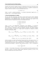
structure is shown in Fig.1.
4
Advances in Optical Amplifiers
Fig. 1. Structure of SOA
SOA can operate in two different regimes. In the first case called the travelling-Wave (TW)
regime, the oscillations are prevented in order to create a single pass gain , Eisenstein (1989),
Agrawal (2002). The active medium is described as a homogeneously broadened two-level
system. In such a case, the gain coefficient g
(
ω
)
has the form Agrawal (2002)
g
(
ω
)
=
g
0
1 +
(
ω −ω
0
)
2
T
2
2
+ P/P
s
(1)
where g
0
is the peak value of the gain, ω
0
is the transition frequency, P is the optical power
of the amplified signal, P
s
is the saturation power, and T
2
≤ 1ps is the dipole relaxation time.
Under the condition of P/P
s
1 corresponding to the unsaturated regime, equation (1) takes
the form
g
(
ω
)
=
g
0
1 +
(
ω −ω
0
)
2
T
2
2
(2)
It is seen from equations (1) and (2) that the frequency dependence of the gain is characterized
by a Lorentzian profile with the resonance frequency ω
0
. The gain bandwidth Δω
g
defined as
the full width at half maximum (FWHM) is given by Agrawal (2002).
Δω
g
=
2
T
2
(3)
The local optical power P
(
z
)
in a gain medium can be defined as Agrawal (2002).
P
(
z
)
=
P
(
0
)
exp
(
gz
)
(4)
where P
(
0
)
=
P
in
is the input optical power. We can define an amplification factor G
(
ω
)
for
a SOA of length L as the ratio between the output optical power P
out
= P
(
L
)
and P
in
Agrawal
(2002).
G
(
ω
)
=
P
out
P
in
=
P
(
L
)
P
(
0
)
=
exp
(
gL
)
(5)
The gain saturation regime is defined by the gain dependence on the optical power according
to equation (1). It can be shown that for the large-signal amplification factor the following
5
Semiconductor Optical Amplifiers
relationship prevails Agrawal (2002).
G
= G
0
exp
−
(
G − 1
)
P
out
GP
s
(6)
where G
0
is the unsaturated amplification factor. The main noise in SOA is due to the
spontaneous emission. The SNR degradation is characterized by the amplifier noise figure
(NF) F
n
defined by Agrawal (2002).
F
n
=
(
SNR
)
in
(
SNR
)
out
(7)
NF can reach 6
− 8dB. However for optical communication applications it should be as low
as possible Agrawal (2002).
In the second regime, called Fabry-Perot (FP) SOA, a semiconductor laser biased slightly
below threshold is used as SOA in a FP cavity where the FP cavity is characterized by
multiple reflections at the facets with reflectivities R
1,2
Agrawal (2002). The amplification
factor G
FP
(
ω
)
for such a FP SOA is given by Agrawal (2002)
G
FP
(
ν
)
=
(
1 − R
1
)(
1 − R
2
)
G
1
− G
√
R
1
R
2
2
+ 4G
√
R
1
R
2
sin
2
[
π
(
ν − ν
m
)
/Δν
L
]
(8)
where ν
= ω/2π, ν
m
= mc/2nL are the cavity resonance frequencies, c is the free space
light velocity, Δν
L
= c/2nL is the longitudinal mode spacing, and m = 1, 2,3, is the mode
number. The FP SOA bandwidth Δν
A
at the 3dB level of G
FP
(
ν
)
is given by Agrawal (2002)
Δν
A
=
2Δν
L
π
arcsin
1
− G
√
R
1
R
2
4G
√
R
1
R
2
1/2
(9)
2.2 Rate equations and optical field propagation equations
The efficiency of SOA applications in all-optical integrated circuits for optical signal
processing and functional devices is mainly determined by their high gain coefficient and
a relatively low saturation power Agrawal (1989), Agrawal (2002), Premaratne (2008). Device
engineering and performance optimization require simple and quantitatively accurate models
for SOAs providing an adequate description of SOAs peculiarities Premaratne (2008).
The theory of pulse propagation in amplifiers based on a two-level system model is also
valid for SOAs Agrawal (1989). The SOA’s active region is modeled as an ensemble of
noninteracting two-level systems with transition energies extending over the range of the
conduction and valence bands Agrawal (1989). If the pulse width T
p
1ps is much larger
than the intraband relaxation time τ
in
∼ 0.1ps and, on the other hand, T
p
τ
e
∼ 10
−10
s
where τ
e
is the carrier lifetime, the rate-equation approximation can be applied where the
amplification process within the SOA is described by the following rate equations for the
carrier density N
(
z, t
)
and the optical signal intensity I
(
z, t
)
Agrawal (1989), Agrawal (2002),
Premaratne (2008).
∂N
(
z, t
)
∂t
= ρ
(
z
)
−
N
(
z, t
)
τ
e
− g
(
z, t
)
λI
(
z, t
)
hc
(10)
∂I
(
z, t
)
∂z
+
1
v
g
∂I
(
z, t
)
∂t
= g
(
z, t
)
I
(
z, t
)
−
αI
(
z, t
)
(11)
6
Advances in Optical Amplifiers
where t is the time, z is the distance along the light propagation direction in the SOA
active region, ρ
(
z
)
is the current-injection density, α is the loss coefficient, λ is the operating
wavelength, and h is the Planck’s constant. The input pulse intensity profile I
0
(
t
)
is given by
Premaratne (2008)
E
g
= A
m
∞
−∞
I
0
(
t
)
dt (12)
where A
m
is the effective mode area of the SOA active region, and E
g
is the pulse energy. The
gain coefficient g
(
z, t
)
is defined as Premaratne (2008).
g
(
z, t
)
=
Γa
[
N
(
z, t
)
−
N
0
]
where Γ is the mode confinement factor, a is the differential gain coefficient, and N
0
is the carrier density corresponding to the transparency state. By using the coordinate
transformations z, τ
= t −z/v
g
and introducing the new variable
h
(
z, τ
n
)
=
z
0
g
(
z, τ
)
dz (13)
where z
⊂
[
0, L
]
, τ
n
=
τv
g
/L is normalized time, and L is the length of SOA, equations
(10) and (11) can be reduced to the following integro-differential equation describing the gain
recovery dynamics for a short optical pulse Premaratne (2008)
∂h
(
z, τ
n
)
∂τ
n
=
h
ρ
− h
(
z, τ
n
)
− β
(
τ
n
)
{
exp
[
h
(
z, τ
n
)
−
αz
]
−
1
}
−
β
(
τ
n
)
⎡
⎣
α
z
0
exp
[
h
(
z, τ
n
)
−
αz
]
dz
⎤
⎦
(14)
where
= L/
v
g
τ
e
, β
(
τ
n
)
=
ΓaλI
0
(
τ
)
L/
v
g
hc
, and
h
ρ
(
z
)
=
z
0
[
τ
e
Γaρ
(
z
)
−
ΓaN
0
]
dz (15)
Equation (14) has been solved analytically and numerically for different situations using a
multiple-scales technique Premaratne (2008). In particular, the signal gain G
(
z, T, U
)
is given
by Premaratne (2008).
G
(
z, T, U
)
exp
(
−
αz
)
=
exp
{
[
h
(
z
)
−
αz
][
1 −exp
(
−
U
)]
}
×
1
−
1 −exp
(
−
h
I
(
z
)
+
αz
)
E
γ
(
T
)
−exp
(
−
U
)
(16)
where T = τ
n
is the pulse time scale, U = τ
n
is a slow time scale corresponding to the carrier
recovery, and h
I
(
z
)
is the initial profile of h
(
z, T, U,
)
,
E
γ
(
T
)
=
exp
⎛
⎝
T
0
β
(
T
)
g
(
z, T, U
)
[
g
(
z, T, U
)
−
α
]
dT
⎞
⎠
(17)
7
Semiconductor Optical Amplifiers
g
(
z, T, U
)
=
h
ρ
(
z
)
z
[
1 −exp
(
−
U
)]
−
exp
(
−
U
)
z
×ln
1 −
(
1 −exp
(
−
h
I
(
z
)))
E
β
(
T
)
(18)
and
E
β
(
T
)
=
exp
⎛
⎝
T
0
β
(
T
)
dT
⎞
⎠
(19)
The electric field E
(
z, t
)
of the pulse is given by Premaratne (2008)
E
(
z, t
)
=
I
(
z, t
)
exp
[
i
(
φ
(
z, t
)
−
ωt
)]
; φ
(
z, t
)
=
α
L
2
h
(
z, t
)
(20)
where φ
(
z, t
)
is the phase of the pulse inside SOA and α
L
is the linewidth enhancement factor
(LEF).
Comparison of the analytical results of the theory developed above with the numerical
simulation results for Gaussian picosecond pulses propagating through a SOA of length L
≈ 400μm , active region width and thickness of 2.5μm and 0.2μm, respectively, Γ = 0.3, carrier
injection rate 1.177
×10
34
s
−1
m
−3
, n
g
= 3.7, α = 3000m
−1
, τ
e
= 3 ×10
−10
s, a = 2.5 ×10
−20
m
2
,
N
0
= 1.5 ×10
24
m
−3
, α
L
= 5, and λ = 1552.52nm shows a good accord Premaratne (2008).
3. Advanced structures
3.1 QW SOA
The structure of QW SOA devices is very similar to that of bulk SOA, except that the active
layer thickness of the former is reduced to the order of 10nm where quantum effects play
an essential role. A thin layer sandwiched between two layers of a wide band gap material
form a finite potential well. As a consequence of carriers confinement in the z direction in the
thin layer, the conduction and valence bands break up into a series of well-defined sub-bands
with a step-like density of states (DOS) function ρ
QW
(
E
)
which is energy independent. DOS
function for electrons has the form Zhao (1999)
ρ
QW
(
E
)
=
∑
n
e
m
e
π¯h
2
H
[
E
e
− E
ez
(
n
e
)]
(21)
where m
e
is the electron effective mass, ¯h = h/
(
2π
)
, E
e
is the total electron energy given by
E
e
= E
ez
(
n
e
)
+
(
¯hk
)
2
2m
e
(22)
E
ez
(
n
e
)
are the quantized energy levels, n
e
= 1, 2, is the level number, k =
k
2
x
+ k
2
y
is
the electron wave vector corresponding to the motion in the
(
x, y
)
directions, and H
[
x
]
is the
Heaviside function given by
H
[
x
]
=
1, x
≥ 0
0, x
< 0
(23)
8
Advances in Optical Amplifiers
There is no quantum confinement in the
(
x, y
)
plane. The quantized electron energies E
ez
(
n
e
)
can be evaluated by solving the Schrödinger equation for the case of the confinement in the z
direction Zhao (1999)
−
¯h
2
2m
e
∂
2
∂z
2
+ V
(
z
)
Φ
n,k
(
z
)
=
E
n
Φ
n,k
(
z
)
(24)
where
E
n
= E
ez
(
n
e
)
+
E
n0
+
(
¯hk
)
2
2m
e
(25)
V
(
z
)
is the confinement potential, and the electron wave function Ψ
n
(
x, y, z
)
is given by Zhao
(1999)
Ψ
n
(
x, y, z
)
=
u
n
(
x, y, z
)
Φ
n,k
(
z
)
1
L
x
L
y
exp i
k
x
x + k
y
y
(26)
Here, u
n
(
x, y, z
)
is the periodic Bloch function, L
x
and L
y
are the SOA dimensions in the
(
x, y
)
directions, respectively. In the simplest case of a finite square-well potential V
0
, the energy
spectrum of QW is determined by the solutions of the following transcendental equations
Brennan (1999).
k
1
= k
2
tan
k
2
d
z
2
; k
1
= −k
2
cot
k
2
d
z
2
(27)
where
k
1
=
2m
e
(
V
0
− E
)
¯h
2
;k
2
=
2m
e
E
¯h
2
; (28)
and d
z
is the QW dimension in the z direction.
In this structure stimulated emission occurs only between discrete energy levels. QW-SOAs
have superior performance as compared to bulk SOAs in terms of optical bandwidth and
maximum output power. In SOAs, the saturation output power is inversely proportional to
the differential gain coefficient, which is smaller in QW-SOAs.
The conventional SOA has rather poor carrier and photon confinement. Optical confinement
can be enhanced by the implementation of a tapered graded index (GRIN) region on both
sides of the well. A multi quantum well SOA (MQW-SOA) can be produced by stacking
several layers of wells and barriers, usually created by molecular beam epitaxy (MBE) and/or
metal organic vapor deposition (MOCVD) techniques. The optical gain of MQW is higher due
to multiple QWs. Further improvement of the SOA performance is achieved by introducing
an outer cladding region of a higher energy gap compared to the MQW barrier layers. The
optical confinement factor of MQW SOAs increases approximately linearly with the number
of QWs.
Many applications of SOA such as optical amplification, optical switching and signal
processing require gain and phase shift insensitivity to the polarization. The polarization
dependence of the phase shift is due to intrinsic or induced birefringence in SOA, so that
the effective refraction index for the transverse electric (TE) mode is different from that
of the transverse magnetic (TM) mode. These dependencies stem, in turn, from different
quantization levels for heavy-hole (HH) bands, which provide the TE-mode dominant optical
gain, and light-hole (LH) bands, which provide the TM-mode dominant optical gain. The
difference in the confinement factors for TE and TM modes leads to different TE and TM
signal gains.
9
Semiconductor Optical Amplifiers