Advances in Photodiodes Part 7 pptx
Bạn đang xem bản rút gọn của tài liệu. Xem và tải ngay bản đầy đủ của tài liệu tại đây (3.87 MB, 30 trang )
Color-Selective CMOS Photodiodes Based on Junction Structures and Process Recipes
169
(d)
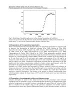
Fig. 11. Measured spectral responses of photodiodes under different reverse biased voltages
in (a) n-/p-sub, (b) p
+
/n-/p-sub,(c) n-/p-epi/p+sub and (d) p
+
/n
(a)
(b)
Fig. 12. Variations in positions of the space-charge regions of (a) n-/p-sub photodiode and
(b) p
+
/n- photodiodes, at reverse bias voltages from 0V to -5V (the dimensions of each layer
in this structure do not represent actual dimensions).
Advances in Photodiodes
170
spectral response. Figure 13(b) shows the simulated spectral responses of n-, space-charge,
p-substrate regions, and the total spectral responses at reverse biased voltages from 0V to -
5V when the reflection coefficient is zero. The variation of the spectral response for this
photodiode increases with the reverse biased voltage more significantly than those in the
other three photodiodes.
(a)
(b)
Fig. 13. Simulated spectral responses in n-type and p-type semiconductors and in space-
charge region under different reverse biased voltages ranging from 0V to -5V when the
reflection coefficient being zero for (a) n-/p-sub and (b) p
+
/n- photodiodes.
Color-Selective CMOS Photodiodes Based on Junction Structures and Process Recipes
171
4. Design methodology for color CMOS pixels without color filters
As the abovementioned, we conclude that the color filter technology is still a good choice for
color separation presently. In fact, some specific modifications for the semiconductor
process or signal processing circuits are applied to color CMOS image sensors without color
filters [15]-[17]. In this work, an equation based on the CMOS photodiode model is derived
to determine the peak wavelength of the spectral response. The detail of the derivation
procedure is illustrated in Appendix. Here, some solutions for obtaining different color
spectral responses are briefly sketched. Additionally, the approaches to enhance the
capability of separating the color spectral responses are discussed.
1. Reducing the spectral response in the long wavelength region:
Generally, the thickness of the substrate is as thick as several hundreds of micrometers.
Consequently, the spectral response is dominated by the induced photocurrent
generated in the substrate region. Since the peak wavelength of the spectral response of
substrate is generally located at the infrared region, the peak wavelength of the total
spectral response tends to occur at the long wavelength region. There are two
approaches to reduce the spectral response in the long wavelength region.
a. The spectral responses in the long wavelength region can be effectively decreased by
shortening the p-n junction in the deep region [16]. The depth of diffusion affects the
photodiode to absorb wavelengths of incident light. Referring to the absorption
length in Fig. 7, the light with a longer wavelength penetrates to the deeper junction
so that the incident light with a longer wavelength can excite electron-hole pairs at
the deep region. However, to become photocurrents, the electron-hole pairs should
reach to the boundary edges of the space-charge region successfully such that they
would be absorbed and transformed to the photocurrent. In other words, the
photodiode has a greater response toward the incident light with a longer
wavelength at a deeper region whereas for a shallower region it has a better response
toward the incident light with a shorter wavelength. Additionally, to prevent CMOS
circuits from latch-up, p-substrate is generally connected to the lowest potential in the
system. To keep the potential of p-substrate in the lowest level and the photodiode
under reverse biased voltages, a connection manner depicted in Fig. 14 is employed
to solve the problem of the voltage drop between p and n nodes in the photodiode.
Figure 15 shows the simulated results utilizing the recipes in Fig. 14. It clearly reveals
that the peak wavelength increases with the depth of the p
+
layer.
Fig. 14. Connection manner, recipes and structures obtaining three color spectral responses.
Advances in Photodiodes
172
(a)
(b)
Fig. 15. Structures in Fig. 14 being simulated to yield (a) spectral responses of three recipes
for red, green and blue photodiodes and (b) spectral responses of p
+
depth varying from
0.1μm to 2.1μm.
b. The spectral response in the long wavelength region can be also lowered by
reducing the thickness of the substrate layer to decrease the region for collecting
excess minority carriers. Figure 16 depicts the n-/p-sub photodiode with thin p-
substrate of which the thickness is only several micrometers. Figure 17 displays the
simulated results by utilizing the corresponding recipes in Fig. 16. It is apparent
that the spectral response in the long wavelength region is decayed.
Color-Selective CMOS Photodiodes Based on Junction Structures and Process Recipes
173
p-substrate : 1X10
15
cm
-3
n- : 1X10
15
cm
-3
Red Photodiode
6.5um
p
+
n
+
5.8um
n- : 1X10
15
cm
-3
Red Photodiode
n
+
3.5um
n- : 1X10
15
cm
-3
Blue Photodiode
n
+
0.7um
Fig. 16. Structures in Fig. 16 being simulated to yield (a) spectral responses of three recipes
for red, green and blue photodiodes and (b) spectral responses of n﹣depth varying from
0.7μm to 5.8μm.
(a)
(b)
Fig. 17. Simulated results employing the structures in Fig. 16 under different recipes.
Advances in Photodiodes
174
(a)
(b)
Fig. 18. Simulated spectral responses of the n-/p-epi/p+sub photodiode in (a) p-epitaxial
doping concentration of 1×10
15
cm
-3
and p-epitaxial thickness ranging from 5 to 15 um um
and (b) p-epitaxial doping concentration ranging from 1×10
15
cm
-3
to 1×10
19
cm
-3
and p-
epitaxial thickness of 10
um .
Color-Selective CMOS Photodiodes Based on Junction Structures and Process Recipes
175
2. The spectral response in the long wavelength region can be decreased by heavy doping
substrate associated with the p-epitaxial layer. By adjusting the depth of the epitaxial
layer, the desired spectral response can be obtained. Figure 18 depicts the simulated
spectral responses of the n-/p-epi/p+sub photodiode under different thicknesses and
doping concentrations of the epitaxial layer. According to this figure, the thickness and
doping concentration of the epitaxial layer apparently affect spectral responses. In
practice, some researchers proposed the approach of selective epitaxial growth to obtain
various color spectral responses by changing the recipe of the epitaxial layer [20], [21].
5. Conclusion
Adaptive photodiode structures, of which design approach aiming at making the photo-
response having a peak value at a specific wavelength, that are realized by the photodiodes
with color-selective mechanisms under the condition of without extra color filters is
proposed. Moreover, the influences of color filters, photodiode structures, recipes and
reverse biased voltages on spectral responses are investigated. Measurement results
illustrate that the color filters affect the spectral responses more significantly than the others.
The spectral response varies with the reverse biased voltages slightly. The approach of
implementing color pixels using the standard CMOS process without color filters is also
proposed. This work clearly paves the way for designers to realize color-selective pixels in
CMOS image sensors.
Appendix: Derivation for peak wavelength of the spectral response
The n-/p-sub photodiode as shown in Fig. A.1 is employed to illustrate how the proposed
model is used to derive the peak wavelength of the spectral response.
Fig. A.1 n-/p-sub photodiode.
The total current density generated by the n-/p-sub photodiode is
Advances in Photodiodes
176
()()
()
2
12
1
1
11
0
22
11
() ()
1
total n photo p photo drift
x
p n photo n sub p sub photo x
xx xx
x
x
pp
p
p
pp p p p
pp
p
p
p
pp
JJ J J
qD dp x dx qD dn x dx q G dx
DS
D
exx
sh S ch
LL L L L
qD G
L
D
xx
Ssh ch
LL
α
α
τ
α
−−
−−−
==
−
=++
=+ +
⎛⎞
⎛⎞
+
⎛⎞ ⎛⎞
⎜⎟
⎜⎟
⎜⎟ ⎜⎟
+−
⎜⎟ ⎜⎟
⎜⎟
⎜⎟
⎝⎠ ⎝⎠
⎝⎠
⎝⎠
=
−
⎛⎞
⎜⎟
+
⎜⎟
⎝⎠
∫
()()
()
()
1
23 23
2
21
2
2
23 23
0
22
0
1
x
p
xx xx
x
nsub nsub
nsub nsub
nsub
xx
e
L
xx xx
qL G e e L Coth e Csch
LL
L
qe e
α
αα
α
αα
α
α
α
φ
−
−+ +
−−
−−
−
−−
⎛⎞
⎜⎟
⎜⎟
⎜⎟
+
⎜⎟
⎛⎞
⎛⎞
⎜⎟
⎜⎟
⎜⎟
⎜⎟
⎜⎟
⎜⎟
⎜⎟
⎝⎠
⎝⎠
⎝⎠
⎛⎞
⎛⎞
⎛⎞ ⎛⎞
−−
⎜⎟
+−
⎜⎟
⎜⎟ ⎜⎟
⎜⎟
⎜⎟
⎝⎠ ⎝⎠
⎝⎠
⎝⎠
+
−
+−
.(A1)
The absorption coefficient
α
can be simplifily represented as a function of the incident light
wavelength, i.e.
(
)
f
α
λ
= , and then Eq. (A1) can be modified to
()
()
()
(
)
()
()
()
()
1
1
2
11
0
2
2
11
23
0
1
fx
pp
p
p
ppp p p
pp
fx
total
p
p
p
pp p
xf
nsub nsub
nsu
fDS
D
exx
sh S ch
LLL L L
qD G
J fe
Lf
D
xx
Ssh ch
LL L
xx
qL G e f L Coth
L
λ
λ
λ
λ
τ
λ
λ
λ
−
−
−
−−
−
⎛⎞
⎛⎞
⎛⎞
+
⎛⎞ ⎛⎞
⎜⎟
⎜⎟
⎜⎟
⎜⎟ ⎜⎟
+−
⎜⎟
⎜⎟ ⎜⎟
⎜⎟
⎜⎟
⎝⎠ ⎝⎠
⎝⎠
⎜⎟
⎝⎠
=+
⎜⎟
⎛⎞
⎛⎞ ⎛⎞
−
⎜⎟
⎜⎟
⎜⎟ ⎜⎟
+
⎜⎟
⎜⎟ ⎜⎟
⎜⎟
⎜⎟
⎝⎠ ⎝⎠
⎝⎠
⎝⎠
−
+
+
()
()
(
)
() ()
(
)
3
21
23
2
2
0
1
xf
bnsub
nsub
fx fx
xx
eCsch
L
Lf
qe e
λ
λλ
λ
φ
−
−
−
−−
⎛⎞
⎛⎞
⎛⎞ ⎛⎞
−
⎜⎟
−
⎜⎟
⎜⎟ ⎜⎟
⎜⎟
⎜⎟
⎝⎠ ⎝⎠
⎝⎠
⎝⎠
−
+−
. (A2)
In Eq. (A2), the surface generation rate
0
G is
(
)
0
in
in
fP
P
G
Ahc Ahc
λ
λ
αλ
== . (A3)
Additionally,
A and P
in
in Eq. (A3) represent the unit area and unit incident light power,
respectively. Hence, Eq. (A2) can be represented as follows.
Color-Selective CMOS Photodiodes Based on Junction Structures and Process Recipes
177
()
()
(
)
()
()
(
)
()
()
()
()
(
)
()
()
1
1
2
11
2
2
11
2
2
1
1
fx
pp
p
p
ppp p p
pp
fx
total
p
p
p
pp p
xf
nsub
n
nsub
fDS
D
exx
sh S ch
LLL L L
qD f
J fe
D
hc L f
xx
Ssh ch
LL L
qL f
efL
hc L f
λ
λ
λ
λ
τλλ
λ
λ
λλ
λ
λ
−
−
−
−
−
−
⎛⎞
⎛⎞
⎛⎞
+
⎛⎞ ⎛⎞
⎜⎟
⎜⎟
⎜⎟
⎜⎟ ⎜⎟
+−
⎜⎟
⎜⎟ ⎜⎟
⎜⎟
⎜⎟
⎝⎠ ⎝⎠
⎝⎠
⎜⎟
⎝⎠
=+
⎜⎟
⎛⎞
⎛⎞ ⎛⎞
−
⎜⎟
⎜⎟
⎜⎟ ⎜⎟
+
⎜⎟
⎜⎟ ⎜⎟
⎜⎟
⎜⎟
⎝⎠ ⎝⎠
⎝⎠
⎝⎠
+
−
()
() ()
(
)
3
21
23 23
0
xf
sub
nsub nsub
fx fx
xx xx
Coth e Csch
LL
qe e
λ
λλ
φ
−
−−
−−
⎛⎞
⎛⎞
⎛⎞ ⎛⎞
−−
⎜⎟
+−
⎜⎟
⎜⎟ ⎜⎟
⎜⎟ ⎜⎟
⎜⎟
⎜⎟
⎝⎠ ⎝⎠
⎝⎠
⎝⎠
+−
(A4)
The peak wavelength of the spectral response can be obtained by taking partial differential
of Eq. (A4) by the variable of
λ
.
()
() ()
(
)
()
()
() () ()
(
)
()
()
(
)
() ()
(
)
()
()
() ()
()
()
()
()
(
)
() () ()
()
(
)
( )
1
22
22
2
2
2
11
2 22
2 2
1
111
1'2
1
1'2 111
total
fx
pppp pppp
pppp
pp
ppppppp
p
p
J
e Lf f L f DS f f DS f LS
xx
Lf DCosh LSSinh
LL
x
LCosh f f L fDS f fD fxf L S fxf fx
L
qL
hc
λ
λ
λλ λ λλ λ λ
λ
λλ λ λλ λ λ λ λ λ λ
−
∂
=
∂
−+− ++
⎛⎞
⎛⎞ ⎛⎞
⎜⎟
⎜⎟ ⎜⎟
−+
⎜⎟ ⎜⎟
⎜⎟
⎝⎠ ⎝⎠
⎝⎠
⎛⎞
⎛
⎜⎟
−−++ + −+−++
⎜⎟
⎝
⎝⎠
=+
()
(
)
() ()
(
)
()
()
() () () ()
()
(
)
() () ()
(
)
()
()
(
)
2
2
2
11
2 22
22 2 2 2
1
11 1
2
2
2
11
1
1'11 21
1
pppp
pp
pp pp p p pp p
p
pppp
pp
xx
L f DCosh LSSinh
LL
x
Sinh f f L D f L S f D f x f L f x f L S f x f L
L
xx
Lf DCosh LSSinh
LL
λ
λλ λ λλ λ λ λ λ λ λ
λ
⎞
⎜ ⎟
⎠
⎛⎞
⎛⎞ ⎛⎞
⎜⎟
⎜⎟ ⎜⎟
−+
⎜⎟ ⎜⎟
⎜⎟
⎝⎠ ⎝⎠
⎝⎠
⎛⎞
⎛ ⎞
⎛⎞
⎜⎟
−−++−++++ −
⎜⎟
⎜ ⎟
⎜⎟
⎝⎠
⎝ ⎠
⎝⎠
+
⎛⎞ ⎛
⎜⎟
−+
⎜⎟
⎝⎠ ⎝
()
()
()
()
()
()
()
(
)
() ()
()
()
()
22 3
22
2
23 23
2
2
23
1
''
fx fx fx
nsub
nsub nsub
nsub
fx fx
nsub
n
nsub
xx xx
Lf e fe Coth fe Csch
LL
Lf
xx
L ffe fe Coth
L
qL
hc
λλ λ
λλ
λλ λ
λ
λλ λ λ λ
−− −
−
−−
−
−−
−
−
⎛ ⎞
⎜ ⎟
⎜ ⎟
⎜ ⎟
⎜ ⎟
⎜ ⎟
⎜ ⎟
⎜ ⎟
⎜ ⎟
⎜ ⎟
⎜ ⎟
⎜ ⎟
⎜ ⎟
⎜ ⎟
⎜ ⎟
⎜ ⎟
⎜ ⎟
⎜ ⎟
⎜ ⎟
⎜ ⎟
⎛⎞
⎞
⎜ ⎟
⎜⎟
⎜⎟
⎜ ⎟
⎜⎟
⎜⎟
⎜ ⎟
⎠
⎝⎠
⎝ ⎠
⎛⎞ ⎛⎞
−−
+−
⎜⎟ ⎜⎟
⎝⎠ ⎝⎠
−
−
+
+
+
()
()
()
(
)
() ()
()
() ()
()
() () () ()
()
()
(
)
() ()
()
()
3
22 3
2
23
2
2
2
23 23
22 3
2
2
3
3
'
1
''''
1
2'2
fx
sub n sub
nsub
fx fx fx
nsub nsub
nsub nsub
nsub
fx
nsub
xx
fe Csch
L
Lf
xx xx
L ffe Lxf fe xffCoth xffe Csch
LL
Lf
Lffe f
λ
λλ λ
λ
λλ
λ
λλ λ λλ λ λλ λ λλ λ
λ
λλ λ λλ
−
−−
−
−− −
−−
−−
−
−
−
⎛⎞ ⎛⎞
−
−
⎜⎟ ⎜⎟
⎝⎠ ⎝⎠
−
⎛⎞ ⎛⎞
−−
−−+
⎜⎟ ⎜⎟
⎝⎠ ⎝⎠
+
−
+
−
()
()
() ()
()
()
(
)
()( ) ()
()
()
()
()
()
(
)
()
2 3
12 2 1
22
22
23 23
2
2
2
12
'2'
1
'1 '1
fx fx
nsub nsub
nsub nsub
nsub
fxx fx fx
xx xx
fLe Coth f fLe Csch
LL
Lf
q
eefxefx
hc
λλ
λλ λ
λλλλ
λ
λλ λλ
−−
−−
−−
−
−+
⎛ ⎞
⎜ ⎟
⎜ ⎟
⎜ ⎟
⎜ ⎟
⎜ ⎟
⎜ ⎟
⎜ ⎟
⎜ ⎟
⎜ ⎟
⎜ ⎟
⎜ ⎟
⎜ ⎟
⎜ ⎟
⎜ ⎟
⎜ ⎟
⎜ ⎟
⎜ ⎟
⎛⎞ ⎛⎞
−−
⎜ ⎟
−
⎜⎟ ⎜⎟
⎜ ⎟
⎝⎠ ⎝⎠
⎜ ⎟
⎜ ⎟
−
⎜ ⎟
⎝ ⎠
+−+−
(A5)
The calculation result represents the slope of Eq. (A4). When Eq. (A5) equals to 0, the
corresponding
λ
is the peak wavelength of the spectral response.
Equation (A5) is a complex non-exact differential equation. Accordingly, some assumptions
are employed to simplify the solution for Eq. (A5). The spectral response induced in the
Advances in Photodiodes
178
space-charge region is generally too small to be neglected. Additionally, diffusion lengths of
the minority carriers in n- and p-substrate are as long as several hundred micrometers
owing to low-doped concentrations, and thus wavelengths in the visible region are much
smaller than the diffusion lengths. Moreover, there exist the following assumptions
() ()
22
22
1
pp
Lf Lf
λ
λ
−≅ , (A6)
() ()
22
22
1
nsub nsub
Lf Lf
λ
λ
−−
−≅ , (A7)
and
1p
Lx>> . (A8)
Eq. (A5) can be simplified as follows.
()
() ()
()
()
()
() ()
()
()
()
()
()
() () () () () () ()
() () () () () () ()
()
()
()
11 1 1
1
2
2
44 3
22
2334
1
2
23 4
11
22 2
4
4
1
2' '
'2'''
'''
1
1
pp
fx fx fx fx
p
ppp
pp p
fx
pp
pp
pp p
fx
pp pp pp
fx
nsub
SS
ffe fe ffe fe
D
LLD
SS S
fe f f f f ffxf
DD
LD
SS S
ffx f f f fx f e
LD LD LD
fe
Lf
f
λλ λ λ
λ
λ
λ
λλ λ λλλ λλ
λ λλ λ λλ λλλ λ λλ
λλ λ λλ λ λλ λ λ
λ
λ
−− − −
−
−
−
−
++ − −
−++++−
++ +
+
()
()
()
() ()
()
() ()
()
() ()
()
() ()
()
() ()
()
()
3 2
2 3
22
33
23 23
22
23 23
34
2
1
'
11
''
''
fx fx
nsub nsub nsub
fx fx
n sub n sub n sub n sub
fx fx
xx xx
Coth f e Csch f f e
LLL
xx xx
ffe Coth ffe Csch
LL LL
ffe ffe xf
λλ
λλ
λλ
λλλλ
λ
λλ λ λλ λ
λλ λ λλ λ λλ
−−
−−−
−−
−− −−
−−
⎛⎞ ⎛⎞
−−
−+
⎜⎟ ⎜⎟
⎜⎟ ⎜⎟
⎝⎠ ⎝⎠
⎛⎞ ⎛⎞
−−
+−
⎜⎟ ⎜⎟
⎜⎟ ⎜⎟
⎝⎠ ⎝⎠
+− −
()
()
() ()
()
()
() ()
()
() ()
()
() ()
()
3 2
2 3
4
23
2
43
23
3
22
23 23
1
'
1
'2'
11
2' 2' 0
nsub nsub
fx fx
n sub n sub
fx fx
nsub nsub nsub nsub
xx
fx Coth
Lf L
xx
ffe x Csch ffe
Lf L
xx xx
ffe Coth ffe Csch
LL LL
λλ
λλ
λ
λ
λλ λ λλ λ
λ
λλ λ λλ λ
−−
−−
−−
−−
−− −−
⎛
⎜
⎜
⎜
⎜
⎜
⎛⎞
−
⎜⎟
⎜⎟
⎝⎠
⎛⎞
−
+−
⎜⎟
⎜⎟
⎝⎠
⎛⎞ ⎛⎞
−−
−+ =
⎜⎟ ⎜⎟
⎜⎟ ⎜⎟
⎝⎠ ⎝⎠
⎝
⎞
⎟
⎟
⎟
⎟
⎟
⎜ ⎟
⎜ ⎟
⎜ ⎟
⎜ ⎟
⎜ ⎟
⎜ ⎟
⎜ ⎟
⎜ ⎟
⎜ ⎟
⎜ ⎟
⎜ ⎟
⎜ ⎟
⎜ ⎟
⎜ ⎟
⎜ ⎟
⎜ ⎟
⎜ ⎟
⎜ ⎟
⎜ ⎟
⎜ ⎟
⎜ ⎟
⎜ ⎟
⎠
(A9)
6. Acknowledgement
This work was partially supported by National Science Council, Taiwan, under the contract
number of NSC 97-2221-E-194-060-MY3.
7. References
[1] B. E. Bayer, “Color Imaging Array,” U. S. Patent 3971065, July 1976.
[2] W. J. Liu, Oscal T C. Chen, L. K. Dai, P. K. Weng, K. H. Huang and Far-Wen Jih, “A
CMOS photodiode model,” Proc. of IEEE International Workshop on Behavioral
Modeling and Simulation, pp. 102-105, 2001.
[3] K. C. Chang, C. Y. Chang, Y. K. Fang and S. C. Jwo, “The amorphous Si/SiC
heterojunction color-sensitive phototransistor,” IEEE Electron Device Letters, vol. 8,
no. 2, pp. 64-65, 1987.
Color-Selective CMOS Photodiodes Based on Junction Structures and Process Recipes
179
[4] H. K. Tsai, S. C. Lee and W. L. Lin, “An amorphous SiC/Si two-color detector,” IEEE
Electron Device Letters, vol. 8, no. 8, pp. 365-367, 1987.
[5] Y. K. Fang, S. B. Hwang, K. H. Chen, C. R. Liu, M. J. Tsai and L. C. Kuo, ”An amorphous
SiC/Si heterojunction p-i-n diode for low-noise and high-sensitivity UV detector,”
IEEE Trans. on Electron Devices, vol. 39, no. 2, pp. 292-296, 1992.
[6] Y. K. Fang, S. B. Hwang, K. H. Chen, C. R. Liu, M. J. Tsai and L. C. Kuo,”A metal-
amorphous silicon-germanium alloy Schottky barrier for infrared optoelectronic IC
on glass substrate application,” IEEE Trans. on Electron Devices, vol. 39, no. 6, pp.
1348-1354, 1992.
[7] G. de Cesare, F. Irrera, F. Lemmi and F. Palma, “Tunable photodetectors based on
amorphous Si/SiC heterostructures,” IEEE Trans. on Electron Devices, vol. 42, no. 5,
pp. 835-840, 1995.
[8] K. Eberhardt, T. Neidlinger and M. B. Schubert, “Three-color sensor based on amorphous
n-i-p-i-n layers sequence,” IEEE Trans. on Electron Devices, vol. 42, no. 10, pp. 1763-
1768, 1995.
[9] J. Zimmer, D. Knipp, H. Stiebig and H. Wagner, “Amorphous silicon-based unipolar
detector for color recognition,” IEEE Trans. on Electron Devices, vol. 46, no. 5, pp.
884-891, 1999.
[10] M. Topic, H. Stiebig, D. Knipp and F. Smole, ”Optimization of a-Si:H-based three-
terminal three-color detectors,” IEEE Trans. on Electron Devices, vol. 46, no. 9, pp.
1839-1845, 1999.
[11] T. Su, P. C. Taylor, G. Ganguly and D. E. Carlson, “Direct role of hydrogen in the
Staebler-Wronski effect in hydrogenated amorphous silicon,” Physical Review
Letters, vol. 89, no. 1, pp. 015502-1-015502-4, 2002.
[12] T. Lule, M. Wagner, M. Verhoeven, H. Keller and M. Bohm, “100000-pixel, 120-dB
imager in TFA technology,” IEEE Journal of Solid-State Circuits, vol. 35, no. 5, pp.
732-739, 2000.
[13] Masahiro Kasano, Yuichi Inaba, Mitsuyoshi Mori, Shigetaka Kasuga, Takahiko Murata
and Takumi Yamaguchi, “A 2.0-μm pixel pitch CMOS image sensor with 1.5
transistor/pixel and an amorphous Si color filter,” IEEE Trans. on Electron Devices,
vol. 53, no. 4, pp. 611-617, 2006.
[14] Foveon Inc, “Color separation in an active pixel cell imaging array using a triple-well
structure,” U.S. Patent 5 965 875, 12 Oct. 1999.
[15] K. M. Findlater, D. Renshaw, E. D. Hurwitz, R. K. Henderson, M. D. Percell, S. G. Smith
and T. E. R. Bailey, ”A CMOS image sensor with a double-junction active pixel,”
IEEE Trans. on Electron Devices, vol. 50, no.1, Jan. 2003.
[16] W. J. Liu, O. T C. Chen, L. K. Dai, P. K. Weng, K. H. Huang and F. W. Jih, “A color
image sensor using adaptive color pixels,” Proc. of IEEE Midwest Symposium on
Circuits and Systems, vol. 2, pp. 441-444, Aug. 2002.
[17] Giacomo Langfelder, Federico Zaraga and Antonio Longoni, “Tunable spectral
responses in a color-sensitive CMOS pixel for imaging applications,” IEEE Trans. on
Electron Devices, vol. 56, no. 11, pp. 2563-2569, 2009.
[18] Antonio Longoni, Federico Zaraga, Giacomo Langfelder, and Luca Bombelli, ”The
transverse field detector (TFD): a novel color-sensitive CMOS device,” IEEE Trans.
on Electron Devices, vol. 29, no. 12, pp. 1306-1308, 2008.
[19] K. De Munck, D. Sabuncuoglu Tezcan, T. Borgers, W. Ruythooren, P. De Moor, S.
Sedky, C. Toccafondi, J. Bogaerts and C. Van Hoof, “High performance hybrid and
monolithic backside thinned CMOS imagers realized using a new integration
process,” Proc. of IEEE IEDM, pp. 1-4, 2006.
Advances in Photodiodes
180
[20] M. Bartek, P. T. J. Gennissen, P. Sarro, P. J. French and R. F. Wolffenbuttel, “An
integrated silicon color sensor using selective epitaxial growth,” Sensors and
Actuators A: Physical, vol. 41, no. 1-3, pp. 123-128, 1994.
[21] R. F. Wolffenbuttel, “Color filters integrated with the detector in silicon,” IEEE Electron
Device Letters, vol. 8, no. 1, pp. 13-15, 1987.
[22] Oscal T C. Chen, W. J. Liu, L. K. Dai, P. K. Weng, K. H. Huang and Far-Wen Jih,
“Extended one-dimensional analysis to effectively derive quantum efficiency of
various CMOS photodiodes,” IEEE Trans. on Electron Devices, vol. 54, no. 10, pp.
2659-2668, 2007.
[23] E. R. Fossum, “CMOS image sensor: electronic camera on a chip,” Tech. Dig. of IEEE
IEDM, pp. 17-25, Dec. 1995.
[24] A. El Gamal and H. Eltoukhy, “CMOS image sensors,” IEEE Circuits and Devices
Magazine, vol. 21, no. 3, pp. 6-20, May/June 2005.
[25] Isao Takayanagi, Miho Shirakawa, Koji Mitani, Masayuki Sugawara, Steinar Iversen,
Jørgen Moholt, Junichi Nakamura and Eric R. Fossum, “A 1.25-inch 60-frames/s
8.3-M-pixel digital-output CMOS image sensor,” IEEE Journal of Solid-State Circuits,
vol. 40, no. 1, pp. 2305-2314, 2005.
[26] K. Fife, A. El Gamal and H S. P. Wong, “A multi-aperture image sensor with 0.7um
pixels in 0.11um CMOS technology,” IEEE Journal of Solid-State Circuits, vol. 43, no.
12, pp. 2990-3005, 2008.
[27] D. S. Tezcan, S. Eminoglu and T. Akin, “A low-cost uncooled infrared microbolometer
detector in standard CMOS technology,” IEEE Trans. on Electron Devices, vol. 50, no.
2, pp. 494-502, 2003.
[28] C. C. Liu and C. H. Mastrangelo, “A CMOS uncooled heat-balancing infrared imager,”
IEEE Trans. on Electron Devices, vol. 35, no. 4, pp. 527-535, 2000.
[29] C. I. Drowley, M.S. Swenson, L. Arbaugh, R. Hollstein, F. Shapiro, and S. Domer, “A 0.6
um CMOS pinned photodiode color imager technology,”
Tech. Digest of IEEE
IEDM, pp. 927-929, 1997.
[30] S. M. Sze, Physics of Semiconductor Devices, New York: John Wiley and Sons, Inc., 1980.
[31] C. Y. Wu and C. F. Chiu, “A new structure of the 2-D silicon retina,” IEEE Journal of
Solid-State Circuits, vol. 30, no. 8, pp. 890-897, 1995.
[32] Y. Huang and R. I. Hornsey,
“Current-mode CMOS image sensor using lateral bipolar
phototransistors,
” IEEE Trans. on Electron Devices, vol. 50, no. 12, pp. 2570-2573,
2003.
[33] Xin Liu, Shuxu Guo, Chen Zou, Guotong Du, Yuqi Wang and Yuchun Chang,
“Punchthrough enhanced phototransistor fabricated in standard CMOS process,”
IEEE Electron Device Letters, vol. 30, no. 3, pp. 272-274, 2009.
[34] C. Y. Wu, H. D. Sheng and Y. T. Tsai, “The lambda bipolar phototransistor–analysis and
applications,” IEEE Journal of Solid-State Circuits, vol. 20, no. 6, pp. 1227-1234, 1985.
[35] R. R. King, R. A. Sinton and R. M. Swanson, “Studies of diffused phosphorus emitters:
saturation current, surface recombination velocity, and quantum efficiency,” IEEE
Trans. on Electron Devices, vol. 37, no. 2, pp. 365-371, 1990.
[36] R. R. King and R. M. Swanson, “Studies of diffused boron emitters: saturation current,
bandgap narrowing, and surface recombination velocity,” IEEE Trans. on Electron
Devices, vol. 38, no. 6, pp. 1399-1409, 1991.
[37] D. K. Schroder, Semiconductor Material and Device Characterization, New York: John Wiely
& Sons, pp. 420-508, 1998.
9
Extrinsic Evolution of the Stacked Gradient
Poly-Homojunction Photodiode Genre
Paul V. Jansz and Steven Hinckley
Edith Cowan University
Australia
1. Introduction
The development of fast high-resolution CMOS imaging arrays, for application across a
broad spectral range, requires suitable modifications to pixel architecture to improve
individual photodiode quantum efficiency and crosstalk suppression (Furumiya et al., 2001;
Brouk et al., 2003; Lee et al., 2003; Ghazi 2002). Presented in this chapter are the results of
simulation studies that compare the detection efficacy of previous simulated photodiode
architectures with the various configurations of the Stacked Gradient Poly-Homojunction
(StaG) photodiode genre.
The seed-idea that initiated this line of research, originated from a conference paper
demonstrating the benefit of the StaG architecture to near infrared imaging (Dierickx &
Bogaerts, 2004). The possibility of controlling photo-carrier direction, led to a radical “out-
of-the-box” suggestion of improving the pixel’s response characteristics further, by
concaving the StaG layers within each pixel, so as to “focus” carrier motion into the pixel’s
space charge region (SCR). The closest structure to this that was possible to simulate was the
first modification to the “flat” StaG architecture: the “U” shaped StaG with interpixel nested
ridges (StaG-R). Both this and the concave StaG, having serious fabrication issues, led to
further pixel modifications. The result: the evolution of the StaG photodiode genre; driven
by the need to improve upon the photodiodes sensitivity and crosstalk suppression for
particularly back illuminated pixels, but also for the front illumination mode. This process is
“extrinsic” evolution, because the proactive motivations and ideas for device development
originated external to the device itself. The present studies have been conducted using 50
μm pitch pixels in order to compare response with previously characterised photodiode
architectures. Research into 5 μm pitch StaG pixels is currently under development.
Contemporary research into Camera-on-a-CMOS chip technology has been focused on
frontwall-illuminated (FW) architectures, in which the Active Pixel Sensor (APS) and the
signal processing circuitry are coplanar-integrated (Shcherback & Yaddid-Pecht, 2003). This
architecture is disadvantaged in a number of ways, including the incompatibility of
different CCD and CMOS processing technologies and low fill factor. These disadvantages
can be overcome by adopting a backwall-illuminated (BW) mode. As well as maximizing
the fill factor, back illumination allows the combination of different processing technologies
for the two chips. Additionally, it is possible to tailor the spectral response of individual
photodiodes, due to the indirect nature of the silicon absorption coefficient, which affects
the electron-hole pair photogeneration profile (Hinckley et al., 2000). Back illuminated
Advances in Photodiodes
182
CMOS pin ultra-thin (75 μm) photodiodes have found application in medical imaging,
particularly making x-ray, high quality, real time imaging possible (Goushcha et al., 2007).
However, compared to front illumination, the backwall orientation is disadvantaged in
crosstalk, speed and quantum efficiency (QE) due to the distality of the photo generated
carrier envelope to the SCR, resulting in diffusion dominated pixels (Jansz Drávetzky, 2003).
These problems need to be overcome before back illuminated CMOS photodiode arrays
present a serious challenge to the present mature front illuminated active pixel sensor
market.
Architectures predicted to reduce these problems for back illuminated sensors :
1. Control the direction of diffusion/drift of the photo-carriers towards the SCR,
2. Bring the SCR closer to the photo-carrier envelope near the pixel backwall by,
a. Thinning the pixel (Goushcha et al., 2007).
b. Widening the SCR by,
i. Increasing the reverse bias to the PN junction, and
ii. Decreasing the doping on the substrate side of the PN junction, or
iii. Having no doping (intrinsic Silicon) between the P and N regions, making a
pin “junction” (Goushcha et al., 2007).
c. Extending the higher doped well towards the back wall by,
i. Thinning a single deep well so it is also depleted while at the same time
extending the SCR to the pixel backwall, frontwall and side boundaries (2B).
This is for small pitch, deep or shallow pixels.
ii. Using a number of deep thin wells (polywells) across the pixel to extend the
SCR to the pixel’s backwall, frontwall, side boundaries and between each
well (2B). This is for large pitch, deep or shallow pixels.
iii. Using an inverted “T” shaped well and appropriate doping regimes (2B) that
deplete the thin well and the substrate adjacent to the back wall.
3. Incorporate some form of inter-pixel barrier to lateral crosstalk carrier transport by,
a. Incorporating a single or multiple pixel boundary trench isolation consisting of
i. Higher doped semiconductor with the same dopant type as the substrate
(Jansz-Drávetzky, 2003; Hinckley et al., 2007; Jansz et al., 2008; Jansz, 2003).
ii. Higher doped semiconductor with opposite dopant type to the substrate
iii. Insulators such as SiO
2
(Jansz et al., 2008).
b. Using a guard ring electrode (Hinckley et al., 2004; Jansz, 2003).
c. Using a guard (double) junction photodiode (Hinckley et al., 2004).
The present interest in the StaG photodiode architectural genre, stems simply from its ability
to control the direction of diffusion/drift of photo-carriers. However, StaG incorporation in
the photodiode architecture needs to go hand in hand with SCR proximity (2.) and crosstalk
barrier incorporation (3.) so that the benefit of the StaG structure in improved speed,
crosstalk and sensitivity may be realised.
2. Theory
There are two mechanisms of photo-carrier transport: drift and diffusion. For fast, sensitive
and no crosstalk pixels, drift is preferred. Drift is the movement of the majority or minority
carriers due to the applied bias field and has a maximum mean thermal velocity of
approximately 10
7
cm.s
-1
in silicon (Streetman et al., 2000). This movement is orders of
magnitude faster than diffusion, which depends on carrier concentration gradient.
Extrinsic Evolution of the Stacked Gradient Poly-Homojunction Photodiode Genre
183
Transport of photocarriers generated in the SCR is dominated by drift. A wide SCR, drift-
dominated, pixel, demonstrates superior carrier capture efficiency as the pixel is swept of
carriers faster. Such pixels show far better crosstalk suppression due to the increased
efficiency of ‘claiming’ carriers generated in their borders. Subsequently, they show
enhanced sensitivity and lower junction capacitance due to their wider SCR.
The Width of the SCR of a PN junction is dependent mostly on the N or P doping each side
of the junction, and the potential bias across the junction,
0
2( )
ad
ad
VVN N
W
qNN
ε
⎡
⎤
⎛⎞
−+
=
⎢
⎥
⎜⎟
⎜⎟
⎢
⎥
⎝⎠
⎣
⎦
(1)
where N
a
and N
d
are the dopent concentrations on the P side and the N side of the PN
junction respectively. Also ε, q and V are the permittivity of Silicon (11.8 x 8.85 x 10
-14
Fcm
-1
),
electronic charge (1.60 x 10
-19
C) and the external bias voltage, respectively. Due to the
concentration gradient of holes and electrons on either side of PN junction, the SCR is
generated, having a width W, and an internal equilibrium potential, V
0
, across the junction.
The SCR width is more affected by lowering the substrate doping concentration than by
increasing the reverse voltage bias. Typical SCR width for 2 volt reverse bias is 6 μm,
constrained by a 10
14
cm
-3
doping minimum. Lowering the substrate doping to the intrinsic
level, 1.5 x 10
10
cm
-3
, (using an intrinsic substrate) can expand the SCR to more than 450 μm.
For such PIN photodiodes, all photo-carriers are generated within the SCR, and as such are
collected quickly and specific to their pixel of origin. Knowledge of the SCR width is needed
to determine the best StaG position in the pixel cross section (Jansz & Hinckley, 2010).
The homojunction that is of interest in this chapter, though not as aggressive in carrier
collection as a PN homojunction, also relies on an inbuilt potential gradient to capture
diffusing carriers and direct their motion towards the SCR. As such, it works in
collaboration with the PN junction to better manage pixel carrier capture efficiency. This
particular homojunction is characterised by a layering of epitaxially grown epilayers on a
substrate of similar doping type (Fig. 1). These epilayers decrease in doping concentration
from the substrate towards the pixel well or PN junction at the front of the pixel. As such
they represent a poly-homojunction, which is stacked and having a doping concentration
gradient: The Stacked Gradient poly-homojunction photodiode – the “StaG”.
To explain the StaG dynamics, it is necessary to visualise the cross section of a conventional
StaG photodiode pixel in Fig. 1. The epilayer doping concentration decrease towards the
front wall, from 10
18
cm
-3
in the substrate to 10
14
cm
-3
in the uppermost epilayer. This
direction of decreasing doping concentration towards the SCR produces a potential gradient
that drives the minority carriers vertically towards the SCR. Fig. 2. illustrates this principle
using a schematic energy band diagram of the StaG geometry in Fig. 1, developed from
Singh (1994).
On average, the direction of reflected carriers is normal to the StaG strata (Hinckley & Jansz,
2007). Carriers diffusing away from the SCR will be reflected back towards the SCR as the
StaG structure acts as a minority carrier mirror. This results in increased pixel carrier
capture efficiency, reducing crosstalk and increasing pixel sensitivity.
The effects of device geometry on pixel response resolution were measured by the pixel’s
sensitivity, defined as maximum quantum efficiency (QE) and the electrical crosstalk. The
quantum efficiency (
η
=QE) for an incident wavelength (λ), and radiant intensity (P
opt
) was
calculated using,
Advances in Photodiodes
184
()
opt
hcI
qP
λ
ηλ
λ
=
(2)
where h is Planck’s constant, c is the speed of light, and q is the electronic charge. The
simulated electron, hole and total current (I
λ
) quantum efficiency was calculated.
Fig. 1. Cross-section of the simulated front illuminated conventional Stacked Gradient
Homojunction (StaG) Photodiode array (Hinckley & Jansz, 2007). The back illuminated
array is illuminated upon the bottom surface of the array diagram.
Fig. 2. Energy band diagram schematic of an unbiased five p-epilayer homojunction
photodiode, indicating the favourable direction of carrier drift (Hinckley & Jansz, 2007).
3. Method
Imaging arrays consist of repeating light detecting elements called pixels. In these
simulation studies, each pixel was configured as a reverse biased vertical p-n junction
photodiode. The crosstalk and maximum QE of the central pixel of the three pixel array, 160
μm long and 12 μm deep, having different StaG configurations, were simulated using
SEMICAD DEVICE (version 1.2), a two dimensional finite-element simulator. Fig. 3 shows
the initial simulated primitive conventional photodiode that began this line of simulation
research (Hinckley et al., 2002).
Extrinsic Evolution of the Stacked Gradient Poly-Homojunction Photodiode Genre
185
Fig. 3. Cross-section of the simulated front illuminated conventional photodiode array
(Hinckley et al, 2002). The back illuminated array is illuminated from underneath.
This photodiode’s standard dimensions included a well depth (Jdepth) of 1 μm, and a
substrate thickness (Tdepth) of 12 μm. Each photodiode was reverse biased by 2 volts. More
recent StaG-polywell hybrid studies (Jansz & Hinckley, 2010; Jansz, Hinckley & Wild, 2010)
used 3 volts to compare to previous research (Ghazi et al., 2002). Transparent ohmic contacts
were used on the well and substrate surfaces on the front side of the array. The device with
identical structure was simulated using back illumination followed by front illumination.
The array was scanned at 5 μm intervals along the array, typically using a simulated laser
beam of 633 nm wavelength, 5 μm width and 0.1 μW power. The use of 633 nm is for
comparison to previous photodiode pixels simulation studies. For the generic StaG and in
present StaG-hybrid research, simulation studies have explored pixel response
characteristics for ultra-violet to near infrared illumination.
To quantify the electrical crosstalk so that comparison could be made between photodiode
configurations, the “relative crosstalk” was calculated. This was defined as the normalized
quantum efficiency (NQE) of the photocurrent registering at the central pixel’s image (well)
electrode for illumination at the 50μm position along the array (Fig. 1). The response
resolution of each device was compared using their relative crosstalk and their maximum
quantum efficiency (QE). Though pixel speed was not considered, since the simulated
source was continuous not modulated, it is clear that there is a relationship between
crosstalk suppression and the ability for a pixel to manage its carrier capture efficiency. The
latter also impacts on a pixel’s speed of photo-carrier capture.
4. The StaG photodiode genre
The following section reports on the characteristic features and performance of each present
member of the StaG photodiode genre in chronological order of simulated investigation.
The simulated structure, results and discussion are treated separately for each member.
4.1 The Beginning – The “Flat” StaG Photodiode
The “flat” StaG photodiode, designated “StaG” (Fig. 1), QE response, backwall (BW) and
frontwall (FW) illuminated, was compared to the QE response of two doping versions of the
conventional photodiode (Fig. 3) with the following doping (well/substrate) regimes. Both
versions had the same well doping as the flat-StaG, 10
17
cm-3. One version (17/15) had a
substrate doping of 10
15
cm
-3
while the other (17/14) had an order of magnitude lower
substrate doping of 10
14
cm
-3
(Hinckley & Jansz, 2005).
Advances in Photodiodes
186
Fig. 4. Comparison of StaG (Fig. 1) and conventional single junction photodiode (Fig. 3) QE,
for both back (BW) and front (FW) illuminated cases, as a function of laser position (µm),
and 633 nm wavelength (Hinckley & Jansz 2005).
Clearly back and front illumination responses of the flat-StaG architecture is superior in
crosstalk suppression and maximum QE (together denoted “response resolution”) than
either of the standard photodiode configurations. Fig. 4 shows that the response resolution
decreases according to the trend: StaG > conventional PD 17/14 > conventional PD 17/15.
4.1.1 StaG relative crosstalk and sensitivity dependence on wavelength
Fig. 5A compares the relative crosstalk (normalized QE for illuminations at the pixel
boundary at the 50 µm position allong the array in Fig. 1) dependence on wavelength for the
same 12µm thick back and front illuminated StaG (Fig. 1) and conventional photodiodes
(PD) (Fig. 3). The PDs have a p-substrate doping of 10
14
cm
-3
(17/14) or 10
15
cm
-3
(17/15),
and an n-well doping of 10
17
cm
-3
. Back illuminated relative crosstalk generally decreases
with increase in wavelength, because the absorption length increases. This generates more
carriers closer to the SCR, resulting in better pixel carrier capture efficiency. The reverse is
true for the front illuminated pixels (Hinckley & Jansz, 2005).
Extrinsic Evolution of the Stacked Gradient Poly-Homojunction Photodiode Genre
187
Fig. 5. Relative crosstalk (A) and sensitivity (B) dependence on wavelength for StaG (Fig. 1)
and conventional photodiode (PD) (Fig. 3) for 10
17
cm
-3
well doping and two p-substrate
dopings : 10
15
cm
-3
(17/15) and 10
14
cm
-3
(17/14) for back (BW) and front (FW) illumination
(Hinckley & Jansz, 2005).
Fig. 5B compares the sensitivity – maximum quantum efficiency (QE) – dependence on
wavelength for the 12µm thick back and front illuminated StaG and conventional (PD)
photodiodes. For both structures, the back (BW) and front (FW) illumination modes have
similar maximum QE dependence on wavelength. The StaG shows a higher maximum QE
in both modes compared to both conventional photodiodes (PD).
The back illuminated StaG maximum QE is superior to the other geometries, for the depth
of well (1 μm). For the shorter absorption length illuminations (λ < 700nm), minority hole
generation in the well is significant in front illumination causing significant hole diffusion,
suppressing sensitivity. Back illumination is absorbed away from the well so that sensitivity
is not suppressed. Note that the lower-doped substrate Naked photodiode (Naked 17/14)
enhances carrier capture by increasing the SCR, also enhancing StaG response.
4.1.2 StaG relative crosstalk dependence on epilayer thickness and wavelength
Fig. 6A demonstrates that, though the StaG has a better response resolution than the
photodiode without the StaG, even for the StaG, widening the epilayers increases the chance
of lateral carrier diffusion, reducing the pixels carrier capture efficency: crosstalk increasing
across the given wavelength band. For any given epilayer thickness, front illumination
crosstalk increasing while back illumination slightly decreases, and both responses level off
at the same wavelengths. The increase or decrease is proportional to the increase in
absorption length with wavelength increase. This is due to Silicon being an indirect band
gap semiconductor: as the wavelength increases, front and back illumination generates
carriers further and closer to the SCR, respectively. For thicker pixels, more of the longer
wavelength light is absorbed, thus the larger the wavelength at which the pixel saturates; for
any longer wavelengths more light passes though the pixel without being absorbed.
A
B
Advances in Photodiodes
188
Fig. 6. StaG (Fig. 1) relative crosstalk (A) and sensitivity (B) dependence on wavelength and
epilayer thickness of 1.5, 3 and 10 µm. (Hinckley & Jansz, 2005).
Fig. 6B demonstrates that the thinner the epilayers, the better the sensitivity (maximum QE)
for back illumination until a wavelength-saturation sensitivity switch-point. There are two
switch points: 650 and 900 nm. From 650 upwards, the most sensitive StaG geometry
switches from the thinnest pixel (1.5 μm epilayer) to the next thinnest pixel (3 μm). The latter
remains the most sensitive until 900nm, when the thickest pixel (10 μm) becomes the most
sensitive. For the longer wavelengths and thicker pixels, the light that otherwise would have
passed through a thinner pixel, now generates carriers in a larger pixel volume, increasing
its carrier capture and so benefiting sensitivity. Below 650 nm, the light absorption length in
silicon is less than the depth of the thinnest pixel (1.5 μm epilayers = 9 μm total pixel depth),
resulting in all of the illumination being absorbed and generating carriers in close proximity
to the SCR. The result: maximum sensitivity for both modes of illumination.
4.1.3 StaG crosstalk and sensitivity score table: comparing photodiodes
Table 1 compares, for illumination at 633nm, the relative crosstalk and maximum QE of the
• StaG photodiode (Fig. 2) (Hinckley & Jansz, 2005).
• Conventional single-junction photodiode (SJPD) (Fig. 4); (Jansz-Drávetzky, 2003)
• The SJPD with 8μm deep boundary trench isolation (BTI);
• The SJPD with guard-ring electrodes (Guard);
• An N
+
PN
-
guard junction photodiode (DJPD) with well, guard and substrate depth of 1
μm, 2 μm and 12μm respectively; with SJPD pixel pitch (Jansz-Drávetzky 2003).
Extrinsic Evolution of the Stacked Gradient Poly-Homojunction Photodiode Genre
189
Photodiode
Type
Back
Illuminated
Crosstalk
Front
Illuminated
Crosstalk
Back
Illuminated
Maximum QE
Front
Illuminated
Maximum QE
StaG 0.105 0.020 0.986 0.940
SJPD 0.260 0.096
0.933
0.915
BTI 0.269 0.096 0.952 0.994
Guard 0.069 0.010 0.134 0.436
DJPD 0.001 0.001 0.004 0.543
Table 1. Comparison of crosstalk and maximum QE of the StaG and previously simulated
photodiode geometries, for 633 nm illumination (Hinckley & Jansz, 2005).
This embryonic StaG (Fig. 1), for illumination at 633 nm, is already superior in sensitivity to
these other back illumination photodiodes. Sensitivity for front illumination is trumped by
the SJPD-BTI geometry, while StaG sensitivity is second best.
For back illumination, the carrier envelope falls within the StaG layers, which act as
minority carrier mirrors reflecting the carriers towards the SCR. For the SJPD, with or
without BTI, the same carrier envelope is not constrained by a StaG lamination or by the BTI
that extends only 8 μm into the pixel; 4 μm from the back wall. Carriers are then lost to
crosstalk or recombination, reducing sensitivity and increasing crosstalk for SJPD-BTI.
Alternatively the reverse is true for front illumination. For the SJPD-BTI, the carrier
envelope is now proximal to the SCR and constrained by the BTI. This results in it’s
sensitivity being enhance above that of the StaG response.
Considering the relative crosstalk, the StaG is superior to the SJPD with and without BTI. It
is inferior to the SJPD with guard-ring-electrode and guard-junction. However the guard
configurations work on the basis of selective capture of the outer part of the carrier envelope
by the guard electrode and junction. A much reduced envelope is captured, reducing
crosstalk, but also reducing sensitivity especially for back illumination. Alternatively, StaG
dynamics works on the basis of capturing and focusing towards the SCR as much of the
carrier envelope as possible, with benefit to crosstalk and sensitivity (response resolution).
Plots of the electric field strength show that the StaG configuration has greater electric field
strength and extent around the pixel well, which improves its carrier capture efficiency,
which again translates to improving pixel response resolution (Hinckley & Jansz, 2005)
4.1.4 StaG – the first step
The advantage of the StaG configuration is that carrier diffusion direction is controllable.
This vertical directionality is controlled by the doping concentration gradient of the
substrate and epilayers. Carriers generated in any epilayer that diffuse towards the back of
the pixel will strike a higher doped stratum which will reflect them back into their parent
epilayer so that their net displacement will be in the direction of the decrease in doping
concentration. Though there will still be lateral diffusion, there will be less recombination of
carriers diffusing away from the surface, while pixel capture volume will increase.
In this section, StaG carrier vertical directionality is imposed on the system by the planar
epilayers and the direction of epilayer doping gradient. In the next section, this directional
control is extrapolated to include an additional StaG structure that gives additional benefit
to the pixel’s carrier capture efficency.
Advances in Photodiodes
190
4.2 StaG with inter-pixel nested ridges
Captalizing on the StaG control of carrier direction, the original seed idea was to concave the
StaG epilayers so that the focal point of the epilayers would be within the SCR. It was
hypothesised that this would focus additional carriers, primarily lateral crosstalk carriers,
towards the SCR, benefiting the pixel’s carrier capture efficiency. The closest analogy to this
'StaG-concave‘ configuration that was able to be defined using the simulation tool, was the
StaG with Inter-Pixel Nested Ridges (StaG-R).
Fig. 7 shows the cross section of the simulated StaG-R tri-pixel array. The diagram is
squashed laterally making the 1 μm lateral spacing between the vertical nested epilayer
ridges appear much closer. This makes each ridge horizontal width, from the highest
epilayer ridge down to the substrate ridge, 10, 8, 6, 4 and 2 μm respectively.
Fig. 7. Cross-section of the simulated Stacked Gradient Homojunction Photodiode array
with 5 epilayer inter-pixel nested ridges (Hinckley & Jansz 2007).
Simulations at 633 nm, have shown that it is possible to enhance the StaG PD’s response
resolution further by including a laterally stacked gradient homojunction in the form of
inter-pixel nested ridges. These ridges extend from each epilayer, symetrically about the
pixel‘s lateral boundaries, towards the frontwall of the photodiode: lower ridges nesting
into upper ridges. The new hypothesis, an extention of the StaG-concave hypothesis,
reasoned that by having both laterally and vertically stacked gradient homojunctions, two
dimensional control of photo-carrier transport can be achieved: the vertical stacking
reducing diffusion towards the backwall while the lateral stacking reducing lateral carrier
diffusion; a primary source of crosstalk. Pixel carrier capture efficiency was enhanced as
predicted, benefiting pixel response resolution (Hinckley & Jansz, 2007).
4.2.1 StaG-R relative crosstalk dependence on ridge height.
Fig. 8 shows relative crosstalk dependence on ridge height, or more correctly, dependence
on the extent of ridge nesting for 633 nm illumination. Ridge height refers to the height of
the lowest ridge which extends upwards from the substrate (Fig. 7). Higher ridges may be
of equal or lesser height than the substrate ridge, because of the proximity of the epilayer
ridge to the frontwall and the vertical gaps between the tops of ridges being equal for a
given ridge height.
The effect of increasing ridge height on relative crosstalk (Fig. 8), for 633 nm back
illumination, is to monotonically reduce crosstalk. For front illumination, crosstalk reduces
even faster than back illumination, with ridge increase, except for the lower ridges.
Extrinsic Evolution of the Stacked Gradient Poly-Homojunction Photodiode Genre
191
Fig. 9 shows a maximum of 80% (back illumination) to 95 % (front illumination) reduction in
relative crosstalk. This is significant, demonstrating that the StaG-R configuration fulfills the
predicted benefit to crosstalk reduction (Hinckley & Jansz, 2007).
Fig. 8. Relative crosstalk of StaG-R (Fig. 7) compared to the StaG (ridge height = 0) (Fig. 1)
and the normal photodiode (ridge height = -1) (Fig. 3) at 633 nm (Hinckley & Jansz 2007).
Fig. 9. Percentage reduction of relative crosstalk for StaG-R compared to the StaG PD (ridge
height = 0) as a function of ridge height, at 633 nm (Hinckley & Jansz, 2007).
Advances in Photodiodes
192
The crosstalk for front illuminated StaG-R is above StaG for ridge heights less than 2μm,
because the ridges are broader at the front wall (10 μm) and only one ridge thick, not yet
being nested. Front illumination at the 50 μm position generates a carrier envelope in the
wider and higher doped ridges towards the front of the pixel. This allows the possibility of
lateral crosstalk diffusion. However, if the width of the uppermost ridge was less than 5μm,
2.5 μm either side of the 55 μm position along the array, the 5 μm wide beam front
illuminating at the 50 μm position (the defined position for the measure of relative
crosstalk), would fall outside the ridges, in the StaG epilayers of the neighbouring pixel.
Generated carriers would be reflected off the un-nested ridges, resulting in a reduction in
the relative crosstalk compared to the StaG configuration.
Alternatively, for back illumination, the carrier envelope falls outside the thinner shallower,
un-nested ridges, which act as doped boundary trench isolation (effectively, bi-layer lateral
StaGs) enhancing crosstalk reduction. However, back illumination shows a poorer reduction
in crosstalk than front illumination, for the higher ridges, because the generated carrier
envelope is now no longer as near the frontwall as for front illumination. It, therefore does
not benefiting from the same degree of StaG nesting as front illumination.
4.2.2 StaG-R relative crosstalk dependence on ridge height.
Relative crosstalk was also investigated for dependence on the lateral gap between ridges
for 633 nm illumination. Fig. 10 shows the normalized QE of front (FW) and back (BW)
illuminated StaG-R dependence on the lateral ridge gap thickness for illumination outside
(40μm & 50μm positions) and inside (60μm position) the central pixel (Fig. 7). The relative
Fig. 10. The normalized QE of Frontwall (FW) and Backwall (BW) illuminated StaG-R
dependence on lateral inter-ridge gap thickness for 633 nm illumination outside (40μm &
50μm positions) and inside (60μm position) the central pixel (Hinckley & Jansz, 2007).
Extrinsic Evolution of the Stacked Gradient Poly-Homojunction Photodiode Genre
193
crosstalk is represented by the BW50 and FW50 curves. The ridge height (9μm) and the
outer ridge width (10μm) were fixed, while the other ridge widths were varied by a constant
amount producing a range of inter-ridge gaps from 0.1μm to 1μm. This means that the
maximum doped central substrate ridge was the widest for the thinnest gap of 0.1μm, and
thinnest for the thickest gap of 1μm.
As the gap between adjacent ridges increased, the relative crosstalk reduced. This was
because the central substrate ridge width was decreasing with increasing gap. As the gap
increased, the illuminations close to, but outside the central pixel (i.e. BW50 & FW50), fell
inside the central ridge or were channeled into the central ridge (BW case) to a lessening
extent. Thus, fewer carriers were generated in or channeled into the central ridge. This
reduced the relative crosstalk. The further the illumination position was from the pixel
boundary (i.e. the 55μm position along the array), the more the pixel response became
independent of the gap thickness: illumination at the 40μm (BW40, FW40) and 60μm (BW60,
FW60) positions were less affected by the variation in ridge gap size. At these positions the
illumination fell outside the nested ridges effectively reflecting carriers away from the pixel
(40 μm position) and into the pixel (60 μm position), affecting the QE accordingly (Fig. 10).
4.2.3 StaG-R sensitivity dependence on ridge height
Sensitivity (maximum QE) dependence on ridge dimensions was also investigated for 633
nm illumination. Fig. 11 demonstrates the sensitivity dependence on ridge height for the
StaG-R (Fig. 7) compared to the StaG (Fig. 1) and conventional photodiode (Fig. 3).
Fig. 11. Maximum electron (nQE) and total Quantum Efficiency (QE) dependence on ridge
height, for StaG-R (Fig. 7), compared to the StaG PD (ridge = 0), (Fig. 1) and conventional
PD (ridge = -1) (Fig. 3) for backwall (BW) and frontwall (FW) illumination at 633 nm
(Hinckley & Jansz, 2007).
Noted is the 0.9 % improvement in sensitivity for the back illuminated StaG-R compared to
the StaG. Though, for front illumination, the maximum electron QE (Max nQE) for the StaG-