Wave Propagation Part 3 potx
Bạn đang xem bản rút gọn của tài liệu. Xem và tải ngay bản đầy đủ của tài liệu tại đây (1.14 MB, 35 trang )
Wave Propagation
62
20
ˆ
2
max o e
δζ/ κ n
′
=
. (107)
Substituting (107) into (106), we find the absolute maximum of the excitation factor
()
0
2
02
ˆˆ
Δ
ˆ
2
max max
oeo o
eo eo max o
o
e
κγεnp
KKδ , α
n ζ
(n ) ζ
===
′
′
(108)
which is inversely proportional to the small parameter
ζ
′
; this guarantees the efficiency of
the resonance, especially in the infrared region. According to (87) and (58), the numerator in
(108) is expressed as
2
0
2
2
1
ˆ
1(1 )
o
|c | γ
p
γ c
−
=
−−
. (109)
This shows that the coefficient
max
eo
K can be additionally increased by choosing a crystal with
high anisotropy factor
(1 )γ
−
and the orientation of the optical axis in the yz plane (c
1
= 0)
corresponding to the maximum possible component |
c
2
| = 1. As a result, we obtain
0
ˆ
11
o
p/γ=− and, instead of (108), we have the optimized value
1
max
oe
eo
oe
εε
K
ζεε
−
=
′
. (110)
Below we will assume that
c
1
= 0 in all numerical estimates and figures.
In terms of the ratios
max
eo eo
K/K ,
22
max
δ / δ , and Δ / Δ
max
oo
αα, the sections of the peak (104)
for a fixed value of the parameter ΔΔ
max
oo
αα= (105) or
22
max
δδ= (107) are given by
()
22
2
22
4
Δ
(1)
max max
max
eo o eo
2
max
δ / δ
Κδ, αΚ
δ / δ
=
+
,
2
2
( Δ )
ΔΔ 1
1
2
max
eo
eo max o
max
oo
K
K δ , α
α / α
ζ / ζ
=
⎛⎞
−
⎜⎟
+
′′′
⎜⎟
⎝⎠
. (111)
22
/
max
δδ
max
eo
Κ
1
1
2
22
|)Δ(|
max
ooo
α,δr
(
а
)
)Δ(
2 max
oeo
α,δΚ
0
3
4
5
24
1
2
max
eo
Κ
2
1
max
eo
Κ
(
b)
)Δ(
o
2
maxeo
α,δΚ
|ζ|ζ
′′′
/8
max
eo
Κ
2
1
-
1
-2
0
-3
1
22
)Δ( |α,δr|
omaxoo
|α|α
max
oo
Δ/Δ
-4
1
2
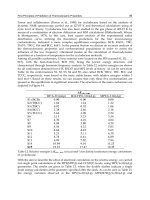
Fig. 9. Two sections of the surfaces
2
( Δ )
eo o
Κδ, α and
22
( Δ
oo o
|r δ , α )| shown in Fig. 8 when (a)
ΔΔ
max
oo
αα≡≈ 2.1 or (b)
22
max
δδ≡≈ 0.078;
0
λ
= 0.85 μm and
max
eo
Κ ≈ 10.8
Electromagnetic Waves in Crystals with Metallized Boundaries
63
Figure 9a (curve 1) shows that the section of the peak for ΔΔ
max
oo
αα= rapidly reaches a
maximum and then slowly decreases as the parameter
δ
increases. Of course, this is
advantageous for applications but restricts (at least, in the visible range) the applicability of
the approximation based on the inequality
δ
2
<< 1. The half-width of this peak is
22 0
1/2
ˆ
(Δ )42 82
max o e
δδζ/ κ n
′
== . (112)
Away from the section ΔΔ
max
oo
αα= , the coordinate of the maximum and the half-width of
the peak with respect to
δ
noticeably increase, which is clearly shown in the three-
dimensional picture of the peak in Fig. 8.
Another section of the same peak (for
22
max
δδ= ) is shown in Fig. 9b (curve 1). According to
(111)
2
, its half-width is
max
1/2
88||
() | |
||
oo
o
ζ
ζζ
αα
ζ
κ
γ
′
′′′
Δ=Δ=
′′
. (113)
Compared with (112), this quantity contains an additional small parameter |
ζ
′′
|, which
accounts for the relatively small width in this section of the peak in the region
|Δ |1
o
α << .
The penetration depth d
e
of a polariton into a crystal is limited by the parameter p
e
and,
according to (95), depends on the angle Δ
o
α . At the maximum point ΔΔ
max
oo
αα= (105), the
penetration depth is
02
0
0
0
ˆ
()
11
ˆ
Im 2 | |
Im
e
e
eoe
ee
n
d
kp
kn p
λ
π
εε ζ
=≈ =
′
′
. (114)
The plasmon penetration depth into the metal is found quite similarly
0
||
1
Im 2
m
m
d
kp
λ
ζ
π
′
′
=≈, (115)
where we have made use of Eq. (11)
4
by expressing Imp
m
≈
0
ˆ
1/| |
e
n
ζ
′
′
. Comparing Eqs. (114)
and (115), we can see that the plasmon in metal is localized much stronger than the
polariton in the crystal: d
m
/d
e
~
2
||
ζ
′
′
.
In Fig. 9, the material characteristics of the crystal
ε
o
and
ε
e
, as well as the geometric
parameters c
1
and c
2
are "hidden" in the normalizing factors
2
max
δ
,
Δ
max
o
α
, and
max
eo
Κ
. The first
section (Fig. 9a) is independent of other parameters and represents a universal characteristic
in a wide range of wavelengths, whereas the second section (Fig. 9b) depends on the ratio
/| |
ζ
ζ
′′′
obtained from Table 1 for aluminum at a vacuum wavelength of
λ
0
= 0.85 μm.
λ
0
, μm
0.4 0.5 0.6 0.85 1.2 2.5 5.0
ζ
′
0.0229 0.0234 0.0253 0.0373 0.0092 0.0060 0.0046
-
ζ
′′
0.267 0.215 0.180 0.135 0.108 0.050 0.026
Table 1. Components of the surface impedance i
ζζ ζ
′
′′
=
+ for aluminum in the visible and
infrared ranges at room temperature, obtained from the data of (Motulevich, 1969)
Wave Propagation
64
The absolute values of the main parameters of the peak are shown in Table 2 for a sodium
nitrate crystal NaNO
3
for various wavelengths. In our calculations (including those related
to Fig. 8), we neglected a not too essential dispersion of permittivities and used fixed values
of
ε
o
= 2.515,
ε
e
= 1.785, and
γ
= 0.711 (Sirotin & Shaskolskaya, 1979, 1982) at
λ
0
= 0.589 μm.
First of all, it is worth noting that, in the visible range of wavelengths of
λ
0
= 0.4 0.6 μm, the
maximal excitation factor (110) relatively slowly decreases as
λ
0
increases, although remains
rather large (
max
eo
Κ ≈ 16 18). With a further increase in the wavelength to the infrared region
of the spectrum, the factor first continues to decrease down to a point of
λ
0
= 0.85 μm and
then rather rapidly increases and reaches a value of about 90 at
λ
0
= 5 μm. The half-width of
the peak
1/2
)(Δ
o
α (113), starting from the value of
1/2
)(Δ
o
α ≈ 5°, rapidly decreases as the
wavelength increases and becomes as small as about 0.1° at
λ
0
= 5 μm, which, however, is
greater than the usual angular widths of laser beams. The half- width
1/2
2
)(Δδ
(112) differs
from
2
max
δ (107) only by a numerical factor of 24 and therefore is not presented in the
table. The penetration depth d
e
(114) of a polariton into the crystal at the point of absolute
maximum of the resonance peak is comparable with the wavelength of the polariton and
remains small even in the infrared region, although being much greater than the localization
depth d
m
of the plasmon (115). However, as
o
αΔ → 0, p
e
→ 0 (95), the penetration depth d
e
rapidly increases, and the polariton becomes a quasibulk wave. The optimized perturbation
δ
max
corresponding to the angle
θ
max
= arctan
δ
max
remains small over the entire range of
wavelengths and varies from 0.05 to 0.01, which certainly guarantees the correctness of the
approximate formulas obtained.
0
λ
,
μm
0.4 0.6 0.85 1.2 2.5 5.0
max
eo
K
17.6 15.9 10.8 43.8 67.1 87.5
1/2
(Δ )
o
α
5.5° 4.1° 4.5° 0.9° 0.3° 0.11°
e
d , μm
0.090 0.225 0.399 0.719 3.18 12.4
Δ
max
o
α−
8.0° 3.6° 2.1° 1.3° 0.3° 0.08°
2
max
δ 0.048 0.053 0.078 0.019 0.013 0.010
max
θ
12° 13° 16° 7.8° 6.5° 5.7°
Surface
polariton
(a pumped
mode)
Δ 0
max
o
α <
o
ψ
15° 15° 18° 9.3° 7.7° 6.8°
max
eo
K
2.7 3.9 4.6 6.9 14.4 26.3
2
max
δ
0.56 0.38 0.28 0.23 0.11 0.05
Bulk polariton
Δ 0
max
o
α =
max
θ
37° 32° 28° 26° 18° 13°
Plasmon
m
d ,
μm
0.017 0.017 0.018 0.021 0.020 0.021
Table 2. Parameters of polaritons excited in an optically negative sodium nitrate crystal with
aluminum coating for various wavelengths (c
1
= 0,
ˆ
o
α = 32.5°)
Electromagnetic Waves in Crystals with Metallized Boundaries
65
5.4. Conversion reflection and a pumped surface mode
Now we consider the reflection coefficient (97) in more detail for
Δ
o
α
< 0:
(
)
()
20
2
20
ˆ
/2 Δ
( Δ )
ˆ
/2 Δ
r
oe o o
o
oo o
i
o
oe o o
δκn ζ i κγ α |ζ |
C
r δ , α
C
δκn ζ i κγ α |ζ |
′
′′
−− − −
≡=
′
′′
++ − −
. (116)
In contrast to the excitation factor K
eo
(104) of the extraordinary polariton, the reflection
coefficient (116) does not "promise" any amplification peaks. Conversely, it follows from
(116) that the amplitude of the ordinary reflected wave never exceeds in absolute value the
amplitude of the incident wave. Moreover, the substitution of the coordinates Δ
max
o
α (105)
and
δ
max
(107) of the absolute maximum of the excitation factor (104) into (116) gives the
absolute minimum (see Fig. 8 and curves 2 in Fig. 9):
22
( Δ )0
max
oo max o
|r δ , α |
=
(117)
Thus, the resonance reflection in the optimized geometry is a conversion reflection (i.e., a
two-partial reflection with a change of branch) and a quite nontrivial one at that. Indeed, in
this case the incident ordinary partial wave in the crystal is accompanied by a unique wave,
which, being an extraordinary wave belongs to the other refraction sheet and is not a bulk
reflected wave. This wave is localized at the interface between the crystal and metal and
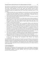
transfers energy along the interface (Fig. 10).
Fig. 10. Schematic picture of the pumped polariton-plasmon near the interface between a
crystal and metal coating
Naturally, in this case the absence of the reflected wave does not imply the violation of the
energy conservation law; just the propagation geometry corresponding to the minimum
(117) is chosen so that the normal component of the Poynting vector of the incident wave is
completely absorbed in the metal. This component is estimated by means of (100)
1
:
00 00
ˆˆˆ ˆ ˆˆ
sin ( / ) ( / ) /
ii i i
ooooooeo ooeo
||||α wc npn n cwpn ε
⊥
== =PP . (118)
Following (Landau & Lifshitz, 1993) and relations (100), (101), and (103), we can easily verify
that this component is equal the normal energy flux absorbed by the metal coating at
resonance:
Wave Propagation
66
00
22
ˆˆ
8
ii
oe
mtSeomaxoo
o
p
n
cζ
|| ||сζ |r | w cw
π
ε
⊥
′
′
== =
PH . (119)
It is not incidental that the final expression for
m
||
⊥
P does not contain the components of
the impedance. Indeed, according to the energy conservation law, in this case dissipation
should completely compensate the normal energy flux in the incident wave, which "knows"
nothing about the metallization of the crystal surface. It is essential that the dissipation (119),
remaining comparable with the energy flux density in the incident wave, is very small
compared with the intensity of the polariton plasmon localized at the interface:
22
000
1
ˆˆˆ
8
i
o
emax eS eS eomax m
eee
cw
cc
|| w| | | |r| | |
π
nnn
⊥
== = >>PH P. (120)
The fact that the energy flux of the polariton plasmon at the interface is considerably
greater than the intensity of the pumping wave in no way contradicts either the energy
conservation law or the common sense. We consider a steady-state problem on the
propagation of infinitely long plane waves. In this statement, the superposition of waves
jointly transfers energy along the surface from ∞ to +∞. These waves exist only together,
and the question of the redistribution of energy between the partial waves can be solved
only within a non-stationary approach. Indeed, suppose that, starting from a certain instant,
a plane wave coinciding with our ordinary wave is incident on the surface of a crystal. Upon
reaching the boundary, this wave generates an extraordinary wave whose amplitude
increases in time and gradually reaches a steady-state regime that we describe. Naturally,
the time of reaching this regime is the larger, the higher the peak of the excitation factor.
In fact, the conversion reflection considered represents an eigenwave mode that arises due
to the anisotropy of the crystal. It is natural to call this mode, consisting of a surface
polariton plasmon and a weak pumping bulk wave, a pumped surface wave by analogy
with the known leaky surface waves, which are known in optics and acoustics (Alshits et al.,
1999, 2001). The latter waves also consist of a surface wave and the accompanying weak
bulk wave, which, in contrast to our case, removes energy from the surface to infinity, rather
than brings it to the surface; i.e., it is a leak, rather than a pump, partial wave.
Numerical analysis of the exact expression for the reflection coefficient r
oo
, Eqs. (30)
1
, (32),
has shown (Lyubimov et al., 2010) that the conversion phenomenon (117) retains
independently of the magnitude of the impedance
ζ
. However it turns out that for not too
small
ζ
, positions of the maximum of the excitation factor K
eo
and the minimum (117) of the
reflection coefficient r
oo
do not exactly coincide anymore, as they do in our approximation.
5.5. Resonance excitation of a bulk polariton
When a pump wave of the ordinary branch is incident at angle
oo
αα
ˆ
≥ on the boundary of
the crystal, a bulk extraordinary polariton is generated. The expression, following from (96)
and (102), for the excitation factor K
eo
of such a polariton is significantly different from
expression (104), which is valid for 0Δ <
о
α :
()
20
2
2
20 2
ˆˆ
()
Δ
ˆ
Δ
oe o e
eo o
oe o o
δκ ε /nn
K(δ , α )
δκn/2 κγ α ζ ζ
=
′
′′
+++
. (121)
Electromagnetic Waves in Crystals with Metallized Boundaries
67
As the angle Δ
o
α increases, the function (121) monotonically decreases, so that the excitation
factor attains its maximum for
Δ 0
о
α
=
, i.e., for
ˆ
oo
αα
=
:
()
=
′
′′
++
20
2
2
20 2
ˆˆ
()
(0)
ˆ
ooe
eo
oe
e
δκ ε /nn
K δ ,
δκn/2ζζ
. (122)
In turn, formula (122), as a function of the parameter
2
δ , forms a peak with the coordinate
of the maximum
2
00
22
ˆˆ
max
oe oe
|ζ||ζ |
δ
κ n κ n
′
′
=≈ . (123)
Note that the optimized parameters
2
max
δ (123) and
2
max
δ (107) for the excitation of bulk and
localized polaritons are substantially different (see Table 1):
22
max max
δ / δ |ζ |/ζ
′
′′
≈
. (124)
With regard to (123), the absolute maximum of the excitation factor (121) is expressed as
()()
00
2
ˆˆ
22
(0)
ˆˆ
max
oo
eo eo max
oo
pp
KKδ ,
n|ζ| ζ n|ζ | ζ
== ≈
′
′′ ′
++
. (125)
Next, by analogy with (110) and with regard to (109), for c
1
= 0 we obtain the following
optimized value:
2
max
oe
eo
oe
εε
K
|ζ | ζεε
−
≈
′′ ′
+
. (126)
The approximate equality in formulas (123) (126) implies that the terms of order
2
~( / ) 1ζζ
′′′
<< are omitted.
The three-dimensional picture of the excitation peak (121) is shown in Fig. 8 as a slope of a
ridge in the region 0Δ ≥
о
α . The figure shows that, in the domain
max
δ~δ
,
о
αΔ ≈ 0, the
factor K
eo
(
δ
2
α, Δ
o
) rather weakly depends on δ and can be estimated at
max
δδ =
as
2
( Δ )
1 ΔΔ
max
eo
eo max o
max
oo
K
K δ , α
α /| α |
≈
+
. (127)
The half-width of this one-sided peak is obviously given by
|α|α
max
oo
Δ)(Δ
1/2
= . In Fig. 8,
the section (127) is shown as the edge of the surface K
eo
(
δ
2
α, Δ
o
) that reaches the plane
0.28
22
≈=
max
δδ
(see Table 2).
Note that, in the domain
Δ 0
о
α ≥ , conversion is impossible (r
oo
≠ 0) for
ζ
≠ 0; thus, along with
the extraordinary reflected wave, an ordinary reflected wave always exists, such that
22
1 Δ / Δ /
( Δ )
1 Δ / Δ /
max
oo
oo max o
max
oo
α | α | ζ |ζ |
|r δ , α |
α | α | ζ |ζ |
′
′′
−−
≈
′
′′
++
. (128)
Wave Propagation
68
where, just as in (127), the terms quadratic in
ζ
′
and linear in
Δ
o
α
are omitted. Formula
(128) shows that, for ΔΔ
max
oo
α | α |<< , ζ |ζ |
′
′′
<
< , the absolute values of the amplitudes of the
incident and ordinary reflected waves are rather close to each other; hence, if we neglect the
dissipation in the metal, nearly all the energy of the incident wave is passed to the ordinary
reflected wave. In this situation, the presence of additional quite intense extraordinary
reflected wave looks paradoxical.
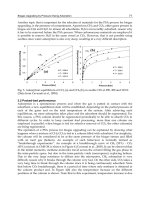
This result can be more clearly interpreted in terms of wave beams rather than plane waves
(Fig. 11). Let us take into consideration that plane waves are an idealization of rather wide
(compared to the wavelength) beams of small divergence. Of course, it is senseless to choose
the angle
Δ
o
α smaller than the angle of natural divergence of a beam. However, this angle
can be very small (10
-4
10
-3
rad) for laser beams. If the width of an incident beam of an
ordinary wave is l, then the reflected beam of the same branch of polarization has the same
width. However, the beam of an extraordinary wave is reflected at a small angle
e
ϕ
to the
surface, and its width
l
should also be small: /sin
eo
llα
ϕ
=
(Fig. 11). It can easily be shown
that this width decreases so that even a small amount of energy in a narrow beam ensures a
high intensity of this wave. The consideration would be quite similar to our analysis of the
energy balance in the previous sub-section.
Fig. 11. The scheme of the resonance excitation of a bulk polariton by a finite-width beam
Fortunately, even a small deviation of αΔ
o
from zero easily provides a compromise that
allows one, at the expense of the maximum possible intensity in the extraordinary reflected
wave, to keep this intensity high enough and, moreover, to direct a significant part of the
energy of the incident wave to this reflected wave. Indeed, formulas (127) and (128) show
that, say, at
|α|α
max
oo
Δ0.1Δ ≈
, the energy is roughly halved between the reflected waves,
and K
eo
≈ 0.76
max
eo
K
. For
|α|α
max
oo
Δ0.2Δ ≈
, we obtain |r
oo
|
2
≈ 0.3 and K
eo
≈ 0.7
max
eo
K
.
The ratio of the absolute maxima (110) and (126) taken for different optimizing parameters
2
max
δ and
2
max
δ , respectively, is usually much greater than unity:
2
2
( Δ )
1
1
2
(0)
max max
eo max o eo
max
eo max eo
K δ , α K
|ζ |
ζ
K δ ,K
′′
⎛⎞
=
=+
⎜⎟
′
⎝⎠
. (129)
In other words, the excitation efficiency of bulk polaritons is less than that of surface
polaritons (see Table 2). Nevertheless, the attainable values of the excitation factor
max
eo
K of a
bulk polariton are in no way small. According to Table 2, when Δα
o
= 0, the intensity of the
l
o
α
l
e
φ
o
αl/sin
o
e
l
l
α
ˆ
sin
φ
=
Electromagnetic Waves in Crystals with Metallized Boundaries
69
reflected extraordinary wave is three or four times greater than that of the incident ordinary
wave even in the visible range of wavelengths of 0.4 0.6 μm (however, since the parameter
2
max
δ in this part of the table is not small enough, the accuracy of these estimates is low).
Toward the infrared region, the surface impedance
ζ of the aluminum coating decreases
(see Table 1), while the excitation constant sharply increases, reaching values of tens.
5.6 Anormalous reflection of an extraordinary wave
Now we touch upon the specific features of the resonance excitation of an ordinary
polariton by an incident extraordinary pumping wave. As mentioned above, such an
excitation is possible only in optically positive crystals (
γ
> 1). The resonance arises under
the perturbation of the geometry in which a bulk polariton of the ordinary branch (54) and
simple reflection (44)-(46) in the extraordinary branch exist independently of each other.
Let us slightly "perturb" the orientation of the crystal surface by rotating it through a small
angle
2
arcsincθ
= with respect to the optical axis: c = (c
1
, ,c
2
c
3
). The structure of the
corresponding perturbed wave field is determined by formula (5) at 0=
i
o
C in which the
appropriate vector amplitudes (6), (7) are substituted. The perturbed polarization vectors
are found from formulas (14), (15), and the geometrical meaning of the parameters p, p
e
, and
p
o
is illustrated in Fig. 2a. The refraction vectors, which determine the propagation direction
of the incident and reflected waves, are present in (10). In the considered case the horizontal
component n of the refraction vector is close to the limiting parameter
oo
εn =
ˆ
(Fig. 3), and
the parameter p
e
is close to the limiting value of
e
p
ˆ
: n =
o
n
ˆ
+ Δn,
eee
ppp Δ+=
ˆ
. Here the
parameter
e
p
ˆ
is given by the exact expression
22
1
2
)1)(( /AcAγp
e
−−=
ˆ
and p is defined by
Eq. (11) as before. The angle of incidence
e
α of the extraordinary wave ( Fig. 2a) is now close
to the angle )arctan( ppα
ee
−=
ˆˆ
:
eee
ααα Δ+=
ˆ
. The relation between the increments Δn,
e
pΔ ,
and
e
αΔ has the form
02 2
13
ˆ
Δ ()Δ
eo e
npnc/γ c α=− + ,
22
13
Δ ()Δ
ee
pcγc α=+ , (130)
where
0
ˆ
e
p
relates to the unperturbed c
2
= 0 :
0
3
ˆ
|| 1
e
pc γ
=
−
. Another important
characteristic of the resonance is the angle of reflection
β
o
,
β
o
= arctanp
o
,
ΔΔ0,
ΔΔ0,
ee
ooe
ee
α , α
p εκ
i α , α
⎧
≥
⎪
≈
⎨
−<
⎪
⎩
(131)
02 2
13
ˆ
2(/ /)
ee e o
κ pc ε c ε=+
. (132)
Introduce a small parameter
23
/δ cc=
, which is the inverse of (98)
2
. Now, instead of (96)
and (97), we have the following expressions for the reflection coefficients:
0
20
ˆ
2
( Δ )
ˆˆ
Δ
r
ee
o
oe e
i
eeoee
p δ / ε
C
r δ, α
C δ p/n κα ζ
≡=
+
+
, (133)
20
2
20
ˆˆ
Δ
( Δ )
ˆˆ
Δ
r
eo ee
e
ee e
i
eeoee
δ p/n κα ζ
C
r δ , α
C δ p/n κα ζ
−
−
≡=
+
+
. (134)
Wave Propagation
70
These expressions exhibit the same structure of dependence on the small parameters
δ
and
Δ
e
α as formulas (96) and (97) for optically negative crystals. Naturally, the main features of
the reflection resonance considered above nearly completely persist under new conditions.
By analogy with (99), let us introduce the excitation factor of an ordinary polariton,
2
2
0
( Δ )/ (||/||)(Δ )
ri r i
eoe o o e
y
oe oe
K δ , α r δ, α
=
==PP u u , (135)
where
r
o
u
and
i
e
u
are the group velocities (3) of the excited and incident waves (in zero
approximation):
ˆ
|| /
r
oo
cn=u
,
ˆ
|| /
i
o
e
cB n=u
.
The analysis of expressions (133) (135) shows that, when
20
ˆˆ
max o e
δ n ζ /p
′
= ,
2
Δ
max
ee
α |ζ |/κ
′′
=− , (136)
a conversion occurs (r
ee
= 0); i.e., the amplitude of the extraordinary reflected wave strictly
vanishes. As a result, again a pumped polariton plasmon arises in which the primary mode
is the localized mode (an ordinary polariton in the crystal and a plasmon in the metal)
whose intensity on the interface is much greater than the intensity of the incident pumping
wave, which is clear from the expression for the absolute maximum of the excitation factor:
(
)
20
ˆˆ
Δ
max max
oe max e oe e o e
K δ , α Kpn/εζ B
′
≡= . (137)
Substituting here
0
3
ˆ
1
e
p|c|γ
=
− , we can easily see that again the factor
max
oe
K is optimized
for c
1
= 0 when c
3
≈ 1. In this case,
1
max
eo
eo
oe
εε
K
ζεε
−
=
′
. (138)
Formulas (138) and (126) turn into each other under the interchange e ↔ o.
The penetration depth of the polariton into the crystal in the pumped configuration is
0
/2
oo
d
λ
πε |ζ |
′
′
=
. (139)
In the neighborhood of coordinates (136) of the absolute maximum (137), a peak of the
excitation factor K
oe
(
2
δ , αΔ
e
) is formed whose configuration is qualitatively correctly
illustrated in Figs. 8 and 9. The half-widths of the curves that arise in two sections of this
peak
max
ee
αα ΔΔ ≡ and
22
max
δδ ≡ are, respectively, given by
20
1/2
ˆˆ
(Δ )42
oe
δ n ζ /p
′
= ,
1/2
(Δ )8 /
ee
αζ|ζ | κ
′
′′
=
. (140)
The excitation resonance of a bulk polariton in the crystal for αΔ
e
≥0 is also completely
analogous to the resonance described above. Again the excitation factor is the larger, the
smaller is the deviation angle αΔ
e
, and again a peak arises with respect to
δ
2
:
202
2
20 2 2
ˆ
4()/
(,0)
ˆˆ
()
ee
oe
eo
δ p ε B
K δ
δ p/n ζζ
=
′
′′
++
, (141)
Electromagnetic Waves in Crystals with Metallized Boundaries
71
the coordinate of whose maximum is given by
200
ˆˆˆ ˆ
//
max o e o e
δ n|ζ|p n|ζ |p
′′
=≈ , (142)
and the peak height (the absolute maximum) is given by an analog of (125):
20
ˆˆ
0/()
max
oe oe max o e e
KK(δ ,) 2np ε B|ζ | ζ
′
′′
=
≈+. (143)
As above, the choice of the geometry c
1
= 0 optimizes the factor
max
eo
K and reduces (143) to
the following analog of (126):
2
max
eo
eo
oe
εε
K
|ζ | ζεε
−
=
′′ ′
+
. (144)
The maximum intensity (143), (144) of the bulk wave attained for
Δ
e
α = 0 is again
accompanied by zero integral energy in this wave, because the main part of the incident
extraordinary wave (except for the absorption in metal) is transferred to a reflected
extraordinary wave. However, as is shown in Subsection 5.5, even a small increase in the
angle of incidence from the value
Δ
e
α = 0 substantially improves the energy distribution
between reflected waves with a small loss in the amplitude of the excitation factor. This fact
can easily be verified quantitatively by analyzing formulas (127) and (128) upon the
interchange of the indices o ↔ e.
6. Recommendations for setting up an experiment
The resonance discussed is completely attributed to the anisotropy of the crystal and the
shielding of the wave field in the crystal by metallization of the surface. Therefore, one
should choose a crystal with large anisotropy factor | γ 1| and a metal with low surface
impedance
ζ . This will guarantee the maximum intensity of the wave excited during
reflection (see formulas (112), (140) and (128), (145)).
The orientation of the working surfaces of a sample is determined by the optical sign and
the permittivities of the crystal and by the impedance of the metal coating at a given
wavelength. As shown above, the optical axis should be chosen to be orthogonal to the
propagation direction x: c
1
= 0 (Fig. 1). In optically positive and negative crystals, this axis
should make angles of
θ
max
and 90°
θ
max
, respectively, with the metallized surface. When a
surface polariton plasmon is excited in an optically positive crystal, we have
arctan
max max
θδ= ,
2
o
max
eo
ζε
δ
εε
′
=
−
. (145)
If the goal of the experiment is to obtain an intense bulk reflected wave, then one should
change
2
max
δ to
22
max max
δδζ|/ζ
′
′′
= (i.e.,
ζ |ζ |
′
′′
→
) and
θ
max
to
max
θ in (145). For optically
negative crystals, appropriate angles
θ
max
and
max
θ are defined by the same formulas (145) in
which the indices o and e should be interchanged. For sodium nitrate crystals, the angles
θ
max
and
max
θ are given in Table 2.
In an optically positive crystal in which a surface polariton plasmon is excited, the input
surface for a normally incident initial wave should be cut at the angle
Wave Propagation
72
ˆ
Δ
max
ee e
αα α=+ ,
2
2
( 1)(1 )
ˆ
arctan
1
max
e
max
γδ
α
γδ
−+
=
+
,
2
Δ
21
max
o
e
|ζ | ε
α
γ
′′
=−
−
. (146)
In the case of excitation of a bulk polariton, one should make the following changes in (146):
ˆ
e
α →
ˆ
e
α and
2
max
δ →
2
max
δ . The expressions for
ˆ
e
α and
ˆ
e
α following from (146) are exact.
We did not decompose them with respect to the parameters
2
max
δ and
2
max
δ , because they are
not small enough at some wavelengths. To successfully observe a resonance, one should
determine the angles of incidence as precisely as possible, especially when the angular
width of the resonance is small.
In an optically negative crystal, instead of (146) we have
ˆ
Δ
max
oo o
αα α=+ ,
ˆ
arctan 1 1
o
α / γ
=
− ,
2
Δ
21 1
max
o
o
|ζ | ε
α
/ γ
′′
=−
−
. (147)
Here the limiting angle
ˆ
o
α
is insensitive to the perturbation of c
3
, being the same for the
excitation of localized and bulk polaritons (see Table 2).
The output surface for the excited bulk wave should be orthogonal to its refraction vector,
determined in an optically positive or negative crystal by the angle
β
o
or
β
e
(Figs. 2a and 7b):
(
)
arctan
oo
β
|ζ | ε
′′
= ,
(
)
arctan
ee
β
|ζ | ε / γ
′′
= . (148)
For optically negative crystals, the angle
β
e
is naturally different from the slope angle
φ
e
of its
ray velocity
u
e
in the reflected beam (see Figs. 7b and 11).
A correct choice of the polarization of the incident laser beam allows one to avoid the
occurrence of a parasitic beam as a result of birefringence at the input of the crystal, i.e.,
additional loss of the energy of the incident beam. According to (45) and (50) for c
1
= 0, the
polarization of the wave at the input should be of TE type in zero approximation
δ
= 0): the
field
e
i
is parallel to the z axis for crystals of both optical signs. In a more precise analysis
(
δ
=
δ
max
), the polarization vector e
i
should be turned (about the vector n
i
) through an angle
ψ
. When exciting a surface polariton plasmon, in the first approximation this angle is given
by
arctan( / )
max
ψδγ≈
; (149)
in optically negative crystals, this rotation is clockwise, whereas, in optically positive
crystals, counterclockwise. Table 2 shows that the angle
ψ
is small.
The situation is changed when one deals with the excitation of a bulk wave. Now the
optimized polarization of the incident wave is defined by the same Eq. (149) in which
δ
max
is
replaced by
max
δ . In this case, the rotation angle
ψ
sharply increases, while the accuracy of
approximation substantially degrades (at least for the visible range). It seems that in this
case it is better to choose an optimal polarization of the initial wave experimentally.
As we have seen, the resonance width with respect to the angle of incidence sharply
decreases when passing to the infrared region to values of ( αΔ
o,e
)
1/2
≈ 0.1. This imposes a
constraint on the divergence of the initial laser beam: the higher the divergence of a beam,
the larger part of this beam goes out of resonance. One should also take into account that, by
narrowing down the beam at the input, we increase its natural diffraction divergence.
Electromagnetic Waves in Crystals with Metallized Boundaries
73
7. Acknowledgements
This work was supported by the Polish Foundation MNiSW, project no. NN501252334. One
of the authors (V.I.A.) acknowledges the support of the Polish Japanese Institute of
Information Technology, Warsaw, and the Kielce University of Technology, Poland.
8. References
Agranovich, V.M. (1975). Crystal optics of surface polaritons and the properties of surfaces.
Usp. Fiz. Nauk, Vol. 115, No. 2 (Feb., 1975) 199-237, ISSN 0042-1294 [Sov. Phys. Usp.,
Vol. 18, No. 2, (1975) 99-117, ISSN 1063-7859]
Agranovich, V.M. & Mills, D.L. (Eds.) (1982). Surface Polaritons: Electromagnetic Waves at
Surfaces and Interfaces, North-Holland, ISBN 0444861653, Amsterdam
Alshits, V.I.; Gorkunova, A.S.; Lyubimov, V.N.; Gierulski, W.; Radowicz, A. & Kotowski,
R.K. (1999). Methods of resonant excitation of surface waves in crystals, In: Trends
in Continuum Physics (TRECOP ’88), B.T. Maruszewski, W. Muschik & A. Radowicz,
(Eds.), pp. 28-34, World Scientific, ISBN 981023760X, Singapore.
Alshits, V.I. & Lyubimov, V.N. (2002a). Dispersionless surface polaritons in the vicinity of
different sections of optically uniaxial crystals. Fiz. Tverd. Tela (St. Petersburg), Vol.
44, No. 2 (Feb., 2002) 371-374, ISSN 0367-3294 [Phys. Solid State, Vol. 44, No. 2 (2002)
386-390, ISSN 1063-7834]
Alshits, V.I. & Lyubimov, V.N. (2002b). Dispersionless polaritons on symmetrically oriented
surfaces of biaxial crystals. Fiz. Tverd. Tela (St. Petersburg), Vol. 44, No. 10 (Oct.,
2002) 1895-1899, ISSN 0367-3294 [Phys. Solid State, Vol. 44, No. 10 (2002) 1988-1992,
ISSN 1063-7834]
Alshits, V.I. & Lyubimov, V.N. (2005). Dispersion polaritons on metallized surfaces of
optically uniaxial crystals. Zh. Eksp. Teor. Fiz., Vol. 128, No. 5 (May, 2005) 904-912,
ISSN 0044-4510 [JETP, Vol. 101, No. 5 (2005) 779-787, ISSN 1063-7761]
Alshits, V.I. & Lyubimov, V.N. (2009a). Generalization of the Leontovich approximation for
electromagnetic fields on a dielectric – metal interface. Usp. Fiz. Nauk, Vol. 179, No.
8, (Aug., 2009) 865-871, ISSN 0042-1294 [Physics – Uspekhi, Vol. 52, No.8 (2009) 815-
820, ISSN 1063-7859]
Alshits, V.I. & Lyubimov, V.N. (2009b). Bulk polaritons in a biaxial crystal at the interface
with a perfect metal. Kristallografiya, Vol. 54, No. 6 (Nov., 2009) 989-993, ISSN 0023-
4761 [Crystallography Reports, Vol. 54, No. 6 (2009) 941-945, ISSN 1063-7745]
Alshits, V.I.; Lyubimov, V.N. (2010). Resonance excitation of polaritons and plasmons at the
interface between a uniaxial crystal and a metal. Zh. Eksp. Teor. Fiz., Vol. 138, No. 4
(Oct., 2010) 669-686, ISSN 0044-4510 [JETP, Vol. 111, No. 4 (2010) 590-606, ISSN
1063-7761]
Alshits, V.I.; Lyubimov, V.N. & Radowicz, A. (2007). Electromagnetic waves in uniaxial
crystals with metallized boundaries: mode conversion, simple reflections, and bulk
polaritons. Zh. Eksp. Teor. Fiz., Vol. 131, No. 1 (Jan., 2007) 14-29, ISSN 0044-4510
[JETP, Vol. 104, No. 1 (2007) 9-23, ISSN 1063-7761]
Alshits, V.I. ; Lyubimov, V.N. & Shuvalov, L.A. (2001). Pseudosurface dispersion polaritons
and their resonance excitation. Fiz. Tverd. Tela (St. Petersburg), Vol. 43, No. 7 (Jul.,
2001) 1322-1326, ISSN 0367-3294 [Phys. Solid State, Vol. 43, No. 7 (2001) 1377-1381,
ISSN 1063-7834]
Wave Propagation
74
Born, M. & Wolf, E. (1986). Principles of Optics, Pergamon press, ISBN 0.08-026482.4, Oxford
Depine, R.A. & Gigli, M.L. (1995). Excitation of surface plasmons and total absorption of
light at the flat boundary between a metal and a uniaxial crystal. Optics Letters, Vol.
20, No. 21 (Nov., 1995) 2243-2245, ISSN 0146-9592
D’yakonov, M.I. (1988). New type of electromagnetic wave propagating at the interface. Zh.
Eksp. Teor. Fiz., Vol. 94, No. 4 (Apr., 1988) 119-123, ISSN 0044-4510 [Sov. Phys. JETP,
Vol. 67, No. 4 (1988) 714-716, ISSN 1063-7761]
Fedorov, F.I. (2004). Optics of Anisotropic Media (in Russian), Editorial URSS, ISBN 5-354-
00432-2, Moscow
Fedorov, F.I. & Filippov, V.V. (1976). Reflection and Refraction of Light by Transparent Crystals
(in Russian), Nauka I Tekhnika, Minsk
Furs, A.N. & Barkovsky, L.M. (1999). General existence conditions for polaritons in
anisotropic, superconductive and isotropic systems J. Opt. A: Pure Appl. Opt., Vol. 1
(Jan., 1999) 109-115, ISSN 1464-4258
Landau, L.D. & Lifshitz, E.M. (1993) Electrodynamics of Continuous Media, Butterworth-
Heinemann, ISBN, Oxford
Lyubimov, V.N.; Alshits, V.I.; Golovina, T.G.; Konstantinova, A.F. & Evdischenko, E.A.
(2010). Resonance and conversion reflections from the interface between a crystal
and a metal. Kristallografiya, Vol. 55, No. 6 (Nov., 2010) 968-974, ISSN 0023-4761
[Crystallography Reports, Vol. 55, No. 6 (2010) 910-916 ISSN 1063-7745]
Marchevskii, F.N.; Strizhevskii, V.L. & Strizhevskii, S.V. (1984). Singular electromagnetic
waves in bounded anisotropic media Fiz. Tverd. Tela (St. Petersburg), Vol. 26, No. 5
(May, 1984) 1501-1503, ISSN 0367-3294 [Sov. Phys. Solid State, Vol. 26, No. 5 (1984)
911-913, ISSN 1063-7834]
Motulevich G.P. (1969). Optical properties of polyvalent non-transition metals. Usp. Fiz.
Nauk, Vol. 97, No. 2 (Jan., 1969) 211-256, ISSN 0042-1294 [Sov. Phys. Usp., Vol. 12,
North-Holland, No. 1, 80-104, ISSN 1063-7859]
Sirotin, Yu.I. & Shaskol’skaya, M.P. (1979). Fundamentals of Crystal Physics (in Russian),
Nauka, Moscow [(1982) translation into English, Mir, ISBN , Moscow]
4
Electromagnetic Waves Propagation
Characteristics in Superconducting
Photonic Crystals
Arafa H Aly
Physics department, Faculty of Sciences, Beni-suef University
Egypt
1. Introduction
Photonic crystals (PCs) are structures with periodically modulated dielectric constants
whose distribution follows a periodicity of the order of a fraction of the optical wavelength.
Since the first pioneering work in this field, many new interesting ideas have been
developed dealing with one-dimensional (1D), two-dimensional (2D), and three-
dimensional (3D) PCs. Researchers have proposed many new and unique applications of
photonic devices which may revolutionize the field of photonics in much the same way as
semiconductors revolutionized electronics. They can generate spectral regions named
photonic band gaps (PBGs) where light cannot propagate in a manner analogous to the
formation of electronic band gaps in semiconductors [1,2]. There are several studies of
metallic [3-7] and superconducting photonic crystals [7,8] which are mostly concentrated at
microwave, millimeterwave, and far-infrared frequencies. In those frequencies, metals act
like nearly perfect reflectors with no significant absorption problems.
Yablonovitch [1] main motivation was to engineer the photonic density of states in order to
control the spontaneous emission of materials embedded with photonic crystal while John’s
idea was to use photonic crystals to affect the localization and control of light. However due
to the difficulty of actually fabricating the structures at optical scales early studies were
either theoretical or in the microwave regime where photonic crystals can be built on the far
more reading accessible centimeter scale. This fact is due to the property of the
electromagnetic fields known as scale invariance in essence, the electromagnetic fields as the
solutions to Maxwell’s equations has no natural length scale and so solutions for centimeter
scale structure at microwave frequencies as the same for nanometer scale structures at
optical frequencies.
The optical analogue of light is the photonic crystals in which atoms or molecules are
replaced by macroscopic media with different dielectric constants and the periodic potential
is replaced by a periodic dielectric function. if the dielectric constants of the materials is
sufficiently different and also if the absorption of light by the material is minimal then the
refractions and reflections of light from all various interfaces can produce many of the same
phenomena for photons like that the atomic potential produced for electrons[9].
The previous details can guide us to the meaning of photonic crystals that can control the
propagation of light since it can simply defined as a dielectric media with a periodic
Wave Propagation
76
modulation of refractive index in which the dielectric constant varies periodically in a
specific directions. Also it can be constructed at least from two component materials with
different refractive index due to the dielectric contrast between the component materials of
the crystal .it’s characterized by the existence of photonic band gap (PBG) in which the
electromagnetic radiation is forbidden from the propagation through it.
Optical properties of low dimensional metallic structures have also been examined recently.
For example, the optical transmission through a nanoslit collection structure shaped on a
metal layer with thin film thickness was analyzed in Refs. [10,11]. The photonic band
structures of a square lattice array of metal or semiconductor cylinders, and of an array of
metal or semiconductor spheres, were enumerated numerically in Ref. [12]. In addition,
superconducting (SC) photonic crystals also attract much attention recently [13,14]. In new
experiments superconducting metals (in exact, Nb) have been used as components in optical
transmission nanomaterials. Dielectric losses are substantially reduced in the SC metals
relative to analogous structures made of normal metals. The dielectric losses of such a SC
nanomaterial are reduced by a factor of 6 upon penetrating into the SC state [15]. Indeed,
studies of the optical properties of superconductor metal/dielectric multilayers are not
numerous, may be the results have been used in the design of high reflection mirrors, beam
splitters, and bandpass filters [16]. The superiority of a photonic crystal with
superconducting particles is that the scattering of the incident electromagnetic wave due to
the imaginary part of the dielectric function is much less than for normal metallic particles at
frequencies smaller than the superconducting gap. The loss caused by a superconducting
photonic crystal is thus expected to be much less than that by a metallic photonic crystal. For
a one-dimensional superconductor–dielectric photonic crystal (SuperDPC), it is seen like in
an MDPC that there exists a low-frequency photonic band gap (PBG). This low frequency
gap is not seen in a usual DDPC. This low frequency PBG is found to be about one third of
the threshold frequency of a bulk superconducting material [12]. In this paper, based on the
transfer matrix method, two fluid models, we have investigated the effect of the different
parameters on transmittance and PBG in a one-dimensional superconductor-dielectric
photonic crystals.
2. Numerical methods
We will explain in brief a mathematical treatment with a simple one dimensional photonic
crystal structure (1DPC) (see fig.1) which is composed of two materials with thicknesses (
2
d
and
3
d ) and refractive indices (
2
n and
3
n ) respectively. The analysis of the incident
electromagnetic radiation on this structure will be performed using the transfer matrix
method (TMM).
A one-dimensional nonmagnetic conventional and high tempeature superconductor-
dielectric photonic crystal will be modelled as a periodic superconductor-dielectric
multilayer structure with a large number of periods N » 1, Such an N-period superlattice is
shown in Fig. 1, where
23
dd d
=
+ is the spatial periodicity, where
2
d is the thickness of the
superconducting layer and
3
d denotes the thickness of the dielectric layer. We consider that
the electromagnetic wave is incident from the top medium which is taken to be free space
with a refractive index,
1
n = 1. The index of refraction of the lossless dielectric is given by
3
n =
3r
ε
,
2
n the index of refraction of the superconductor material, which can be described
Electromagnetic Waves Propagation Characteristics in Superconducting Photonic Crystals
77
Fig. 1. A superconductor dielectric structure. The thicknesses of superconducting and
dielectric are denoted by d
2
and d
3
, respectively, and the corresponding refractive indices
are separately indicated by n
1
, n
2
n
3
, where n
1
=1 and n
4
is the indexof substrate layer.
on the basis of the conventional two- fluid model [18].Accordingly to the two fluid model
the electromagnetic response of a superconductor can be described in terms of the complex
conductivity,
σ
=
12
i
σ
σ
−
, where the real part indicating the loss contributed by normal
electrons, and the imaginary part is due to superelectrons, the imaginary part is expressed
as [19,20]
2
σ
=
2
0
1/
l
ω
μλ
, where the temperature-dependent penetration depth is given
by
0
() /1 ()
ll
TfT
λλ λ
== − , where Gorter-Casimir expression for ƒ (T) is given for low and
conventional superconductor by ƒ (T)=
()
4
/
c
TT , and for high temperature superconductor ƒ
(T)=
()
2
/
c
TT
[13,18].
We shall consider the lossless case, meaning that the real part of the complex conductivity of
the superconductor can be neglected and consequently it becomes
2
20
(1/ )
l
ii
σ
σωμλ
=− =− .
The relative permittivity as well as its associated index of refraction can be obtained by,
2
2
22
1
r
l
c
ε
ω
λ
=− and n
2
22
22
1
r
l
c
ε
ω
λ
==−
(1)
We will go to mention the mathematical form of the dynamical matrices and for the
propagation matrix to obtain an expressions for the reflection and transmission, the
dynamical matrices take the form [17]:-
1
1
D
nCos
nCos
α
αα
α
α
θ
θ
⎛
⎞
=
⎜
⎟
⎜
−
⎠
⎝
for S – wave (2)
Cos Cos
D
nn
α
α
α
αα
θ
θ
⎛⎞
=
⎜⎟
−
⎝⎠
for P – wave (3)
with
nSin
c
α
α
ω
β
θ
=
, and
x
knCos
c
α
αα
ω
θ
=
Wave Propagation
78
while the propagation matrix take the form:-
(
)
()
0
exp
exp
0
i
P
i
α
η
α
φ
φ
⎛⎞
=
⎜⎟
⎜⎟
−
⎝⎠
(4)
Since the number of the propagation matrix depend on the number of materials which build
our structure [17]. Finally the transfer matrix method can take the form:-
11 12
21 22
MM
M
MM
⎛⎞
=
⎜⎟
⎝⎠
(5)
11
2
11
0
0
Cos iSin
P
Cos iSin
φφ
φ
φ
+
⎛
⎞
=
⎜
⎟
⎜
−
⎠
⎝
22
3
22
0
0
Cos iSin
P
Cos iSin
φφ
φ
φ
⎞
+
⎛
=
⎟
⎜
⎟
−
⎝
⎠
Since;
2
122
2 d
nCos
π
φ
θ
λ
=
, and
3
233
2 d
nCos
π
φ
θ
λ
=
.
The components of the transfer matrix method can be written in a detailed form for an S –
wave as:-
()
()
44 3344
11 2 2 1
11 1133
2244 332424
2
1122 221313
2
1
1
2
1
2
n Cos n Cos n Cos
MCos iSinCos
n Cos n Cos n Cos
n Cos n Cos n Cos n n Cos Cos
Cos
n Cos n Cos n Cos n n Cos Cos
i
iSin
θθθ
φφφ
θθθ
θθ θ θθ
φ
θθ θ θθ
φ
⎡⎤
⎛⎞
⎛⎞
⎢⎥
⎜⎟
=+ + + +
⎜⎟
⎜⎟
⎢⎥
⎝⎠
⎝⎠
⎣⎦
⎡⎤
⎛⎞⎛ ⎞
+++
⎢⎥
⎜⎟⎜ ⎟
⎢⎥
⎝⎠⎝ ⎠
⎢⎥
⎣⎦
()
1
Sin
φ
(6)
()
()
44 3344
12 2 2 1
11 1133
2244 332424
2
1122 221313
2
1
1
2
1
2
n Cos n Cos n Cos
MCos iSinCos
n Cos n Cos n Cos
n Cos n Cos n Cos n n Cos Cos
Cos
n Cos n Cos n Cos n n Cos Cos
i
iSin
θθθ
φφφ
θθθ
θθ θ θθ
φ
θθ θ θθ
φ
⎡⎤
⎛⎞
⎛⎞
⎢⎥
⎜⎟
=− + − +
⎜⎟
⎜⎟
⎢⎥
⎝⎠
⎝⎠
⎣⎦
⎡⎤
⎛⎞⎛ ⎞
−+−
⎢⎥
⎜⎟⎜ ⎟
⎢⎥
⎝⎠⎝ ⎠
⎢⎥
⎣⎦
()
1
Sin
φ
(7)
()
()
44 3344
21 2 2 1
11 1133
2244 332424
2
1122 221313
2
1
1
2
1
2
n Cos n Cos n Cos
MCos iSinCos
n Cos n Cos n Cos
n Cos n Cos n Cos n n Cos Cos
Cos
n Cos n Cos n Cos n n Cos Cos
i
iSin
θθθ
φφφ
θθθ
θθ θ θθ
φ
θθ θ θθ
φ
⎡⎤
⎛⎞
⎛⎞
⎢⎥
⎜⎟
=− − − −
⎜⎟
⎜⎟
⎢⎥
⎝⎠
⎝⎠
⎣⎦
⎡⎤
⎛⎞⎛ ⎞
−−−
⎢⎥
⎜⎟⎜ ⎟
⎢⎥
⎝⎠⎝ ⎠
⎢⎥
⎣⎦
()
1
Sin
φ
(8)
Electromagnetic Waves Propagation Characteristics in Superconducting Photonic Crystals
79
()
()
44 3344
22 2 2 1
11 1133
2244 332424
2
1122 221313
2
1
1
2
1
2
n Cos n Cos n Cos
MCos iSinCos
n Cos n Cos n Cos
nCos nCos nCos nnCos Cos
Cos
nCos nCos nCos nnCos Cos
i
iSin
θθθ
φφφ
θθθ
θθ θ θθ
φ
θθ θ θθ
φ
⎡⎤
⎛⎞
⎛⎞
⎢⎥
⎜⎟
=+ − + −
⎜⎟
⎜⎟
⎢⎥
⎝⎠
⎝⎠
⎣⎦
⎡⎤
⎛⎞⎛ ⎞
+−+
⎢⎥
⎜⎟⎜ ⎟
⎢⎥
⎝⎠⎝ ⎠
⎢⎥
⎣⎦
()
1
Sin
φ
(9)
Where the reflectance and transmittance can be written as:-
2
2
21
11
M
Rr
M
== (10)
2
2
44 44
11 1111
1
nCos nCos
Tt
nCos nCos M
θθ
θθ
== (11)
Where r and t is the reflection and transmission and we can also obtain by the same method
the components of the transfer matrix method (TMM) for P– wave.
3. Results and discussions
The periodicity of the permittivity plays the same role for the photons that propagate inside
the structure than the atomic potential for the electrons. Leading further this analogy, the
thicknesses and the index contrast of the photonic crystal determinate many of its optical
properties as it does for conduction properties of semiconductors. Playing on these two
parameters, we can obtain frequency ranges for which light propagation is forbidden in the
material and others ranges for which light can propagate. These frequency ranges are also
scale dependent. Reducing the size of the elementary cell of the periodic lattice shifts the
whole frequency range to higher values. The consequence of this property is the possibility
to transpose a photonic crystal design from the microwave domain to infrared or visible
wavelengths. In our results we have studied one dimensional superconducting
(Super)/dielectric (Na3AIF6) photonic crystals (SuperDPC’s). In all our figures we have
used the thickness of Na3AIF6 layer is 320nm and the thickness layer of superconducting
material is 80nm. Also we have used different periods equal to 7 and the incidence of angle
is 48° for the all our results (Fig’s 2 and 3).
In fig. 2a we have examined the transmittance in the case of s-polarized depend on the
wavelengths in the range of ultraviolet (UV), visible (VI) and near infrared (NIR). We have
obtained the magnitude of transmittance 100% from 100nm to 350nm UV range) and we
have obtained the PBG from 600nm to 1050nm. At the 730 nm we have got unique peak
explaining as a defect localized mode which can be used as Fabry-Port micro cavity, this is a
good application. In the case of p-polarized (fig.2b), we can show different results and there
are about seven PBG's in the range from 100nm to 900nm. The width of each PBG is widest
at the long wavelength as from 700nm to 900nm and is narrowest at the short wavelengths
as at 100 nm. Also we have examined the angle dependence on wavelengths to
Super/Nas3AIF6 structure (fig.3).
Wave Propagation
80
0
20
40
60
80
100
100 200 300 400 500 600 700 800 900 1000 1100 1200
Transmittance (%)
(a) Wavelength (nm)
Super(80nm)/Na3AIF6(320nm),Theta=48,N=7
p-pol
0
20
40
60
80
100
100 200 300 400 500 600 700 800 900 1000 1100 1200
Transmittance (%)
(b) Wavelength (nm)
Super(80nm)/Na3AIF6(320nm),Theta=48,N=7
s-pol
Fig. 2. The transmittance spectra in Super (
80nm)/Na3AIF6 (329nm) structure, N=7,a) p-pol
and b)s-pol
Electromagnetic Waves Propagation Characteristics in Superconducting Photonic Crystals
81
100 89 78 67 56 44 33 22 11 0
Generated by an evaluation version of C1Chart2D
Generated by an evaluation version of C1Chart2D
Generated by an evaluation version of C1Chart2D
Generated by an evaluation version of C1Chart2D
Fig. 3. The incident angle dependence on wavelength to Super/ Na3AIF6 structure
4. Conclusion
We performed numerical analyses to investigate the wave propagation characteristics of a
simple-one dimensional superconducting(Super)-dielectric Na3AIF6 structure.The
advantage of a photonic crystal with superconducting particles is that the dissipation of the
incident electromagnetic wave due to the imaginary part of the dielectric function is much
greater for normal metallic than for superconducting particles, because the imaginary part
of the dielectric function for superconducting particles is negligible in comparison with the
imaginary part of the dielectric function for normal metal particles at frequencies smaller
than the superconducting gap. We have obtained good applications at the 730 nm and we
have got unique peak explaining as a defect localized mode which can be used as Fabry-Port
micro cavity.
5. References
[1] E. Yablonovitch, Phys. Rev. Lett. 58, 2059, (1987).
[2] S. John, Phys. Rev. Lett. 58,2487, (1987).
[3] A.R. McGurn, A.A. Maradudin, Phys. Rev. B 48 (1993) 17576
Wave Propagation
82
[4] M. M. Sigalas, C. T. Chan, K. M. Ho, and C. M. Soukoulis, Phys. Rev. B 52, 11 744 ,
(1995).
[5] J. S. McCalmont, M. M. Sigalas, G. Tuttle, K. M. Ho, and C. M. Soukoulis, Appl. Phys.
Lett. 68, 2759, (1995).
[6] Arafa H Aly and Sang-Wan Ryu, J. of Computational and Theoretical Nannoscience, Vol
5, 1-15, (2008).
[7] Arafa H Aly, Materials Chemistry and Physics, 115, 391, (2009).
[8] Arafa H. Aly, Heng-Tung Hsu, Tzong-Jer Yang, Chien-Jang Wu, and C-K Hwangbo, J. of
Applied Physics, 105, 083917,(2009).
[9] John D. Joannopoulos,Steven G. Johnson,Joshua N. Winn,and,Robert D. Meade, Photonic
crystals moleding the flow of light. 2
nd
Edition. Princeton University Press, (2008).
[10] J.D. Joannopoulos, R.D. Meade, J.N. Winn, Photonic Crystals: Molding the Flow of
Light, Princeton University Press, Princeton, NJ, 1995.
[11] Z. Sun, Y.S. Jung, H.K. Kim, Appl. Phys. Lett. 83,3021 (2003); Z. Sun, H.K. Kim, Appl.
Phys. Lett. 85, 642 (2004).
[12] V. Kuzmiak, A.A. Maradudin, Phys. Rev. B 55,7427 (1997).
[13] C J.Wu, M S. Chen, T J. Yang, Physica C 432,133 (2005).
[14] C.H. Raymond Ooi, T.C. Au Yeung, C.H. Kam, T.K. Lam, Phys. Rev. B 61 5920 (2000).
[15] M. Ricci, N. Orloff, S.M. Anlage, Appl. Phys. Lett. 87,034102 (2005).
[16] H.A. Macleod, Thin-Film Optical Filters, 3rd ed., Institute of Publishing, Bristol, 2001,
(Chapter 7).
[17] P. Yeh., “Optical Waves in Layered Media”, J. Wiley a& Sons, Inc., Hoboken, New
Jersey, (2005).
[18] M Bom ,Wolf E, Principles of optics, Cambridge, London,( 1999).
[19] Van Duver.T.,Tumer C.W, Princibles of Superconductor Devices and Circuits, Edward
Arnold,London,(1981)
[20] Hung-Ming Lee, and Jong-Ching Wu, J. Appl. Phys. 107, 09E149 (2010) .
1. Introduction
Photonic crystals are media with a spatially periodical dielectric function (Yablonovitch, 1987;
John, 1987; Joannopoulos et al., 1995; 2008). This periodicity can be achieved by embedding
a periodic array of constituent elements with dielectric constant ε
1
in a background
medium characterized by dielectric constant ε
2
. Photonic crystals were first discussed by
Yablonovitch (Yablonovitch, 1987) and John (John, 1987). Different materials have been used
for the corresponding constituent elements including dielectrics (Joannopoulos et al., 1995;
2008), semiconductors, metals (McGurn & Maradudin, 1993; Kuzmiak & Maradudin, 1997),
and superconductors (Takeda & Yoshino, 2003; Takeda et al., 2004; Berman et al., 2006; Lozovik
et al., 2007; Berman et al., 2008; 2009). Photonic crystals attract the growing interest due to
various modern applications (Chigrin & Sotomayor Torres, 2003). For example, they can be
used as the frequency filters and waveguides (Joannopoulos et al., 2008).
The photonic band gap (PBG) in photonic crystals was derived from studies of
electromagnetic waves in periodic media. The idea of band gap originates from solid-state
physics. There are analogies between conventional crystals and photonic crystals. Normal
crystals have a periodic structure at the atomic level, which creates periodic potentials for
electrons with the same modulation. In photonic crystals, the dielectrics are periodically
arranged and the propagation of photons is largely affected by the structure. The properties
of the photons in the photonic crystals have the common properties with the electrons in the
conventional crystals, since the wave equations in the medium with the periodic dielectric
constant have the band spectrum and the Bloch wave solution similarly to the electrons
described by the Schr
¨
odinger equation with the periodic potential (see (Berman et al., 2006)
and references therein). Photonic crystals can be either one-, two- or three-dimensional as
shown in Fig. 1.
In normal crystals there are valence and conduction bands due to the periodic field. Electrons
cannot move inside the completely filled valence band due to the Pauli exclusion principle
for electrons as fermions. Electrons can move inside the crystal if they are excited to the
Oleg L. Berman
1
, Vladimir S. Boyko
1
,
Roman Ya. Kezerashvili
1,2
and Yurii E. Lozovik
3
1
Physics Department, New York City College of Technology,
The City University of New York, Brooklyn, NY 11201
2
The Graduate School and University Center,
The City University of New York, New York, NY 10016
3
Institute of Spectroscopy, Russian Academy of Sciences, 142190 Troitsk
1,2
USA
3
Russia
Electromagnetic Wave Propagation in
Two-Dimensional Photonic Crystals
5
2 Electromagnetic Waves
Fig. 1. Example of 1D, 2D and 3D photonic crystals. All of the photonic crystals shown above
have two different dielectric media. (a) 1D multilayer; (b) 2D array of dielectric rods; (c) 3D
woodpile.
conduction band. Because the photons are bosons, all bands in the photonic crystals’ band
structure are conduction bands. If the frequency corresponds to the allowed band, the photon
can travel through the media. If the photonic gap exists only in the part of Brillouin zone,
then this gap corresponds to the stop band. By other words, photons cannot propagate with
frequencies inside the gap at the wavevectors, where this gap exists. Of particular interest
is a photonic crystal whose band structure possesses a complete photonic band gap. A PBG
defines a range of frequencies for which light is forbidden to exist inside the crystal.
The photonic crystals with the dielectric, metallic, semiconductor, and superconducting
constituent elements have different photonic band and transmittance spectra. The dissipation
of the electromagnetic wave in all these photonic crystals is different. The photonic crystals
with the metallic and superconducting constituent elements can be used as the frequency
filters and waveguides for the far infrared region of the spectrum, while the dielectric photonic
crystals can be applied for the devices only for the optical region of the spectrum.
In this Chapter we discuss the photonic band structure of two-dimensional (2D) photonic
crystals formed by dielectric, metallic, and superconducting constituent elements and
graphene layers. The Chapter is organized in the following way. In Sec. 2 we present the
description of 2D dielectric photonic crystals. In Sec. 3 we review the 2D photonic crystals
with metallic and semiconductor constituent elements. In Sec. 4 we consider the photonic
band structure of the photonic crystals with the superconducting constituents. A novel type
of the graphene-based photonic crystal formed by embedding a periodic array of constituent
stacks of alternating graphene and dielectric discs into a background dielectric medium is
studied in Sec. 5. Finally, the discussion of the results presented in this Chapter follows in
Sec. 6.
2. Dielectric photonic crystals
The 2D photonic crystals with the dielectric constituent elements were discussed in
Ref. (Joannopoulos et al., 2008). Maxwell’s equations, in the absence of external currents and
sources, result in a form which is reminiscent of the Schr
¨
odinger equation for magnetic field
H
(r) (Joannopoulos et al., 2008):
∇×
1
ε(r)
∇×
H(r)
=
ω
c
2
H(r) , (1)
where ω is the frequency of the electromagnetic wave, c is the speed of light, ε
(r) is the
dielectric constant, which is the periodic function of the radius vector in the photonic crystal.
Eq. (1) represents a linear Hermitian eigenvalue problem whose solutions are determined
entirely by the properties of the macroscopic dielectric function ε
(r) . Therefore, for a crystal
84
Wave Propagation
Electromagnetic Wave Propagation in Two-Dimensional Photonic Crystals 3
Fig. 2. Frequencies of the lowest photonic bands for a triangular lattice of air columns
(ε
air
= 1) drilled in dielectric (ε = 13). The band structure is plotted along special directions of
the in-plane Brillouin zone (k
z
= 0), as shown in the lower inset. The radius of the air
columns is r
= 0.48a, where a is the in-plane lattice constant. The solid (dashed) lines show
the frequencies of bands which have the electric field parallel (perpendicular) to the plane.
Notice the PBG between the third and fourth bands.
consisting of a periodic array of macroscopic uniform dielectric constituent elements, the
photons in this photonic crystal could be described in terms of a band structure, as in the
case of electrons. Of particular interest is a photonic crystal whose band structure possesses a
complete photonic band gap.
All various kinds of 2D dielectric photonic crystals were analyzed including square,
triangular, and honeycomb 2D lattices (Joannopoulos et al., 2008; Meade et al., 1992).
Dielectric rods in air, as well as air columns drilled in dielectric were considered. At the
dielectric contrast of GaAs (ε
= 13), the only combination which was found to have a PBG
in both polarizations was the triangular lattice of air columns in dielectric. Fig. 2 (Meade et
al., 1992) represents the eigenvalues of the master equation (1) for a triangular lattice of air
columns (ε
air
= 1) drilled in dielectric (ε = 13).
The photonic band structure in a 2D dielectric array was investigated using the coherent
microwave transient spectroscopy (COMITS) technique (Robertson et al., 1992). The array
studied in (Robertson et al., 1992) consists of alumina-ceramic rods was arranged in a regular
square lattice. The dispersion relation for electromagnetic waves in this photonic crystal was
determined directly using the phase sensitivity of COMITS. The dielectric photonic crystals
can be applied as the frequency filters for the optical region of spectrum, since the propagation
of light is forbidden in the photonic crystal at the frequencies, corresponding to the PBG,
which corresponds to the optical frequencies.
3. Photonic crystals with metallic and semiconductor components
The photonic band structures of a square lattice array of metal or semiconductor cylinders,
and of a face centered cubic lattices array of metal or semiconductor spheres, were studies in
Refs. (McGurn & Maradudin, 1993; Kuzmiak & Maradudin, 1997). The frequency-dependent
dielectric function of the metal or semiconductor is assumed to have the free-electron Drude
form ε
(ω)=1 − ω
2
p
/ω
2
,whereω
p
is the plasma frequency of the charge carriers. A
85
Electromagnetic Wave Propagation in Two-Dimensional Photonic Crystals