Ultra Wideband Communications Novel Trends System, Architecture and Implementation Part 8 pdf
Bạn đang xem bản rút gọn của tài liệu. Xem và tải ngay bản đầy đủ của tài liệu tại đây (1.34 MB, 25 trang )
Synchronization Technique for OFDM-Based UWB System
165
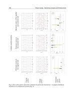
Fig. 3. Output waveforms of ML and MMSE algorithms at 10 dB SNR
Fig. 4. Output waveforms of CC and DT algorithms at 10 dB SNR
Fig. 3 depicts the output waveforms of ML and MMSE algorithms at 10 dB SNR. There are
plateaus and basins in the output waveforms of ML and MMSE, which make the peak
energy ambiguous. It is much easier to find accurate timing information in the output
waveform of CC in Fig. 4. However, there are glitches in CC output waveform, which will
corrupt the detection of symbol boundary and increase the false alarm probability. The
waveform of DT has much lower noise floor compared with CC and there is not any glitch.
0 200 400 600 800 1000
-30
-25
-20
Sample index
ML
0 200 400 600 800 1000
20
25
30
35
Sample index
MMSE
0 200 400 600 800 1000
0
1000
2000
3000
4000
CC
Sample index
0 200 400 600 800 1000
0
2
4
6
x 10
6
DT
Sample index
Glithes
Ultra Wideband Communications: Novel Trends – System, Architecture and Implementation
166
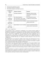
2.3 Architecture of the matched filter
Matched filter is the basic component in timing synchronization for detecting a known piece
of signal in noise. The architecture of mated filter determines the complexity and the power
consumption of the timing synchronizer. An optimum architecture of the matched filter for
OFDM-based UWB is provided, as shown in Fig. 5. To satisfy 528 Msps throughput, the
baseband receiver system of UWB is designed at 132 MHz clock frequency with four parallel
paths and twelve-level pipelines. For low complexity, both the received signal and the
preamble coefficients are truncated to sign-bit. In this case, five-bit multipliers can be
replaced with NXOR gates. In addition, the 128 sign-bits of preamble coefficients are
generated by spreading a 16 sign-bit sequence with an 8 sign-bits sequence as follows
16( 1)
()
1,2, ,16 1,2, ,8
ji ij
sgn c a b
ij
(12)
where a
i
and b
j
are 1 or -1. According to (12), the 128 taps matched filter can be decomposed to
16 taps cascaded with 8 taps, as shown in Fig. 5. With the decomposition, the processing
period of the matched filter can be reduced to 19% and the length of the circle shift register can
be reduced to 20. In CC operation, if the shift register is full, shift the data from address of
[5:20] to [1:16] and save the coming four sign-bits to the address of [17:20]. The data with the
addresses of [1:16], [2:17], [3:18] and [4:19] are distributed to four parallel data paths and cross-
correlated with the coefficients a
i
. This optimum architecture of the matched filter not only
guarantees the high speed, but also reduces the cost of the hardware.
Fig. 5. Architecture of the matched filter for UWB
3. Coarse frequency synchronization
OFDM-based UWB system is sensitive and vulnerable to carrier frequency offset (CFO),
which can be estimated and compensated by coarse frequency synchronization in time
domain. Due to the Doppler Effect, even very small CFO will lead to very serious
accumulated phase shift after a certain period.
3.1 Effects of carrier frequency offset
Define the normalized CFO, ε
f
= Δf/f
s
, as the ratio of CFO to subcarrier frequency spacing.
The received signal with CFO in frequency domain can be expressed as (Moose, 1994)
Synchronization Technique for OFDM-Based UWB System
167
2(1)/
,,, ,
sin( )
sin( / )
f
jNN
f
kl kl kl kl ICI
f
RSH e WW
NN
(13)
where S
k,l
, H
k,l
and W
k,l
stand for the transmitted signal, channel impulse response and noise
respectively at k-th subcarrier and l-th symbol. W
ICI
is the noise contributed by inter-carrier
interference (ICI). ICI will not only destroy the orthogonality of the subcarriers in OFDM-
based UWB system, but also degrade SNR. The SNR degradation can be approximated as
(Pollet et al., 1995)
2
10
()
3ln10
s
SNR f
o
E
D
N
(14)
where E
s
/N
o
is the ratio of symbol energy to noise power spectral density.
3.2 Frequency synchronization algorithm
The most straightforward frequency synchronization algorithm is based on AC functions.
CFO can be estimated by the phase difference between two symbols. For traditional OFDM
system, the CFO can be estimated as
1
1*
0
ˆ
()
2
N
f
nknkM
k
N
tan r r
M
(15)
where N is the FFT size and M is the interval of two symbols. If apply traditional AC
algorithm in UWB system, the sliding window length (SWL) is 128. The four-parallel
architecture with 128 SWL will be in high complexity. Shortening the SWL can reduce the
complexity with degradation of the estimation performance. To improve the performance
with low complexity, an optimized AC algorithm is provided by shortening the SWL to 64
and making a sum average over three symbols located at three different subbands, as
expressed in (16).
1* *
1122
11
1
*
12 2
1
ˆ
([ ][] [ ( )][ ]
2
[(2)][2])
LL
f
kk
L
k
NNNN N
tan r k G M r k r k G G M r k G M
GM L L L L
NN
rkG GMr kGM
LL
(16)
where L denotes the SWL of each symbol. The values of G
i
(i = 1,2) depend on TFC. If TFC is
{1 2 3 1 2 3} or {1 3 2 1 3 2}, G
1
= 3, G
2
= 1; if TFC is {1 1 2 2 3 3} or {1 1 3 3 2 2}, G
1
= 1, G
2
= 2.
Although the SWL can be further reduced for lower complexity, the performance
degradation requires a much longer period sum average to compensate. Tradeoff in
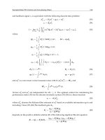
complexity, performance and the processing period, L = 64 is the best choice. Fig. 6 shows
the MSE performance comparison with different SWL. The normalized CFO is set to 0.01.
Due to the sum average over three subbands, the optimized AC algorithm with SWL 64 has
better performance than the traditional AC algorithm with SWL 128. The optimized AC
algorithm with SWL 32 cannot perform as good as traditional AC algorithm with SWL 128.
It needs longer period for sum average to compensate the performance degradation.
For UWB, the CFO compensation algorithm can be optimized as well. The basic idea is to
take the CFO values on four-parallel paths as the same if the differences of the four CFO
Ultra Wideband Communications: Novel Trends – System, Architecture and Implementation
168
values are very small (Fan & Choy, 2010a). In the specification of UWB, the center
frequency is about 4 GHz and the maximum impairment at clock synthesizer is
±20 ppm
(parts per million). Therefore, the normalized CFO should be less than 0.04. And the
maximum CFO difference between any two parallel samples should be less than 2.5 × 10
-4
,
which is small enough and can be ignored. The optimized CFO compensation scheme can
be expressed as
ˆ
[4( 1)][4( 1)](24 )
1,2, , /4 , 1,2,3,4
f
rm
q
rm
q
ex
pj
mM
mMq
(17)
where 4(m-1)+q is the sample index. The optimum CFO compensation strategy not only
reduces the four-parallel digital synthesizer to one, but also alleviates the workload of the
phase accumulator.
Fig. 6. MSE performance comparison with different SWL
3.3 Implementation of frequency synchronizer
The design of frequency synchronizer is divided into two parts. The first part is to estimate
the phase difference between two preambles by AC and arctangent calculation. The second
part is to compensate the signals by multiplying a complex rotation vector. In this part, the
phase accumulator and sin/cos generator are involved.
Fig. 7 shows the architecture of CFO compensation block. The phase accumulator produces
a digital weep with a slope proportional to the input phase. The phase offset is scaled from
[0, 2π] to [0, 8] by multiplying a factor 4/π, so that just the three most significant bits (MSBs)
can be used to control the phase offset regions. During CFO compensation, the sine and
cosine values of the phase offset in the range of [0, π/4] are necessary to be calculated. If the
phase offset is in other ranges, input complement, output complement or output swap are
operated correspondingly.
In the design of frequency synchronizer, implementation of arctangent, sine and cosine
functions is the most critical work since it decides the complexity of the synchronizer and
the performance of the UWB receiver system. The traditional OFDM-based or CDMA-based
5 10 15 20
10
-8
10
-7
10
-6
10
-5
SNR (dB)
MSE
Optim AC L=32
Optim AC L= 64
Traditional AC L=128
Synchronization Technique for OFDM-Based UWB System
169
systems usually employed classic coordinate rotation digital computer (CORDIC) algorithm
for function evaluation (Tsai & Chiueh, 2007; Troya et al., 2008). Actually, there are other
techniques for function evaluation, such as polynomial hyperfolding technique (PHT) (Caro
et al., 2004), piecewise-polynomial approximation (PPA) technique (Caro & Steollo, 2005),
hybrid CORDIC algorithm (Caro et al., 2009) and multipartite table method (MTM) (Caro et
al., 2008).
4
Swapper
Complement
Complement
4
()
ki
r
4
()
ki
r
4
()
ki
r
4
()
ki
r
Rounding
Fig. 7. Architecture of the CFO compensation block
Polynomial hyperfolding technique
PHT calculates sine and cosine functions using an optimized polynomial expression with
constant coefficients. The sine and cosine functions can be expressed by polynomial
expressions of degree K.
1
10
1
10
() ( )
42
() ( )
42
KK
KK
KK
KK
LSB
Sx sin x ax a x a
LSB
Cx cos x bx b x b
(18)
where 0 ≤ x < 1 is the scaled input of sine and cosine functions. Optimization is conducted
on two-order (K = 2) and three-order (K = 3) approximated polynomials, expressed as (19)
and (20) respectively (Caro et al., 2004). The two-order PHT can achieve about 60 dBc
spurious free dynamic range (SFDR) while the three-order PHT can achieve 80 dBc SFDR.
32
252
( ) 0.004713 0.838015 2
( ) 0.9995593 0.011408 ( 2 2 )
Sx x x
Cx x x
(19)
2253
2353
( ) 0.00015005 0.77436217 0.00530040 ( 2 2 ) /3
( ) 0.98423596 0.00452969 0.32417224 (2 2 ) /3
Sx x x x
Cx x x x
(20)
Ultra Wideband Communications: Novel Trends – System, Architecture and Implementation
170
Piecewise polynomial approximation
The technique of PPA is based on the idea of subdividing the interval in shorter
subintervals. Polynomials of a given degree are used in each subinterval to approximate the
trigonometric functions. The signal x represents the input phase scaled to a binary fraction
in the interval of [0, 1], which is subdivided in s subintervals, with s = 2
u
. The u MSBs of x
encode the segment starting point x
k
and are used as an address to the small lookup tables
that store polynomial coefficients. The remaining bits of x represent the offset x – x
k
. The
quadratic PPA of sine and cosine functions can be expressed as (Caro & Steollo, 2005)
2
2
111
() ()()
() ()()
1,2, , ; 0; 1
skk
ss s
ckk
cc c
kk s
kk k
kk k
fx y m x x p x x
fx y m x x p x x
xxx k sx x
(21)
Fig. 9 shows the architecture of sine and cosine blocks with PPA. Use r bits and t bits for the
first-order and the second-order coefficients quantization respectively. The constant
coefficients are (Q – 1) bits. The input and output of the sine and cosine functions are
represented by P bits and Q bits. The constant, linear and quadratic coefficients are read
from ROMs to conduct polynomial calculation. The partial products are generated by the
PPGen block to compute linear terms. And the carry-save addition tree adds the partial
products together after aligning all the bits according to their weights.
Fig. 9. Architecture of sine and cosine blocks with PPA (Caro & Steollo, 2005)
Hybrid coordinate rotation digital computer
This approach splits the phase rotation in three steps. The first two steps are CORDIC-based
with computing the rotation directions in parallel. The final step is multiplier-based (Caro et
al., 2009).
Synchronization Technique for OFDM-Based UWB System
171
Suppose the word length of input vector [X
in
, Y
in
] and output vector [X
out
, Y
out
] are 12 and 13
bits respectively. Represent the rotation phase φ
∈ [0, π/4] with a binary fractional value in
[0, 1] as
12 13
12 13
4
22 2ff f
(22)
The least significant bit (LSB) of φ has a weight that will be indicated in the following as φ
LSB
= (π/4)2
-13
. In the first step, the phase is divided in two subwords φ =
+ β, where
134
13
45 13
45 13
( 2 2 2 )
4
(2 2 2)
4
ff
ff f
(23)
The goal of the first stage is to perform a rotation by an angle close to
+ φ
LSB
/2. To that
purpose, the first rotation uses CORDIC algorithm can be described by the following
equations.
1
1
1
1
2
2 1, ,4
2
i
iii i
i
iii i
i
iii
XX Y
YY X i
ZZ tan
(24)
where σ
i
is equal to the sign of Z
i
. The algorithm starts with X
1
= X
in
, Y
1
= Y
in
and
Z
1
=
+ φ
LSB
/2.
The second and third stages rotate the output vector of the first stage by a phase γ = Z
residual
+ β, which is represented with 11 bits. γ is then split as the sum of two subwords γ
1
+ γ
2
,
where
3123
1012
334 10
234 10
2( 2 2 2)
2( 2 2 2 )
gg g
gg g
(25)
The second rotation is aimed to perform the rotation by the phase γ
1
. The rotation directions
are obtained by the bits of γ
1
as follows.
00
21 211,2
ii
ggi
(26)
The corresponding CORDIC equations are
(4)
'' '
1
(4)
'' '
1
2
0,1,2
2
i
iii i
i
iii i
XX Y
i
YY X
(27)
And the operation to be performed in the final rotation block can be written as
2222
2222
cos sin
sin cos
out T T
out T T
XX Y
YX Y
(28)
Ultra Wideband Communications: Novel Trends – System, Architecture and Implementation
172
where [X
T2
, Y
T2
] is the output vector of the second rotation. The absolute value of γ
2
is
smaller than 2
-6
. Therefore, sine and cosine functions can be approximated as sin γ
2
≈
γ
2
and
cos γ
2
≈ 1.
The architecture of hybrid CORDIC rotator is shown in Fig. 10. The elementary stage is
composed with adders and shifters. The two final vector merging adders (VMAs) convert
the results to two’s complement representation.
Fig. 10. Architecture of hybrid CORDIC technique (Caro et al., 2009)
Multipartite table method
MTM is a very effective lookup table compression technique for function evaluation. It has
been found ideally suited for high performance synthesizer, requiring both very small ROM
size and simple arithmetic circuitry (Caro et al., 2008). The principle of MTM is to
decompose Q-bit input signal x in K + 1 non-overlapping sub-words: x
0
, x
1
, …, x
K
with
lengths of q
0
, q
1
, …, q
K
respectively, where x = x
0
+ x
1
+ … + x
K
and Q = q
0
+ q
1
+ … + q
K
. The
angle [0, π/4] is scaled to a binary fraction in [0, 1]. A piecewise linear approximation of f(x)
can be expressed as
01 0 01
001 0
0111
( ) ( ) ( ) ( )( )
() () ()
() () ( )
KK
K
KKK
f
xfxx x AxBxx x
Ax Bx x Bx x
Ax B x B x
(29)
The interval of x has been divided in 2
q0
subintervals. x
0
represents the starting point of each
subinterval and x
1
+ … + x
K
is the offset in each interval between x and x
0
.
1
is a sub-word
of x
0
including its p
1
≤ q
0
MSBs. Likewise,
i
(i = 2 K) is a sub-word of x
0
including its p
i
≤ p
i
- 1
. The term A(x
0
) can be realized with a ROM, which is named as table of initial values
(TIV), with 2
q0
entries. And the terms B(
i
) x
i
(i = 1…K) can be implemented with K ROMs,
which is named as table of offsets (TO
i
), with 2
pi
+
qi
entries each. Making the TOs symmetric,
the size of ROMs can be reduced by a factor of two. Then, the equation (29) becomes
Synchronization Technique for OFDM-Based UWB System
173
1
0111
() ( ) ( )( ) ( )( )
22
K
KK K
fx Ax B x B x
(30)
where the coefficients can be calculated as follows (Caro et al., 2008).
000
0
1
0
01
0
() ( )
()
2
()()( )( )
()
2
TO ( , ) ( )( 2 )
(2 1)2 ; ; 2 2 ; 2 2
ii i iii ii
ii
i
s
iii ii i
iK
qs pqs q
Q
iiji j
jj
i
ii iii
fx fx
Ax
fff f
B
xB x
sq
(31)
The architecture of MTM with symmetric TOs is shown in Fig. 11. The content of TOs is
conditionally added or subtracted from the content stored in TIV. The addition or
subtraction of the content in ROMs and complement operation of the inputs are controlled
by the MSB of each subword.
Fig. 11. Architecture of MTM with symmetric TOs
In order to give a fair comparison of the four techniques, they are used to implement CFO
compensation block. The parameters of the design are set to make the SFDR of the four
techniques nearly the same. The inputs and outputs of the four algorithms are 12 bits.
Synthesized with UMC 0.13 μm high speed library at 132 MHz clock frequency, the power,
area and latency of the four methods are listed in Table 1. MSE is a statistical value, so it is
not easy to set the MSEs of the four approaches exactly the same. But they are very closed.
With the smallest MSE, MTM outperforms other algorithms in area, power and latency.
Since MTM is proved to be an efficient approach for function evaluation, it can be applied to
implement arctangent fucntion in CFO estimation block.
Ultra Wideband Communications: Novel Trends – System, Architecture and Implementation
174
Technique MTM PPA PHT
Hybrid
CORDIC
Design
parameter
q
0
= 4 q
1
= 2
q
2
= 3 q
3
= 3
p
1
= 3 p
2
= 3
p
3
=1
s = 64
r = 6
t = 7
K = 3
(1) 4 rep.
(2) 3 rep.
(3) 8b × 8b
MSE
(×10
-7
)
2.97 4.91 7.82 5.73
Area
(mm
2
)
0.018 0.027 0.031 0.146
Power
(mW)
0.84 0.88 1.55 13.93
Latency
(Clock cycs.)
3 3 4 6
Table 1. Synthesis performance comparison of CFO compensation with four techniques
4. Fine frequency synchronization
Although CFO can be coarsely estimated by frequency synchronizer in time domain, the
residual CFO (RCFO), sampling frequency offset (SFO) and common phase error will lead to
accumulated phase shift after a certain period and thus degrade the system performance if
they are not carefully tracked. In OFDM-based UWB systems, pilot subcarriers can help to
solve the residual phase distortion issue in frequency domain, which is also called fine
frequency synchronization.
4.1 Effects of sampling frequency offset
The oscillators used to generate the DAC and ADC sampling instants at the transmitter and
receiver will never have exactly the same period. Thus, the sampling instants slowly shift
relative to each other. The SFO has two main effects: a slow shift of the symbol timing,
which rotates subcarriers; and a loss of SNR due to the ICI generated by the slightly
incorrect sampling instants, which causes loss of the orthogonality of the subcarriers.
Define the normalized sampling error as Δt = (T’ - T)/T, where T’ and T are the receiver and
transmitter sampling periods respectively. Then the overall effect on the received signal in
frequency domain is expressed as
2/
,,, ,
() (,)
jktlTT
kl kl kl kl t
su
RSHe sincktWNkl
(32)
where T
s
and T
u
are the duration of the total symbol and the useful data respectively. W
k,
l
is
additive white Gaussian noise (AWGN) and the last term N
Δt
(k, l) is the additional
interference due to the SFO. The power of the last term is approximated by
2
2
()
3
t
Pkt
(33)
Hence the degradation grows as the square of the produce of the offset Δt and the subcarrier
index k. This means that the outermost subcarriers are most severely affected. The
degradation can also be expressed directly by SNR loss as (Pollet et al., 1995)
Synchronization Technique for OFDM-Based UWB System
175
2
2
10
0
10 (1 ( ) ) ( )
3
s
n
E
Dlo
g
kt dB
N
(34)
The OFDM-base UWB system does not have a large number of subcarriers and the value of
Δt is quite small. So kΔt << 1, and the interference caused by SFO can usually be ignored.
However, the term showing the amount of rotation angle experienced by the different
subcarriers will lead to serious problem. Since the rotated angle depends on both the
subcarrier index and symbol index, the angle is the largest for the outermost subcarrier and
increases with the consecutive symbols. Although Δt is very small, with the increasing of the
symbol index, the phase shift will eventually corrupt the demodulation. In this case,
tracking SFO is necessary.
4.2 Phase tracking algorithms
Conventionally, SFO can be estimated by computing a slope from the plot of pilot subcarrier
differences versus pilot subcarrier indices (Speth et al., 2001). Recently, joint estimation of
CFO and SFO has also been studied extensively, such as the linear least squares (LLS)
algorithm (Liu & Chong, 2002) and joint weighted least squares (WLS) algorithm (Tsai et al.,
2005).
Auto-correlation
The reveived signal with residual phase distortion in frequency domain after removing the
channel noise can be modeled as
,,,, , ,
() (( ))
kl kl kl kl kl kl l
ZSPSexpj Sexpjk
(35)
where P
k, l
is the phase distortion vector and Φ
k, l
is the residual phase error. The relationship
of
, β
l
and Φ
k, l
is shown in Fig. 12.
is the slope of the phase distortion and is contributed
by SFO. β
l
is the intercept of phase distortion and is caused by RCFO of symbol l.
The basic idea of AC is to get the phase differences of pilot subcarriers between two
symbols.
Fig. 12. The relationship of phase distortion and subcarriers
The pilot subcarriers are divided into two parts, C
1
and C
2
. C
1
is on the left of the spectrum,
and C
2
is on the right of the spectrum. Then the estimated intercept phase β
l
and the slope
are written as (Speth et al., 2001)
Ultra Wideband Communications: Novel Trends – System, Architecture and Implementation
176
,,
,,
21
12
21
1
ˆ
ˆ
()
2
kl kl
kC kC
lklkl
kC kC
kC kC
kk
(36)
where
1* 1*
,,1,,,,1
12
kl kl kl kl kl kl
kC kC
tan Z Z tan Z Z
(37)
Linear least squares
Applying LLS estimation to (37) with K pilots in one symbol, each pilot is located at the
subcarrier of
k
i
. The RCFO and SFO estimation yield (Liu & Chong, 2002)
,,
11
2
1
ˆˆ
22
KK
i
kl kl
ii
fK
i
i
ii
k
MK MK
k
NN
(38)
where
1*
,,,1
1
K
kl kl kl
i
iii
tan Z Z
(39)
Such an estimation algorithm that is based on the phase differences between two symbols
can remove the common channel fading terms in slow-fade scenarios. Consequently, this
estimation scheme can be applied before channel estimation and equalization.
Weighted least squares
Though the joint LLS estimation algorithm provides accurate estimation results in the
AWGN channel, diverse channel responses on the pilot subcarriers can render its estimation
useless. For instance, phase of several deeply faded pilot subcarriers, when employ the
estimation of the joint LLS, can lead to a large error in the estimation results. On the other
hand, the phases of those subcarriers with little fading are naturally more reliable.
Therefore, weighting the subcarrier data is advantageous, and data of serious faded
subcarriers should be assigned smaller weights to minimize their adverse effect on
estimation accuracy. The WLS algorithm for joint estimation of RCFO and SFO can be
expressed as (Tsai et al., 2005)
2
,,
00 00
2
2
00 0
ˆ
2
KK KK
ii i ii i i
kl kl
ii ii
f
KK K
iii ii
ii i
ii
kkk
MK
kk
N
(40)
,,
00 0 0
2
2
00 0
ˆ
2
KK K K
ii i iii
kl kl
ii i i
KK K
iii ii
ii i
ii
kk
MK
kk
N
(41)
Synchronization Technique for OFDM-Based UWB System
177
The weight ω
i
should be inversely proportional to the variance of phase error, which
depends on noise, ICI and the complex channel gain. Usually, the residual synchronization
error is so small that the ICI term can be neglected and
ω
i
only depends on the channel gain
of the pilot subcarriers. The disadvantage is this algorithm is very complicated, especially
the computation of the parameter of ω
i
. Without estimating the ω
i
accurately, there will be
large error in phase tracking.
Novel approach for UWB
In traditional phase tracking solutions, arctangent, sine and cosine functions are necessary,
which are quite complicated in hardware implementation. The algorithm presented in
(Troya et al., 2007) simplifies the hardware cost significantly compared with the traditional
approaches. However, it sacrifies system performance slightly. In (Fan & Choy, 2010b), a
novel phase tracking method for UWB is proposed. It not only has low complexity, but also
improves the performance.
Considering the condition |
k|<<1 is satisfied with k ∈ [-55, 55], the first order
approximation can be made as
cos(
k) ≈ 1 and sin(
k) ≈
k. Then the phase distortion in (35)
can be rewritten as
,
()
kl l l l l
P cos k sin j sin k cos
(42)
In (42), four parameters are of interests:
sinβ
l
, cosβ
l
,
· sinβ
l
and
· cosβ
l
. The former two can
be easily obtained by
,
25,35,45,55
,
25, 35, 45, 55
1
{}
8
1
{}
8
lkl
k
lkl
k
cos P
sin P
(43)
where
()
and
()
denote the real and imaginary part respectively. There are 12 pilots in
each symbol of OFDM-based UWB system. Since 1/8 is much easier to implement than 1/12
and the pilots near DC subcarrier suffer more channel noise than the ones far away from DC
subcarrier, the pilots outermost should be used as many as possible.
Approximating the scaling factor 1/260 to 1/256, which can be easily implemented by 8-bit
right-shifting, the parameters of
· sinβ
l
and
· cosβ
l
are given by
,,
55, 35 , 25, 15 15,25 ,35,55
,,
55 ,35,25 ,15 15, 25 , 35, 55
1
({}{})
256
1
({} {})
256
lklkl
kk
lklkl
kk
sin P P
cos P P
(44)
In the traditional algorithms, although LLS and WLS algorithms have better phase tracking
performance than AC, they have very high complexity for practical application. For
hardware implementation, AC is in low complexity and moderate phase correction
performance. Therefore, the MSE performance of the novel approach for UWB and AC are
compared in different phase dostrotion conditions, as shown in Fig. 13. Obviously, the novel
phase tracking method for UWB has much better proformance than the traditional AC
Ultra Wideband Communications: Novel Trends – System, Architecture and Implementation
178
algorithm. In addition, with the increasing of phase error, the traditional AC algorithm
degrades seriously, which is not associated with the novel method.
Fig. 13. MSE performance comparison between traditional AC algorithm and the novel
approach for UWB
4.3 Architecture of the phase tracking block
The architecture of phase tracking block with the novel approach for UWB is shown in Fig.
14. The signals after channel equalization are stored in pilots buffer and data buffer
separately. Considering that the transmitted pilots are known and have the modulus of one,
the phase error vector of the pilots can be derived by multiplying the conjugation of
transmitted pilots. As shown in Fig. 14, no arctangent, sine or cosine function appeared, they
are replaced by eight complex adders and two complex shifters.
Pilots
Buffer
Data
Buffer
Transmitted
pilots
( )
*
-12
Accumulator
Z
k, l
,
ˆ
kl
X
MUX
-
3-bit
Shifter
6-bit
Shifter
cosβ
l
+
jsinβ
l
4αsinβ
l
–
j4αcosβ
l
P
-55, l
P
-35, l
P
-25, l
P
-15, l
P
15, l
P
55, l
P
35, l
P
25, l
Phase Error
Estimator
Reg
( )
*
Fig. 14. Highly simplified architecture of the phase tracking block
The values of parameters
· sinβ
l
and
· cosβ
l
are very small, so the phase errors contributed
by SFO of four parallel data can be approximately thought the same, rewritten as
⌈k/4⌉sinβ
l
5 10 15 20
10
-8
10
-7
10
-6
10
-5
SNR (dB)
MSE
AC RCFO=0.004 SFO=5ppm
Novel RCFO=0.004 SFO=5ppm
AC RCFO=0.008 SFO=10ppm
Novel RCFO=0.008 SFO=10ppm
Synchronization Technique for OFDM-Based UWB System
179
and
⌈k/4⌉cosβ
l
(⌈k/4⌉ ∈ [-12, 12]). Calculating the parameters of 4
· sinβ
l
and 4
· cosβ
l
instead of
· sinβ
l
and
· cosβ
l
further simplifies the architecture of phase tracking block.
5. Conclusion
This chapter provides a compreshensive review of the algorithms and architectures for timing
and frequency synchronization. Although there are many literatures on UWB synchronization
techniques, most of them do not take the real application or implementation into account. This
chapter introduces three parts of the synchronizaiton progress.
In timing synchroniztion, DT detection scheme improves the detection performance
significantly due to the cascaded auto-correlator. Although it meanwhile increases the
hardware cost slightly, the optimum architecture of the matched filter with low complexity
can save the hardware. In coarse frequency synchronization, the CFO estimation approach
can be simplified by shortening the SWL and the sum average over three subbands will
compensate the SNR degradation. MTM is proved to be a low cost, low power and high
speed approach to implement arctangent, sine and cosine functions compared with other
function evaluation techniques. In fine frequency synchronization, a novel phase tracking
approach for UWB is proposed for good performance. Additionaly, there is not any
arctangent, sine or cosine intensive computation unit appeared and they are replaced by
adders and shifters, which indicates that the implementation complexity of the novel phase
tracking method is low.
The low compxity and power efficent synchronization techniques provide possibilities of
developing the robust, low cost, low power and high speed OFDM-based UWB receiver.
6. References
Caro, D. D., Napoli, E., & Steollo, A. G. M. (2004). Direct digital frequency synthesizer with
polynomial hyperfolding technique. IEEE Transactions on Circuits and Systems II,
Express Briefs, Vol. 51, No. 7, Jul. 2004, pp. 337-344, ISSN 1549-7747
Caro, D. D, & Steollo, A. G. M. (2005). High-performance direct digital frequency
synthesizer using piecewise-polynomial approximation. IEEE Transactions on
Circuits and Systems I, Regular Papers, Vol. 52, No. 2, Feb. 2005, pp. 324-337, ISSN
1549-8328
Caro, D. D, Petra, N., & Steollo, A. G. M. (2008). Reducing lookup-table size in direct digital
frequency synthesizers using optimized multipartite table method. IEEE
Transactions on Circuits and Systems I, Regular Papers, Vol. 55, No. 7, Aug. 2008, pp.
2116-2127, ISSN 1549-8328
Caro, D. D, Petra, N., & Steollo, A. G. M. (2009). Digital synthesizer/mixer with hybrid
CORDIC-multiplier architecture : error analysis and optimization. IEEE
Transactions on Circuits and Systems I, Regular Papers, Vol. 56, No. 2, Feb. 2009, pp.
364-373, ISSN 1549-8328
Coulson, A. J. (2001). Maximum likelihood synchronization for OFDM using a pilot symbol :
algorithms. IEEE Journal on Selected Areas in Communications, Vol. 19, No. 12, Dec.
2001, pp. 2486-2494, ISSN 0733-8716
Fan, W., Choy, C-S., & Leung K-N. (2009). Robust and low complexity packet detector
design for MB-OFDM UWB. Proceedings of IEEE Int. Symposium on Circuits and
Systems, pp. 693-696
Ultra Wideband Communications: Novel Trends – System, Architecture and Implementation
180
Fan, W., & Choy, C-S. (2010a). Power efficient and high speed frequency synchronizer
design for MB-OFDM UWB. Proceedings of IEEE Int. Conference on UWB, pp. 669-673
Fan, W., & Choy, C-S. (2010b). Efficient and low complexity phase tracking method for MB-
OFDM UWB receiver. Proceedings of IEEE Midwest Symposium on Circuits and
Systems, pp. 221-224
Fort, A., Weijers, J. W., & Derudder, V. et al. (2003). A performance and complexity
comparison of auto-correlation and cross-correlation for OFDM burst
synchronization. Proceedings of IEEE Int. Conference on Acoustics, Speech, and Signal
Processing, pp. 341-344
Liu, S. Y., & Chong, J. W. (2002). A study of joint tracking algorithms of carriers frequency
offset and sampling clock offset for OFDM-based WLANs. Proceedings of IEEE Int.
Conference on Communications, Circuits and Systems and West Sino Expositions, pp.
109-133.
Minn, H., Bhargava, V. K., & Letaief, K. B. (2003). A robust timing and frequency
synchronization for OFDM systems. IEEE Transactions on Wireless Communications,
Vol. 2, No. 4, Jul. 2003, pp. 822-839, ISSN 1536-1276
Moose, P. H. (1994). A technique for orthogonal frequency division multiplexing frequency
offset correction. IEEE Transactions on Communications, Vol. 42, No. 10, Oct. 1994,
pp. 2908-2914, ISSN 0090-6778
Pollet, T., Van Bladel, M., & Moeneclaey, M. (1995). BER sensitivity of OFDM systems to
carrier frequency offset and Wiener phase noise. IEEE Transactions on
Communications, Vol. 43, No. 2, Mar. ~ Apr. 1995, pp. 191-193, ISSN 0090-6778
Schmidl, T. M., & Cox. D. C. (1997). Robust frequency and timing synchronization for
OFDM. IEEE Transactions on Communications, Vol. 45, No. 12, Dec. 1997, pp. 1613-
1621, ISSN 0090-6778
Speth, M., Fechtel, S., & Fock, G. et al. (2001). Optimum receiver design for OFDM-based
broadband transmission-part II: a case study. IEEE Transactions on Communications,
Vol. 49, No. 4, Apr. 2001, pp. 571-578, ISSN 0090-6778
Troya, A., Maharatna, K., & Krstic, M. et al. (2007). Efficient inner receiver design for OFDM-
based WLAN systems: algorithm and architecture. IEEE Transactions on Wireless
Communications, Vol. 6, No. 4, Apr. 2007, pp. 1374-1385, ISSN 1536-1276
Troya, A., Maharatna, K., & Krstic, M. (2008). Low-power VLSI implementation of the inner
receiver for OFDM-based WLAN systems. IEEE Transactions on Circuits and Systems
I, Regular Papers, Vol. 55, No. 2, Mar. 2008, pp. 672-686, ISSN 1549-8328
Tsai, P-Y., Kang, H-Y., & Chiueh, T-D. (2005). Joint weighted least squares estimation of
carrier frequency offset and timing offset for OFDM systems over multipath fading
channel. IEEE Transactions on Vehicular Technology, Vol. 54, No. 1, Jan. 2005, pp. 211-
224, ISSN 0018 9545
Tsai, P-Y., & Chiueh, T-D. (2007). A low-power multicarrier-CDMA downlink baseband
receiver for future cellular communication systems. IEEE Transactions on Circuits and
Systems I, Regular Papers, Vol. 54, No. 10, Oct. 2007, pp. 2229-2239, ISSN 1549-8328
Van de Beek, J. J., Sandell, M., & Borjesson, P. O. (1997). ML estimation of time and
frequency offset in OFDM systems.
IEEE Transactions on Signal Processing, Vol. 45,
No. 7, Jul. 1997, pp. 1800-1805, ISSN 1053-587X
0
Frequency Synthesiz er Architectures for UWB
MB-OFDM Alliance Application
Owen Casha and Ivan Grech
Department of Micro and Nanoelectronics - University of Malta
Malta
1. Introduction
Ultra Wideband (UWB) is an emerging wireless technology supporting data rates as high as
480 Mb/s. As proposed by the MB-OFDM Alliance, the current frequency spectrum for an
UWB communication system ranges from 3.1-to-10.6 GHz divided into 14 bands each with a
528 MHz bandwidth, and are categorised into 5 groups with a strict regulation in emission
power of less than -41 dBm as set by the Federal Communications Commission (FCC). The US
allows the deployment of UWB systems in the whole frequency band, while Japan, Europe,
China and Korea have restricted the use of UWB to a subset of the available frequencies in the
US (Batra et al., 2004a). The current frequency plan of the MBOA-UWB system is shown in
Fig. 1(a) where the highlighted bands are those deployed in Japan, Europe, China and Korea.
An alternative frequency plan is shown in Fig. 1(b) (Mishra et al., 2005).
Fig. 1. (a) Current Frequency Plan and (b) Alternative Frequency Plan of the MBOA-UWB
System (Batra et al., 2004a; Mishra et al., 2005)
Designing frequency synthesizers for UWB MB-OFDM alliance applications faces particularly
stringent challenges and performance criteria. Amongst these one may list the wide range
of frequencies to be synthesized, the in-group frequency hopping time (less than 9.5 ns),
the reduction of the silicon area and the power consumption in the implementation and the
limitation of the integrated spurious tone level in the different bands (less than -32 dBc in a
528 MHz bandwidth). Such challenges cannot be catered for by simply employing standard
frequency synthesizer techniques such as a stand alone phase locked loop (Casha et al., 2009a).
One of the main objectives of this chapter is to study and compare the current state of the
art in frequency synthesis for UWB MBOA applications. On one hand several frequency
synthesizers based on single side band frequency mixing will be discussed. These generally
require multiple phase-locked loops (PLL), complex dividers and mixers to provide adequate
sub-harmonics for the full-band frequency synthesis (Batra et al., 2004b; Mishra et al., 2005).
10
2 Ultra Wideband Communications: Novel Trends
Such architectures are hungry in both silicon area and power consumption. On the other
hand, other novel frequency synthesis architectures being investigated as a low silicon area
alternative will be included in the discussion. These are either based on delay locked loops
(DLL) (Lee & Hsiao, 2005; 2006) or based on phase interpolation direct digital synthesis (DDS)
(Casha et al., 2009a).
The chapter then discusses a study on such frequency synthesizer architectures with special
reference to the investigation of the spurious tone levels at their output. The discussion
is aided by means of mathematically derived analysis tools implemented using Matlab.
These analytic tools provide an adequate system level simulation with low computational
complexity, from which particular design considerations are drawn and are then verified by
means of the design and the simulation of actual circuit building blocks using a particular
integrated circuit technology. The design considerations focus on the reduction of the spurious
tone levels by means of applying different techniques including non-linearity compensation
and dynamic element matching techniques. In addition, based on the observations obtained
from both the analytic tools and the circuit level simulation, the discussion compares the
DLL versus the DDS approach in designing a frequency synthesizer whilst highlighting the
advantages and the disadvantages and commenting on the feasibility of the two architectures.
2. The state of the art - PLL and sideband (SSB) mixer approach
2.1 Architectures
By far, the most common frequency synthesis approach for UWB OFDM frequency synthesis
has been based on dividers and single-sideband (SSB) mixers as proposed in (Batra et al.,
2004b) and depicted in the block diagram shown in Fig. 2. The advantage of this topology
is that it uses just one PLL and allows fast switching between the 3 bands in Group 1. The
first mixer outputs the upper sideband of the 264 and 528 MHz input signals, resulting in the
generation of the 792 MHz signal. A multiplexer is used to select one of the 264 or 792 MHz
signals and input the selected signal into the second mixer. Bands 1 and 2 centre frequencies
are synthesized from the lower sidebands derived by mixing the 4224 MHz signal with 264
or 792 MHz. Band 3 centre frequency is generated by configuring the second mixer for upper
sideband generation and using the 4224 MHz and 264 MHz signal frequencies.
Fig. 2. Synthesis of Group 1 frequency bands using a single PLL, dividers and SSB mixers
(Batra et al., 2004b)
The phase noise from a UWB frequency synthesizer is crucial since interchannel interference
can result if the phase noise performance is poor. In mixer-based synthesizers, the output
182
Ultra Wideband Communications: Novel Trends – System, Architecture and Implementation
Frequency Synthesizer Architectures for UWB MB-OFDM Alliance Application 3
phase noise from a mixer stage can be computed, by assuming that the phase noise in the
inputs of the mixer are uncorrelated and therefore, the output phase noise is given by the
rms sum of the input noise contributions (Mishra et al., 2005). This assumption holds, even
though the signals are derived from the same source, since the delays from the PLL to each
mixer input are significantly different. Typically, the phase noise contribution of the mixer
itself is negligible, since the signal swings involved are orders of magnitude higher than the
mixer thermal noise. Hence the output phase noise L
mix er
at an offset frequency Δ f , of a mixer
stage can be computed from the phase noise levels of the inputs L
1
and L
2
, using Equation 1,
where all noise levels are in dB/Hz relative to the carrier.
L
mix er
(Δ f )=10 log
10
(10
L
1
(Δ f)
10
+ 10
L
2
(Δ f)
10
) (1)
The worst case output phase noise of a mixer-based frequency synthesizer can therefore be
computed by taking into account the synthesis path involving the largest number of frequency
translations. Thus, in the scenario depicted in Fig. 2, the output phase noise L
output
exhibits a
degradation of 0.75 dB relative the PLL phase noise L
PLL
as can be verified from the following
computation:
L
output
(Δ f )=10 log
10
(10
L
PLL
(Δ f)
10
+
10
L
PLL
(Δ f)
10
8
+
10
L
PLL
(Δ f)
10
16
)=10 log
10
(
19
16
•10
L
PLL
(Δ f)
10
) (2)
Mixer-based architectures are investigated to some extent in (Mishra et al., 2005), where
several topologies are discussed, capable of generating all the UWB bands in Groups 1, 3, 4
and 5. Such frequency synthesizer topologies have been adapted and used in complete OFDM
UWB receivers as in (Tanaka et al. (2006), Valdes-Garcia et al. (2006)). In such topologies,
some of the frequency divider stages form path of the feedback path of the PLL itself. It
should be noted, that in order to preserve signal purity, bandpass filters typically have to be
employed at the outputs of the mixers. If frequency selection is carried out before a mixer
stage (as in Fig. 2), then these filters have to be configurable or switchable, making the system
more complex and costly. For this reason, topologies which involve no frequency selection
preceding the mixer stages, tend to be preferred. One such topology is depicted in Fig. 3 and
is capable of generating all bands in groups 1, 2, 3 and 4 (Mishra et al., 2005) of the MB-OFDM
alternate plan. The main advantage of this topology is that the output frequency from the
mixers is fixed and any subsequent filters need not be configurable. Another receiver design
for MB-OFDM application, based on a similar architecture can be found in (Valdes-Garcia et
al., 2007). Other approaches avoid the problems associated with SSB mixing completely, by
having a separate PLL for each band as in (Razavi et al., 2005), where three PLLs are used to
generate the required signals for bands 1 to 3.
Alternative architectures (Roovers et al. (2005), Leenaerts (2005), Lee & Chiu (2005), Liang et
al. (2006), Lee (2006), Leenaerts (2006), Pufeng et al. (2010)) can be found in literature using a
number of PLLs working in parallel. The architecture proposed in (Roovers et al., 2005) and
(Leenaerts, 2005) uses 2 PLLs: one PLL generates a quadrature 3960 MHz signal while the
other PLL generates a quadrature 528 MHz signal. In this way, output quadrature signals of
frequencies 3432, 3960 and 4488 MHz, corresponding to bands 1 to 3 of the MBOA spectrum
are generated. The PLLs have a fixed output frequency and therefore the switching time of
the synthesizer does not depend on the loop bandwidth of the PLLs. In (Lee & Hsiao, 2005),
two parallel PLLs are again employed. The first PLL generates a selectable 6864 or 3432 MHz
output signal while the second PLL generates a selectable 2112 or 1056 MHz signal. Both PLLs
183
Frequency Synthesizer Architectures for UWB MB-OFDM Alliance Application
4 Ultra Wideband Communications: Novel Trends
Fig. 3. Generation of MB-OFDM alternate plan bands 1, 3, 4, 5 (Mishra et al., 2005)
use a 264 MHz reference clock. The output of the second PLL drives a tri-mode divide-by-2
buffer circuit which is capable of generating either a swappable quadrature signal or else a
DC signal. These signals are fed to an SSB mixer which can thus generate output frequencies:
6864, 6864
± 1056, 6864 ± 528, 3432, 3432 ± 1056 and 3432 ± 528 MHz. These frequencies
correspond to bands 1 to 3 and 4 to 7 of the MBOA spectrum, as well as some unused signal
frequencies.
2.2 SSB mixers
SSB mixers can be designed around two Gilbert multiplier cells with the second multiplier
driven by the corresponding quadrature signals as shown in Fig. 4 (Ismail & Abidi, 2005a;b).
The matrix in Equation 3 shows that quadrature outputs can also be generated.
⎛
⎝
cos(ω
1
−ω
2
)t
cos
(ω
1
+ω
2
)t
sin
(ω
1
+ω
2
)t
sin
(ω
1
−ω
2
)t
⎞
⎠
=
⎛
⎝
cos(ω
1
t) sin(ω
1
t)
cos(ω
1
t) −sin(ω
1
t)
sin(ω
1
t) cos(ω
1
t)
sin(ω
1
t) −cos(ω
1
t)
⎞
⎠
×
cos(ω
2
t)
sin(ω
2
t)
(3)
The upper or the lower SSB signal is selected, by reversing the polarity of the outputs of the
second multiplier. Spurious signals can occur if the two mixers are not adequately matched.
Furthermore, emitter-resistor degeneration may be employed in order to improve linearity
of the mixer (Roovers et al., 2005). It is in fact essential that at least one port of the mixer
is linear in order to prevent mixing with harmonics of that input. It is also important that
the inputs themselves exhibit a low distortion level. Furthermore, different delay paths will
also lead to the generation of spurs, while a DC offset on one port will cause leakage of the
other input signal to the output. The linearity requirements often lead to a mixer design with
low conversion gain and low signal swing, often requiring power (and area) hungry buffers.
These problems are particularly troublesome in CMOS technology (Razavi et al., 2005). For
multiple-band output operation, selection of the tank circuit resonant frequency is essential.
In (Zheng & Luong, 2007), this is achieved by having switchable LC sections, controlled by
MOS switches: in this way high Q-factor LC sections can still be used for multiple frequency
184
Ultra Wideband Communications: Novel Trends – System, Architecture and Implementation
Frequency Synthesizer Architectures for UWB MB-OFDM Alliance Application 5
operation. The use of RC polyphase filters for harmonic suppression, as well as phase and
amplitude adjustment has also been investigated (Jiang et al., 2010).
Fig. 4. SSB mixer based on two Gilbert Multiplier Cells
Gain and phase mismatches can also arise when the signals travel through different paths.
In order to compensate for this non-ideality, the use of a vector-calibrated clock buffer
(Lu & Chen, 2005) has been investigated. This buffer essentially adds one of the two
quadrature signals in a controlled manner. In order to achieve this, the tail current of one
of the differential pairs is controlled digitally via a 4-bit DAC. The use of sub-harmonic
mixing has also been investigated in literature (Lin & Wang, 2005a), where eight phases of
a 2.244 GHz signal are generated via the use of a 4-stage ring oscillator. These phases are
mixed with 2.112 and 1.056 GHz signals in order to generate the 3.432, 3.960 and 4.488 GHz
carriers via sub-harmonic mixer, based on Gilbert cells with switchable differential pairs.
When generating the 4.488 GHz carrier, the sub-harmonic mixer actually functions as an
edge-combiner.
2.3 Signal select multiplexers
Signal multiplexers are typically implemented as a number of differential pairs driving the
same load. At any point in time, only one differential pair is enabled by activating its tail
current source. One such topology, reported in (Ismail & Abidi, 2005a;b), is shown in Fig. 5.
2.4 Frequency dividers
2.4.1 Divide-by-2 circuits
High speed divide-by-2 circuits can be implemented using pairs of D-FFs, based on latched
differential pairs, cascaded in master-slave configuration. These master-slave D-FFs are
configured as T-FFs by feeding back the complimentary outputs. The concept is shown in
Fig. 6 as documented in (Ismail & Abidi, 2005b). It should be noted that quadrature signals
are available after at the first (master) stage outputs. Differential-pair buffers are often used to
couple the outputs of the divider circuits to subsequent dividers or mixers (Leenaerts, 2005).
2.4.2 Tri-mode divider
The concept of the tri-mode divider (Lee, 2006) is essentially an extension of the divide-by-2
circuit which incorporates inherent multiplexing such that it permits swappable quadrature
outputs (clockwise and anticlockwise variations) as well as the generation of a DC output.
185
Frequency Synthesizer Architectures for UWB MB-OFDM Alliance Application
6 Ultra Wideband Communications: Novel Trends
Fig. 5. Signal Select Multiplexer implemented using switched differential pairs (Ismail &
Abidi, 2005b)
Fig. 6. Divide-by-2 circuit based on Master-Slave D-FFs
This is achieved by introducing switches in the input stages of the dividers which essentially
select a differential pair which is connected either to the input clock signal, or its complement,
or else to a DC signal. In this way, this type of divider can be used to select between three
different bands as depicted in Fig. 7.
Fig. 7. Tri-Mode Divider Concept for Band-Selection (Lee, 2006)
186
Ultra Wideband Communications: Novel Trends – System, Architecture and Implementation
Frequency Synthesizer Architectures for UWB MB-OFDM Alliance Application 7
A block diagram of the final tri-mode divider is shown in Fig. 7 (Lee, 2006). A practical
CMOS implementation is shown in Fig. 8. The circuit allows for clockwise (CW) and
counter-clockwise (CCW) quadrature signal generation, by flipping the corresponding
quadrature signal in relation to the input clocking signal clk(2ω
1
). In addition, the divider
also allows for DC signal generation. The operation mode is selected by enabling the CW
Select, CCW-Select or DC-Select signals respectively, which effectively steer the tail current
source to the required section to be used.
Fig. 8. CMOS implementation or the trimod divider/buffer
2.4.3 Regenerative (Miller) divider
A Miller divider is based on a feedback loop around a filter with a mixer driven by the
input and feedback signals. This topology has been used in some designs intended for UWB
application (Lin & Wang (2005b),Lee & Huang (2006)). In (Lee & Huang, 2006), the three
different Miller-based dividers, depicted in Fig. 9 are discussed.
Fig. 9. (a) Miller Divider, (b) Modified Miller Divider and (c) Combined Miller/modified
Miller divider (Lee & Huang, 2006)
It can be shown that for the topologies shown in Fig. 9, the following relationships do hold:
187
Frequency Synthesizer Architectures for UWB MB-OFDM Alliance Application
8 Ultra Wideband Communications: Novel Trends
Mill er Divider : F
out
= F
in
− F
out
⇒ F
out
= F
in
/2
Modified Mill er Divider : F
out
= F
in
− F
out
± F
2
⇒ F
out
=(F
in
± F
2
)/2
Combined Mill er Divider/Modi f ied Mill er Divider :
F
out
= F
in
− F
out
± F
in
/N ⇒ F
out
= F
in
(1 ± N)/2 or F
out
= F
in
/2
(4)
In the latter two cases, two frequencies are theoretically possible, but the actual frequency
which is sustained by the loop is selected by the centre frequency of the BPF. The design
proposed in (Lee & Huang, 2006) makes use of a gyrator-based tuned circuit for the BPF, where
the effective inductance of the gyrator circuit is controlled by tuning the transconductance: in
this way tuning of the operating frequency is possible. In this case, the input signal F
in
is
generated by a PLL operating at 7.92 GHz, while N is set to 7.5. In this way the 3432, 3960 and
4488 MHz UWB bands can be generated.
2.4.4 Non-integer (Half-cycle) dividers
Some architectures (Lee & Huang (2006), Van de Beek et al. (2006)) entail the use of
non-integer dividers. Specifically a divide-by-7.5 circuit is used in (Lee & Huang, 2006)
while a divide-by-1.5 circuit is used in (Van de Beek et al., 2006). In (Lee & Huang, 2006),
a specific D-flipflop design is used with selectable positive or negative edge-triggering mode.
The edge-triggering mode is selected via feedback signal as shown in Fig. 10.
Fig. 10. Divide-by-7.5 circuit based on selectable edge-triggering mode (Lee & Huang, 2006)
The approach in (Van de Beek et al., 2006), depicted in Fig. 11 uses multiplexors for the
selection of the appropriate signal used to clock the D-flipflops in the divider.
Fig. 11. Divide-by-1.5 circuit based on multiplexors with quadrature input signals (Van de
Beek et al., 2006)
2.4.5 ROM-based dividers
Dividers based on ROM lookup tables (LUTs) have been proposed for UWB application
(Sandner et al., 2005). In this case the UWB generation circuit is driven by a single PLL
running at 8.448 GHz, which is subsequently divided by two. The resulting 4.224 GHz signal
is used for addressing ROM LUTs storing values of quadrature generation of
±264 or 792 MHz
188
Ultra Wideband Communications: Novel Trends – System, Architecture and Implementation