Semiconductor Technologies Part 2 pptx
Bạn đang xem bản rút gọn của tài liệu. Xem và tải ngay bản đầy đủ của tài liệu tại đây (2.41 MB, 30 trang )
SEMICONDUCTORPROCESSESANDDEVICESMODELLING 23
MOS system begins very important for research the tunnelling current in EEPROM devices
and also in high performance MOS devices with ultra thin oxides (Cassan, 2000).
9.2 The gate leakage currents
The charge distribution and quantum-mechanical leakage currents in ultra thin metal-
insulator-semiconductor gate stacks composed of several layers materials are very
important (Yeo, 2002). Considering all the capacitor like a single quantum mechanical
quantity the effective mass approximation for the electrons in the different valley and the
Hartree approximation for the electron-electron interaction in inversion layer, the
Schrödinger-Poisson equation can be solved. Because the insulating layer is relatively thin
but the energy barriers separating the inversion layer from the gate electrode is high enough
to prevent the flow of electrons to the gate, the potential well host the majority of inversion
layer electrons and the channel is coupled only weakly with the gate (Magnus, 2000).
9.3 The iterative approximation method
The first fully numerical self-consistent results of the inverted MOS structure were mainly
attributed to Stern. Then the self–consistent solution has been extended to holes in inverted
pMOS structure by Moglestue. The quantum mechanical treatment of the MOS structure in
the accumulation regime was described by Sune (Sune, 1992). The self-consistent
Schrödinger-Poisson equations were applicable to an inverted structure in the next
approximations: the effective mass approximation, the ideal interface semiconductor-oxide
and interruption of wave function at interface semiconductor-oxide. The time-independent
Schrödinger equation in 3D space, using the position vector R=(r, z) can be formally written:
H
(r, z) = E(r, z),
(46)
where
(r,z) is the wave function, E is the eigenvalue energy, H is the system Hamiltonian,
composed from kinetic energy T and potential energy W. For long channel device the
potential profile is mainly one dimensional and the drain and source regions can be
considered like electrons reservoirs for the inversion layer. The 1D simplification allows
using the wave operator like a function of the z coordinate only:
(r,z) = (z)e
ik
r
,
(47)
where k=(k
x
,k
y
) is the wave vector in the (x,y) plane. So the carrier are quantized in the z
direction and are free to move in the r=(x,y) plane, with a continuous energy component.
After phase transformation and imposing the constraint of vanishing for the first derivative
of the wave function, the envelope 1D time-independent reduced equation (46) is:
zWz
E
m
z
zz
"
2
2
(48)
where
is reduced Planck constant, m
zz
is the effective masses in m
o
units, W is potential
energy,
(z) is the 1D envelope wave functions and E
z
is the eingenvalue energy.
Considering the MOS structure a quantum mechanical system, an externally applied gate
bias induces a potential well that confines carriers in the region of the semiconductor-oxide
interface. The electrostatic potential and charge respect the Poisson equation in any z
direction from silicon region:
z
d
zV
k
z
d
Si
0
2
2
1
)(
(49)
where V(z) is the electrostatic potential,
(z) is the charge density, k
Si
is the Si relative
dielectric constant. Assuming the p-type substrate with completely ionized impurities and
neglecting the hole concentration in inversion can approximate the charge density:
(z) =
depl
(z) – qn(z),
(50)
where
depl
is the depletion layer charge and n(z) is the carrier’s distribution.
Close to the interface the electrons have a position dependent concentration proportional
with the probability density and a sum of each energy valley and subband.
ji
Fijz
D
ij
ji
ji
z
EE
N
z
n
zn
,
2
,
)2(
,
,
,
(51)
where N
ij
(2D)
is the subband population which integrates the all possible energies of a
subband of the 2D density of states,
z
2
is the probability density, E
z,ij
is the solution of 1D
Schrödinger equation (48) and represents the discrete bottom level of a particular energy
subband j, for each valley i and E
F
is Fermi energy level. The carrier’s distribution can be
more detailed using the valley and spin degeneracy and Fermi-Dirac statistics. The
assumption that the silicon-oxide interface is ideally, was technologically realized by
election the [001] surface orientation that minimizes the dangling bonds at the interface,
resulting a high quality interface after passivation (Babarada, 2008).
Considering the quantization effects of silicon-insulator interface an approximate
geometrical solution to calculate the charge densities and subband energy levels reduces
consistently the computational complexity for leakage current evaluation. Using the same
effective mass approximation the areal density of charge in the inversion layer is:
N
inv
=
ji
z
Fijz
D
ij
dzz
EE
N
,
2
,
)2(
,
=
ji
Fijz
D
ij
EE
N
,
,
)2(
,
(52)
Using the geometrical approximation of Si band bending in inversion (Muller, 1997) the
energy level is:
E
z,ij
=
4
3
2
3
,
2
2
3/2
3/1
j
F
ef
q
m
iz
(53)
and the subband charge is:
q
ij
=
F
q
E
ef
ijz
3
2
,
,
(54)
where F
ef
is the E
z,ij
corresponding effective electric field. Then the inversion charge is:
q
inv
=
ji
inv
D
ji
ji
N
N
q
,
)2(
,
,
,
(55)
and the total silicon surface bending:
S
=
D
+ q
q
T
k
k
q
N
B
Si
inv
inv
0
(56)
where
S
is the surface potential,
D
is the drop voltage at surface due to space charge
region. The last term is the influence of doping concentration to charge region (Muller,
1997). Using the charge boundary conditions the equations can be iteratively solved to attain
the convergence in the next sequence:
Guess the initial N
inv
,
S
and
D
Consider charge boundary condition N
inv-bc
Iterate
S
with condition N
inv
(
S
)/N
inv-bc
1
Iterate
D
with condition
D
0
SemiconductorTechnologies24
Compute the potential distribution
We have possible loops from out to input, of step 3 and 4 and from out of step 4 to input of
step 3. The method can be used also for tunnelling based leakage currents in high-k
dielectric stach.
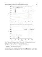
9.4 Results
For numerical simulations we used the ATLAS devices simulator software package from
Silvaco. The main module program used is presented in fig. 20, in order to generate the
MOS structure presented in fig. 21.
Then was calculated the gate current, fig. 22 and the capacity from gate to substrate, fig. 23,
function of polysilicon doping concentrations 10
19
cm
-3
, 10
20
cm
-3
and 10
21
cm
-3
.
mesh
x.mesh loc=-0.01 spac=0.01
x.mesh loc=0.01 spac=0.01
y.mesh loc=-0.04 spac=0.001
y.mesh loc=0.02 spac=0.001
region number=1 x.min=-0.01 x.max=0.01 y.min=-0.04 y.max=-0.03 \
material=aluminum
region number=2 x.min=-0.01 x.max=0.01 y.min=-0.03 y.max=-0.005 \
material=poly
region number=3 x.min=-0.01 x.max=0.01 y.min=-0.005 y.max=0.0 \
material=oxide
region number=4 x.min=-0.01 x.max=0.01 y.min=0.0 y.max=0.02 \
material=silicon
electrode x.min=-0.01 x.max=0.01 y.min=-0.04 y.max=-0.03 name=gate
electrode bottom name=substrate
doping region=2 p.type concentration=1e19 uniform
doping region=4 p.type concentration=1e17 uniform
solve init
solve vgate=-1.5
solve vgate=-3
save outfile=mos2ex15-3V19.str
# tonyplot mos2ex15-3V19.str -set mos2ex15_BD.set
log outfile=mos2ex15_CV19.log
solve vgate=-2.8 vstep=0.2 vfinal=3.0 name=gate ac freq=1e6 previous
tonyplot mos2ex15_CV19.log -set mos2ex15_CV.set
Fig. 20. The main ATLAS program module
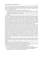
Fig. 21. The device structure Fig. 22. The Gate Current
The first numerical simulations proves the dependence of leakage current, fig. 22 and
depletion effect fig. 23, function of doping concentration like considered in chapter 9.3.
Using the barrier height of 3.1eV, substrate doping 5x10
17
cm
-3
, effective silicon oxide mass of
0.5m
o
and donor poly doping 6x10
19
the results of short computation iterative
approximation, fig. 24, of silicon oxide current gate density calculated ( 1.5nm and 2nm )
was in good agreement with experimental gate current density curves presented in (Yang,
2000) and noted [9] ( 1.41nm[9] and 1.95nm[9] ).
1.00E-08
1.00E-07
1.00E-06
1.00E-05
1.00E-04
1.00E-03
1.00E-02
1.00E-01
1.00E+00
1.00E+01
1.00E+02
1.00E+03
0 0.2 0.4 0.6 0.8 1 1.2 1.4 1.6 1.8 2
Gate voltage, [V]
Gate current density, Jg[A/cm2]
1.5nm
1.41nm[9]
2nm
1.95nm[9]
Fig. 23. The Gate-Substrate Capacity Fig. 24. Silicon oxide gate current density
A little overestimation of leakage current at high gate bias voltage is observed also in other
reports (Buchanan, 2000), based of approximation of Fermi level by the value in the bulk
silicon substrate.
1.00E-02
1.00E-01
1.00E+00
1.00E+01
1.00E+02
1.00E+03
1.00E+04
1.00E+05
1.00E+06
1.00E+07
0.4 0.6 0.8 1 1.2 1.4 1.6 1.8
Echivalent oxide thicknes s, EOT [nm]
Current density, Jg[A/cm2]
SiO2
SiO2-ITRS
SiON
SiON-ITRS
1.00E-08
1.00E-07
1.00E-06
1.00E-05
1.00E-04
1.00E-03
1.00E-02
1.00E-01
1.00E+00
0 0.5 1 1.5 2 2.5
Gate bias, Vg [V]
Current density, Jg[A/cm2]
1.5nm
1.51nm[12]
1.8nm
1.85nm[12]
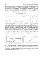
Fig. 25. Oxide and oxynitride leakage current Fig. 26. Al
2
O
3
high-k stacks leakage currents
The polysilicon doping level suppresses the gate leakage current for gate bias in inversion
because the additional voltage drops over the depleted layer (Yang, 2000). This solution
decreases the drive capacitance and the device performances. The substrate doping level
affects the leakage current through the surface potential of the channel. Because increasing
the physical thickness of gate dielectric affects the device parameters like drive current, a
SEMICONDUCTORPROCESSESANDDEVICESMODELLING 25
Compute the potential distribution
We have possible loops from out to input, of step 3 and 4 and from out of step 4 to input of
step 3. The method can be used also for tunnelling based leakage currents in high-k
dielectric stach.
9.4 Results
For numerical simulations we used the ATLAS devices simulator software package from
Silvaco. The main module program used is presented in fig. 20, in order to generate the
MOS structure presented in fig. 21.
Then was calculated the gate current, fig. 22 and the capacity from gate to substrate, fig. 23,
function of polysilicon doping concentrations 10
19
cm
-3
, 10
20
cm
-3
and 10
21
cm
-3
.
mesh
x.mesh loc=-0.01 spac=0.01
x.mesh loc=0.01 spac=0.01
y.mesh loc=-0.04 spac=0.001
y.mesh loc=0.02 spac=0.001
region number=1 x.min=-0.01 x.max=0.01 y.min=-0.04 y.max=-0.03 \
material=aluminum
region number=2 x.min=-0.01 x.max=0.01 y.min=-0.03 y.max=-0.005 \
material=poly
region number=3 x.min=-0.01 x.max=0.01 y.min=-0.005 y.max=0.0 \
material=oxide
region number=4 x.min=-0.01 x.max=0.01 y.min=0.0 y.max=0.02 \
material=silicon
electrode x.min=-0.01 x.max=0.01 y.min=-0.04 y.max=-0.03 name=gate
electrode bottom name=substrate
doping region=2 p.type concentration=1e19 uniform
doping region=4 p.type concentration=1e17 uniform
solve init
solve vgate=-1.5
solve vgate=-3
save outfile=mos2ex15-3V19.str
# tonyplot mos2ex15-3V19.str -set mos2ex15_BD.set
log outfile=mos2ex15_CV19.log
solve vgate=-2.8 vstep=0.2 vfinal=3.0 name=gate ac freq=1e6 previous
tonyplot mos2ex15_CV19.log -set mos2ex15_CV.set
Fig. 20. The main ATLAS program module
Fig. 21. The device structure Fig. 22. The Gate Current
The first numerical simulations proves the dependence of leakage current, fig. 22 and
depletion effect fig. 23, function of doping concentration like considered in chapter 9.3.
Using the barrier height of 3.1eV, substrate doping 5x10
17
cm
-3
, effective silicon oxide mass of
0.5m
o
and donor poly doping 6x10
19
the results of short computation iterative
approximation, fig. 24, of silicon oxide current gate density calculated ( 1.5nm and 2nm )
was in good agreement with experimental gate current density curves presented in (Yang,
2000) and noted [9] ( 1.41nm[9] and 1.95nm[9] ).
1.00E-08
1.00E-07
1.00E-06
1.00E-05
1.00E-04
1.00E-03
1.00E-02
1.00E-01
1.00E+00
1.00E+01
1.00E+02
1.00E+03
0 0.2 0.4 0.6 0.8 1 1.2 1.4 1.6 1.8 2
Gate voltage, [V]
Gate current density, Jg[A/cm2]
1.5nm
1.41nm[9]
2nm
1.95nm[9]
Fig. 23. The Gate-Substrate Capacity Fig. 24. Silicon oxide gate current density
A little overestimation of leakage current at high gate bias voltage is observed also in other
reports (Buchanan, 2000), based of approximation of Fermi level by the value in the bulk
silicon substrate.
1.00E-02
1.00E-01
1.00E+00
1.00E+01
1.00E+02
1.00E+03
1.00E+04
1.00E+05
1.00E+06
1.00E+07
0.4 0.6 0.8 1 1.2 1.4 1.6 1.8
Echivalent oxide thicknes s, EOT [nm]
Current density, Jg[A/cm2]
SiO2
SiO2-ITRS
SiON
SiON-ITRS
1.00E-08
1.00E-07
1.00E-06
1.00E-05
1.00E-04
1.00E-03
1.00E-02
1.00E-01
1.00E+00
0 0.5 1 1.5 2 2.5
Gate bias, Vg [V]
Current density, Jg[A/cm2]
1.5nm
1.51nm[12]
1.8nm
1.85nm[12]
Fig. 25. Oxide and oxynitride leakage current Fig. 26. Al
2
O
3
high-k stacks leakage currents
The polysilicon doping level suppresses the gate leakage current for gate bias in inversion
because the additional voltage drops over the depleted layer (Yang, 2000). This solution
decreases the drive capacitance and the device performances. The substrate doping level
affects the leakage current through the surface potential of the channel. Because increasing
the physical thickness of gate dielectric affects the device parameters like drive current, a
SemiconductorTechnologies26
compromise solution is to increase the dielectric constant using the SiON layer with
dielectric constant up to 7.6 for Si
3
N
4
. The performances of SiON like gate dielectric are
better than SiO
2
as in fig. 25, according with simulations at Vg=1V and ITRS. Comparing the
calculated data with gate leakage current through Al
2
O
3
high-k dielectric stacks presented in
(Buchanan, 2000) a good fit was obtained, fig. 26.
9.5 Conclusions
High-k atomic layer deposition stacks like insulating in the metal-insulating-semiconductor
structure was studied. An iterative approximate method to calculate the 1D MOS structures
main electric parameters without using the Schrödinger-Poisson equations was used. This
method is based on approximation of effective field function of doping parameters. The
tunnelling currents can be calculated more rapidly and the study for different gate dielectric
stacks can be made. The precision can be increased by 2D or 3D analysis of Schrödinger-
Poisson equations. The main application is to calculate the direct tunnelling current due to
the thin oxide layers. The method is extensible to high-k dielectric stacks in order to study
the influence of several material parameters like the impact of layer thickness on gate
leakage and the approach of gate stack scalability. The results obtained using numerical
calculation show that the increase of the gate dielectric constant has a very important effect
in reducing the leakage currents. Comparing the results from fig. 24 and fig. 26 for 1V gate
bias and 1.5nm thickness the increase of dielectric constant to 7 reduce the leakage current
with 4 order of magnitude. Other simulations show that the leakage current decrease
significant when the interfacing oxide is completely eliminated. Future works will be focus
of other high-k dielectric stacks like HfO
2
, HfSiO
4
, ZrSiO
4
, La
2
O
3
, and Y
2
O
3
.
10. References
Babarada, F.; et all. (2003). Carrier Mobility and Series Resistance MOSFET Modelling,
BioMEMS and Nanotechnology, vol. 5275-49, pp. 354-363, SPIE’s, Perth, Australia
Babarada, F.; et all. (2005). MOSFET Conductance Modelling Including Distortion Analysis
Aspects, Proceedings of the International Conference, Sinaia, România
Babarada, F.; Plugaru, R.; Rusu, A. (2008). Electrical characterization of atomic layer high-k
dielectic gate for advanced CMOS devices, Proceedings of the International Conference,
pp. 363-366, ISBN 978-1-4244-2004-9, Sinaia, România
Buchanan, D.A.; et all. (2000). 80 nm poly-silicon gated n-FET with ultra thin Al
2
O
3
gate
dielectric for ULSI applications, IEDM Tech. Dig., pp. 223-226, San Francisco, USA
Bucher, M.; et all. (2007). A Scalable Advanced RF IC Design-Oriented MOSFET Model, Int.
Journal of RF and Microwave Computer-Aided Engineering, DOI 10.1002/mmce
Campian, I.; Profirescu, O.; Babarada, F.; Lakatos, E. (2003). MOSFET Simulation-TCAD
Tools/Packages, Proceedings of the Int. Conf., pp. 235-238, Sinaia, România
Cassan, E. (2000). On the reduction of direct tunnelling leakage through ultra-thin gate
oxides by one-dimensional Schr Poisson solver, J. Appl. Phys. 87(11), pp. 7931-7939
Gildenblat, G.; Zhu, Z.; McAndrew, C. (2009). Surface potential equation for bulk MOSFET,
Solid-State Electronics, 53: pp. 11-13
Govoreanu, B.; et all. (2002). On the use of Bayesian Neural Networks for TCAD Empirical
Modeling, Romanian Journal Science and Technology, pp.329-338, vol 5, no 4, România
Kwong, M.; Kasnavi, R.; Grifin, P.; Duton, R. (2002). Impact of Lateral Source/Drain
Abruptness on Device Performance, IEEE Trans. on El. Dev., vol. 49, no. 11.
Lo, S.; Buchanan, D.; Taur, Y.; Wang, W (1997). Quantum mechanical modelling of electron
tunnelling current from the inversion layer of ultra-thin-oxide nMOSFET, IEEE El.
Dev. Lett., 18(5), pp. 209-211
Magnus, W.; Schoenmaker, W.; (2000). Full quantum mechanical model for the charge
distribution and the leakage currents in ultrathin metal-insulator-semiconductor
capacitors, J. Appl. Phys. 88(10), pp. 5833-5842
Muller, H.; Schultz, M. (1997). Simplified method to calculate the band bending and the
subband energies in MOS capacitors, IEEE Trans. El. Dev. 44(9), pp. 1539-1543
Rusu, A. (1990). Microelectronics Active Components Modelling, Editura Academiei Române
Scholten, A.J.; et all. (2009). The new CMC standard compact MOS model PSP: advantages
for RF applications, IEEE Journal of Solid-State Circuits, vol. 44, no. 5, pp. 1415-1424
Sune, J.; Olivio, P.; Ricco, B. (1992). Quantum mechanical modelling of accumulation layers
in MOS structures, IEEE Trans. El. Dev., 39(7), pp. 1732-1739
Veendrick, H. (2008). Nanometer CMOS ICs: From Basics to ASICs, Springer, ISBN 978-1-4020-
8332-7, Netherland
Yang, N.; Henson, W.; Wortman, J. (2000). A comparative study of gate dielectric tunnelling
and drain leakage currents in n-MOSFET with sub-2-nm gate oxides, IEEE Trans.
El. Dev. 47(8), pp. 1636-1644
Yeo, Y.; King, T.; Hu, C.; (2002). Direct tunnelling leakage current and scalability of
alternative gate dielectrics, Appl. Phys. Lett., 81(11), pp. 2091-2093
Ytterdal, T.; Cheng, Y.; Fjeldly, T. (2003). Device Modeling for Analog and RF CMOS Circuit
Design, J. Wiley, ISBN 0-471-49869-6, England
SEMICONDUCTORPROCESSESANDDEVICESMODELLING 27
compromise solution is to increase the dielectric constant using the SiON layer with
dielectric constant up to 7.6 for Si
3
N
4
. The performances of SiON like gate dielectric are
better than SiO
2
as in fig. 25, according with simulations at Vg=1V and ITRS. Comparing the
calculated data with gate leakage current through Al
2
O
3
high-k dielectric stacks presented in
(Buchanan, 2000) a good fit was obtained, fig. 26.
9.5 Conclusions
High-k atomic layer deposition stacks like insulating in the metal-insulating-semiconductor
structure was studied. An iterative approximate method to calculate the 1D MOS structures
main electric parameters without using the Schrödinger-Poisson equations was used. This
method is based on approximation of effective field function of doping parameters. The
tunnelling currents can be calculated more rapidly and the study for different gate dielectric
stacks can be made. The precision can be increased by 2D or 3D analysis of Schrödinger-
Poisson equations. The main application is to calculate the direct tunnelling current due to
the thin oxide layers. The method is extensible to high-k dielectric stacks in order to study
the influence of several material parameters like the impact of layer thickness on gate
leakage and the approach of gate stack scalability. The results obtained using numerical
calculation show that the increase of the gate dielectric constant has a very important effect
in reducing the leakage currents. Comparing the results from fig. 24 and fig. 26 for 1V gate
bias and 1.5nm thickness the increase of dielectric constant to 7 reduce the leakage current
with 4 order of magnitude. Other simulations show that the leakage current decrease
significant when the interfacing oxide is completely eliminated. Future works will be focus
of other high-k dielectric stacks like HfO
2
, HfSiO
4
, ZrSiO
4
, La
2
O
3
, and Y
2
O
3
.
10. References
Babarada, F.; et all. (2003). Carrier Mobility and Series Resistance MOSFET Modelling,
BioMEMS and Nanotechnology, vol. 5275-49, pp. 354-363, SPIE’s, Perth, Australia
Babarada, F.; et all. (2005). MOSFET Conductance Modelling Including Distortion Analysis
Aspects, Proceedings of the International Conference, Sinaia, România
Babarada, F.; Plugaru, R.; Rusu, A. (2008). Electrical characterization of atomic layer high-k
dielectic gate for advanced CMOS devices, Proceedings of the International Conference,
pp. 363-366, ISBN 978-1-4244-2004-9, Sinaia, România
Buchanan, D.A.; et all. (2000). 80 nm poly-silicon gated n-FET with ultra thin Al
2
O
3
gate
dielectric for ULSI applications, IEDM Tech. Dig., pp. 223-226, San Francisco, USA
Bucher, M.; et all. (2007). A Scalable Advanced RF IC Design-Oriented MOSFET Model, Int.
Journal of RF and Microwave Computer-Aided Engineering, DOI 10.1002/mmce
Campian, I.; Profirescu, O.; Babarada, F.; Lakatos, E. (2003). MOSFET Simulation-TCAD
Tools/Packages, Proceedings of the Int. Conf., pp. 235-238, Sinaia, România
Cassan, E. (2000). On the reduction of direct tunnelling leakage through ultra-thin gate
oxides by one-dimensional Schr Poisson solver, J. Appl. Phys. 87(11), pp. 7931-7939
Gildenblat, G.; Zhu, Z.; McAndrew, C. (2009). Surface potential equation for bulk MOSFET,
Solid-State Electronics, 53: pp. 11-13
Govoreanu, B.; et all. (2002). On the use of Bayesian Neural Networks for TCAD Empirical
Modeling, Romanian Journal Science and Technology, pp.329-338, vol 5, no 4, România
Kwong, M.; Kasnavi, R.; Grifin, P.; Duton, R. (2002). Impact of Lateral Source/Drain
Abruptness on Device Performance, IEEE Trans. on El. Dev., vol. 49, no. 11.
Lo, S.; Buchanan, D.; Taur, Y.; Wang, W (1997). Quantum mechanical modelling of electron
tunnelling current from the inversion layer of ultra-thin-oxide nMOSFET, IEEE El.
Dev. Lett., 18(5), pp. 209-211
Magnus, W.; Schoenmaker, W.; (2000). Full quantum mechanical model for the charge
distribution and the leakage currents in ultrathin metal-insulator-semiconductor
capacitors, J. Appl. Phys. 88(10), pp. 5833-5842
Muller, H.; Schultz, M. (1997). Simplified method to calculate the band bending and the
subband energies in MOS capacitors, IEEE Trans. El. Dev. 44(9), pp. 1539-1543
Rusu, A. (1990). Microelectronics Active Components Modelling, Editura Academiei Române
Scholten, A.J.; et all. (2009). The new CMC standard compact MOS model PSP: advantages
for RF applications, IEEE Journal of Solid-State Circuits, vol. 44, no. 5, pp. 1415-1424
Sune, J.; Olivio, P.; Ricco, B. (1992). Quantum mechanical modelling of accumulation layers
in MOS structures, IEEE Trans. El. Dev., 39(7), pp. 1732-1739
Veendrick, H. (2008). Nanometer CMOS ICs: From Basics to ASICs, Springer, ISBN 978-1-4020-
8332-7, Netherland
Yang, N.; Henson, W.; Wortman, J. (2000). A comparative study of gate dielectric tunnelling
and drain leakage currents in n-MOSFET with sub-2-nm gate oxides, IEEE Trans.
El. Dev. 47(8), pp. 1636-1644
Yeo, Y.; King, T.; Hu, C.; (2002). Direct tunnelling leakage current and scalability of
alternative gate dielectrics, Appl. Phys. Lett., 81(11), pp. 2091-2093
Ytterdal, T.; Cheng, Y.; Fjeldly, T. (2003). Device Modeling for Analog and RF CMOS Circuit
Design, J. Wiley, ISBN 0-471-49869-6, England
SemiconductorTechnologies28
IterativeSolutionMethodinSemiconductorEquations 29
IterativeSolutionMethodinSemiconductorEquations
NorainonMohamed,MuhamadZahimSujodandMohamadShawalJadin
x
Iterative Solution Method in
Semiconductor Equations
Norainon Mohamed, Muhamad Zahim Sujod
and Mohamad Shawal Jadin
Universiti Malaysia Pahang, Lebuhraya Tun Razak, 26300 Kuantan, Pahang
Malaysia
1. Introduction
The FEM (sometimes referred to as finite element analysis (FEA)) is a numerical technique
for finding approximate solutions of partial differential equation as well as of integral
equations. The solution approach is based either an approximating system of ordinary
differential equations, which are then solved using standard techniques such as Newton
Method. It is the objective of this paper to describe the application of the method to device
simulation. The device which described in this paper is Silicon Carbide Gate Turn-Off
Thyristor (SiC-GTO Thyristor). The doping profile with the material properties of the device
can be modelled. This paper specifically focuses on the numerical simulation of the device
compare with the common Silicon GTO Thyristor.
The main advantages of the FEM are that conservation laws (e.g., current conservation) are
exactly satisfied even by coarse approximations, it is easy to treat irregular geometries, the
computational mesh can be graded to be fine in regions to rapid change, local mesh
refinement is easier to implement than finite difference method (FDM).
In the following sections, the finite element equations which are arise from the
semiconductor equations are derived and it is shown the equations are the base of
semiconductor device simulations. The implementation of finite element equations will be
discussed in the next section. For detailed discussion of the numerical simulation, it is in the
results and discussion section.
2. Numerical Method
2.1 Semiconductor Equations
The semiconductor equations are a set of five equations that govern the behavior of
semiconductor materials and devices. The set of equations composed of:
Poisson’s equation
d
Npn
q
2
(1)
Current Continuity equations
2
SemiconductorTechnologies30
qR
t
p
q
p
J (2)
qR
t
n
q
n
J
(3)
Drift-Diffusion equations
pDvpq
pp
~
p
J (4)
nDvpq
nn
~
n
J (5)
In these equations, the three unknown quantities are the space-charge potential (
), the
electron (n) and hole (p) densities,
d
N is the doping densities, the constant q is the
magnitude of electronic charge and
is the dielectric permittivity.
p
J and
n
J are the hole
and electron current densities. R is the recombination rate.
p
v
~
and
n
v
~
are the hole and
electron drift velocities.
p
D and
n
D are the hole and electron diffusion coefficients.
The diffusion coefficients and drift velocities are electric field dependent and so the
equations are nonlinear. The recombination term which is also nonlinear may be
approximated by its thermal equilibrium value (Shockley Read Hall Theory).
2.2 Finite Element Equations
To solve (1) to (5), boundary conditions for the space-charge potential and electron and hole
charge carrier densities are required. The finite element equations are derived from (1) to (3)
by multiplying them by
i
(x,y) and integrating over the region Ω occupied by the
device[4].
dsNnpyx
q
dsyx
d
i
)(),(
),(
2
(6)
dsR
t
p
yx
dsyx
q
i
pi
)(),(
),(
1
J
(7)
dsR
t
n
yx
dsyx
q
i
ni
)(),(
),(
1
J
(8)
2.3 Final Form of Equations
In computer solution by the finite element method there are four stages:
1. Read in (or generate internally) material properties- Si and SiC) and element
connectivity (mesh).
2. Assemble the equations (6), (7) and (8) which the finite element equations and
inserting boundary conditions.
3. Solve the resulting linear equations
4. Repeat 2 and 3 iteratively for nonlinear and/or time dependent problems.
3. Simulation Flow
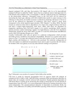
The simulation systems have been implemented by using MATLAB/Simulink surrounding.
The simulation process is used Poisson’s equation together with current continuity and
drift-diffusion equations to simulate the performances of SiC GTO thyristor. Figure 1 shows
the schematic structure of the simulator. Each phase describes complex process which
involves the physical models along with the basic semiconductor equations as the basis to
simulate the GTO performances.
The simulation process is controlled by the Material Input Database in each phase. The red
line indicates the connection with the material database. Material Input Database is
initialized at the initialization process. The basic structure of SiC GTO thyristor is initialized.
The device structure and circuit definitions and additional information like material
properties are loaded from the Material Input Database.
In the next step, the device or the circuit and its embedded devices are loaded and analyzed.
For each segment of each device the material is determined. In the calculations steps, the
basic semiconductor equations along with the physical models are solved by using
numerical method, finite element method. The method is a powerful method for solving
partial differential equations which involves lots of integral and differential. The method is
used because of its approximation to the solution of the equation. In the postprocessing, the
output quantities are calculated from the computed solution.
IterativeSolutionMethodinSemiconductorEquations 31
qR
t
p
q
p
J (2)
qR
t
n
q
n
J
(3)
Drift-Diffusion equations
pDvpq
pp
~
p
J (4)
nDvpq
nn
~
n
J (5)
In these equations, the three unknown quantities are the space-charge potential (
), the
electron (n) and hole (p) densities,
d
N is the doping densities, the constant q is the
magnitude of electronic charge and
is the dielectric permittivity.
p
J and
n
J are the hole
and electron current densities. R is the recombination rate.
p
v
~
and
n
v
~
are the hole and
electron drift velocities.
p
D and
n
D are the hole and electron diffusion coefficients.
The diffusion coefficients and drift velocities are electric field dependent and so the
equations are nonlinear. The recombination term which is also nonlinear may be
approximated by its thermal equilibrium value (Shockley Read Hall Theory).
2.2 Finite Element Equations
To solve (1) to (5), boundary conditions for the space-charge potential and electron and hole
charge carrier densities are required. The finite element equations are derived from (1) to (3)
by multiplying them by
i
(x,y) and integrating over the region Ω occupied by the
device[4].
dsNnpyx
q
dsyx
d
i
)(),(
),(
2
(6)
dsR
t
p
yx
dsyx
q
i
pi
)(),(
),(
1
J
(7)
dsR
t
n
yx
dsyx
q
i
ni
)(),(
),(
1
J
(8)
2.3 Final Form of Equations
In computer solution by the finite element method there are four stages:
1. Read in (or generate internally) material properties- Si and SiC) and element
connectivity (mesh).
2. Assemble the equations (6), (7) and (8) which the finite element equations and
inserting boundary conditions.
3. Solve the resulting linear equations
4. Repeat 2 and 3 iteratively for nonlinear and/or time dependent problems.
3. Simulation Flow
The simulation systems have been implemented by using MATLAB/Simulink surrounding.
The simulation process is used Poisson’s equation together with current continuity and
drift-diffusion equations to simulate the performances of SiC GTO thyristor. Figure 1 shows
the schematic structure of the simulator. Each phase describes complex process which
involves the physical models along with the basic semiconductor equations as the basis to
simulate the GTO performances.
The simulation process is controlled by the Material Input Database in each phase. The red
line indicates the connection with the material database. Material Input Database is
initialized at the initialization process. The basic structure of SiC GTO thyristor is initialized.
The device structure and circuit definitions and additional information like material
properties are loaded from the Material Input Database.
In the next step, the device or the circuit and its embedded devices are loaded and analyzed.
For each segment of each device the material is determined. In the calculations steps, the
basic semiconductor equations along with the physical models are solved by using
numerical method, finite element method. The method is a powerful method for solving
partial differential equations which involves lots of integral and differential. The method is
used because of its approximation to the solution of the equation. In the postprocessing, the
output quantities are calculated from the computed solution.
SemiconductorTechnologies32
C
ontinue
N
Start
I
nitialization
Device
I
nitialization
Circuit
Condition
C
alculations
Y
Postprocessing
Y
N
End
Other
Step?
Material
Input
Database
Fig. 1. Simulation flow of the device.
4. Calculation Method
The full set of semiconductor equations are solved numerically. As for discretization of
space, the Scharfetter-Gummel scheme and the standard three-point formula are used
formula are used for the Poisson’s Equation and the continuity equation, respectively. These
difference equations are solved based on Newton method.
5. Results and Discussions
5.1 Turn-on Characteristics
Figure 2 shows the single-shot GTO thyristor turn-on voltage and current waveforms. These
waveforms show the GTO thyristor’s switching characteristics such as turn-on delay and
turn-on rise time. The turn-on delay, is defined when the gate current, Ig, rises to 10% of its
peak and when the GTO thyristor anode voltage, Va, falls to 90% of its initial value. From
the figure 2, GTOs are turned on when the anode current is increased, the anode voltage is
decreased. Then they are turned off by the negative gate pulse.
(a)
(b)
Fig. 2. Single-shot GTO thyristor turn-on characteristics (a) Si GTO thyristor anode voltage
and current (b) SiC GTO thyristor anode voltage and current.
IterativeSolutionMethodinSemiconductorEquations 33
C
ontinue
N
Start
I
nitialization
Device
I
nitialization
Circuit
Condition
C
alculations
Y
Postprocessing
Y
N
End
Other
Step?
Material
Input
Database
Fig. 1. Simulation flow of the device.
4. Calculation Method
The full set of semiconductor equations are solved numerically. As for discretization of
space, the Scharfetter-Gummel scheme and the standard three-point formula are used
formula are used for the Poisson’s Equation and the continuity equation, respectively. These
difference equations are solved based on Newton method.
5. Results and Discussions
5.1 Turn-on Characteristics
Figure 2 shows the single-shot GTO thyristor turn-on voltage and current waveforms. These
waveforms show the GTO thyristor’s switching characteristics such as turn-on delay and
turn-on rise time. The turn-on delay, is defined when the gate current, Ig, rises to 10% of its
peak and when the GTO thyristor anode voltage, Va, falls to 90% of its initial value. From
the figure 2, GTOs are turned on when the anode current is increased, the anode voltage is
decreased. Then they are turned off by the negative gate pulse.
(a)
(b)
Fig. 2. Single-shot GTO thyristor turn-on characteristics (a) Si GTO thyristor anode voltage
and current (b) SiC GTO thyristor anode voltage and current.
SemiconductorTechnologies34
(c)
(d)
Fig. 2. Single-shot GTO thyristor turn-on characteristics (c) Si GTO thyristor gate voltage
and current (d) SiC GTO thyristor gate voltage and current.
5.2 Turn-off Characteristics
The GTO thyristor turn-off as a function of time is given in figure 5. The GTO thyristor
turn-off time was investigated as a function time. We can see the large difference at turn–off
time of SiC GTO thyristor waveforms. We know that turn off time of SiC GTO thyristor is
better than that Si GTO thyristor. The turn-on and turn-off time are shown in Table II (all
units in us). Result show that switching time of SiC-GTO is decreased extremely and the
performance of SiC in GTO is in the storage time, fall time and tail time.
(a)
(b)
Fig. 3 Single-shot GTO thyristor turn-off characteristics (a) Si GTO thyristor anode voltage
and current (b) SiC GTO thyristor anode voltage and current
(c)
IterativeSolutionMethodinSemiconductorEquations 35
(c)
(d)
Fig. 2. Single-shot GTO thyristor turn-on characteristics (c) Si GTO thyristor gate voltage
and current (d) SiC GTO thyristor gate voltage and current.
5.2 Turn-off Characteristics
The GTO thyristor turn-off as a function of time is given in figure 5. The GTO thyristor
turn-off time was investigated as a function time. We can see the large difference at turn–off
time of SiC GTO thyristor waveforms. We know that turn off time of SiC GTO thyristor is
better than that Si GTO thyristor. The turn-on and turn-off time are shown in Table II (all
units in us). Result show that switching time of SiC-GTO is decreased extremely and the
performance of SiC in GTO is in the storage time, fall time and tail time.
(a)
(b)
Fig. 3 Single-shot GTO thyristor turn-off characteristics (a) Si GTO thyristor anode voltage
and current (b) SiC GTO thyristor anode voltage and current
(c)
SemiconductorTechnologies36
(d)
Fig. 3 Single-shot GTO thyristor turn-off characteristics (c) Si GTO thyristor gate voltage and
current (d) SiC GTO thyristor gate voltage and current.
Si GTO SiC
GTO
Turn-on time (us) 3.00 3.00
Delay Time 1.45 1.45
Rise Time 1.55 1.55
Turn off time (us) 82.5 62.2
Storage time 15.9 14.7
Fall time 17.3 15.4
Tail time 49.4 32.1
Switching Time
(us)
85.5 32.1
Table 1. Switching time of Si and SiC GTO Thyristors.
6. Conclusion
We compared the switching waveforms of usual Si GTO thyristor and new SiC GTO
thyristor under inductive load. Turn off time is smaller in the case of SiC GTO thyristor than
in that Si GTO thyristor.
7. References
A. R. Powell & L. B. Rowland, “SiC Materials progress, Status & Potential Roadblocks,”
Proc. IEEE, vol. 90, no. 6, pp. 942-955, 2002.
J. A. Cooper, JR., and A. Agrawal, “SiC Power Switching Devices The Second Electronic
Revolution?” Proc. of the IEEE, vol. 90, pp. 956-968, 2002.
A. K. Agarwal, P. A. Ivanov, M. E. Levinshtein, J. W. Palmour, S. L. Rumyantsev, S. H. Ryu
and M. S.Shur, "Turn-off Performance of a 2.6 kV 4H-SiC Asymmetrical GTO
Thyristor," Material ScienceForum, vol. 353-356, pp 743-746,2001.
R. R. Siergiej, J. B. Casady, A. K. Agarwal, L. B.Rowland. S. Seshadri, S. Mani, P. A. Sanger
and C.D. Brandt, "1OOOV 4H-Sic Gate Turn Off (GTO)Thyristor," Compound
Semiconductors, IEEEInternational Symposium, pp. 363-3156. 1997.
A. K. Agarwal. P. A. Ivanov, M. E. Levinshteitl, J.W. Palmour, S. L. Rumyantsev, S. H. Ryu,
and M. S .Shur, "Turn-off performance of a 2.6 kV 4H-SiC Asymmetrical GTO
Thyristor," Material Science Forum, pp. 353-356.
D.L. Scharfetter and H.K. Gummel, Large-Signal Analysis of A Silicon, IEEE Trans. Electron
Devices, vol. ED-16,pp 64-77, Jan 1969.
J. B. Fedison, “High Voltage Silicon Carbide Junction Rectifiers and GTO Thyristors”, PhD
Thesis, Rennsealer Polytecnic Institute, New York, May 2001.
H. Sakata, M. Zahim, “Device Simulation of SiC-GTO”, IEEE Power Conversion
Conference”, vol. 1, April 2002, pp. 220-225.
IterativeSolutionMethodinSemiconductorEquations 37
(d)
Fig. 3 Single-shot GTO thyristor turn-off characteristics (c) Si GTO thyristor gate voltage and
current (d) SiC GTO thyristor gate voltage and current.
Si GTO SiC
GTO
Turn-on time (us) 3.00 3.00
Delay Time 1.45 1.45
Rise Time 1.55 1.55
Turn off time (us) 82.5 62.2
Storage time 15.9 14.7
Fall time 17.3 15.4
Tail time 49.4 32.1
Switching Time
(us)
85.5 32.1
Table 1. Switching time of Si and SiC GTO Thyristors.
6. Conclusion
We compared the switching waveforms of usual Si GTO thyristor and new SiC GTO
thyristor under inductive load. Turn off time is smaller in the case of SiC GTO thyristor than
in that Si GTO thyristor.
7. References
A. R. Powell & L. B. Rowland, “SiC Materials progress, Status & Potential Roadblocks,”
Proc. IEEE, vol. 90, no. 6, pp. 942-955, 2002.
J. A. Cooper, JR., and A. Agrawal, “SiC Power Switching Devices The Second Electronic
Revolution?” Proc. of the IEEE, vol. 90, pp. 956-968, 2002.
A. K. Agarwal, P. A. Ivanov, M. E. Levinshtein, J. W. Palmour, S. L. Rumyantsev, S. H. Ryu
and M. S.Shur, "Turn-off Performance of a 2.6 kV 4H-SiC Asymmetrical GTO
Thyristor," Material ScienceForum, vol. 353-356, pp 743-746,2001.
R. R. Siergiej, J. B. Casady, A. K. Agarwal, L. B.Rowland. S. Seshadri, S. Mani, P. A. Sanger
and C.D. Brandt, "1OOOV 4H-Sic Gate Turn Off (GTO)Thyristor," Compound
Semiconductors, IEEEInternational Symposium, pp. 363-3156. 1997.
A. K. Agarwal. P. A. Ivanov, M. E. Levinshteitl, J.W. Palmour, S. L. Rumyantsev, S. H. Ryu,
and M. S .Shur, "Turn-off performance of a 2.6 kV 4H-SiC Asymmetrical GTO
Thyristor," Material Science Forum, pp. 353-356.
D.L. Scharfetter and H.K. Gummel, Large-Signal Analysis of A Silicon, IEEE Trans. Electron
Devices, vol. ED-16,pp 64-77, Jan 1969.
J. B. Fedison, “High Voltage Silicon Carbide Junction Rectifiers and GTO Thyristors”, PhD
Thesis, Rennsealer Polytecnic Institute, New York, May 2001.
H. Sakata, M. Zahim, “Device Simulation of SiC-GTO”, IEEE Power Conversion
Conference”, vol. 1, April 2002, pp. 220-225.
SemiconductorTechnologies38
AutomationandIntegrationinSemiconductorManufacturing 39
AutomationandIntegrationinSemiconductorManufacturing
Da-YinLiao
x
Automation and Integration in
Semiconductor Manufacturing
Da-Yin Liao
Applied Wireless Identifications (AWID)
U.S.A.
1. Introduction
Semiconductor manufacturing spans across many manufacturing areas, including wafer
manufacturing where electronic circuitry is built layered on a wafer, chip manufacturing that
involves circuit probing and testing, and product manufacturing from which the final IC
(integrated circuits) products are assembled, and finally tested. Semiconductor
manufacturing is well known as the most challenging and complicated production systems
that involve huge capital investment and advanced technologies. Fabrication of
semiconductor products demands sophisticated control on quality, variability, yield, and
reliability. It is crucial to automate all the semiconductor manufacturing processes to ensure
the correctness and effectiveness of process sequences and the corresponding parameter
settings, and to integrate all the fab (semiconductor factory) activities to provide the
efficiency, reliability, and availability of semiconductor manufacturing. Automation and
integration are the keys to success in modern semiconductor manufacturing. This chapter
deals with the automation and integration problems in semiconductor manufacturing.
Automation plays an increasingly important role in daily operations of semiconductor
manufacturing. Like in the other industry, automation in semiconductor manufacturing
originated from replacing human operators in tasks that are routine but tedious, or that
should be done in dangerous, hazard environments. The ultimate goal of automation in
semiconductor manufacturing is to eliminate the need of humans in fab operations.
Depending on different degrees of operator attention and automatic control, fab operations
are usually classified into three modes: Manual, Semi-Automated, and Fully Automated.
Traditional manual mode of operations where fab tools (semiconductor equipment) are
operated without computer assistance is very scarce to find in existing commercial fabs.
Semi-automated operations are still quite popular in 6- and 8-in fabs where processing tools
are automated and controlled by computers, but fab operators are responsible for the
movement of materials from and to the tools. Fully automated mode is now well
established in 12-in (300-mm) fab operations where there are complete computer-controlled
processing and handling. Automation in semiconductor fabs has saved billions of dollars
by eliminating and reducing misprocessed products, and improved operational efficiency
by reducing human times and costs spent in data entry and product movement.
3
SemiconductorTechnologies40
Automation in semiconductor manufacturing has to provide the intelligence and control to
drive the operations of semiconductor fabrication processes, in which layers of materials are
deposited on substrates, doped with impurities, and patterned using photolithography to
generate integrated circuits. Automation in semiconductor industry adopts the hierarchical
machine control architecture that allows for quick insertion into current fabrication facilities.
In the architecture, the lower-level of the hierarchy includes embedded controllers to
provide real-time control and analysis of fabrication equipment where sensors are installed
for in situ monitoring and characterization. At the higher-level, more complex, context-
dependent combination of process or metrology operations or materials movements is
handled, sequenced, and executed.
Contemporary semiconductor manufacturing increasingly uses cluster tools, each of which
consists of several single-wafer processing chambers, for diverse semiconductor fabrication
processes, shorter cycle time, faster process development, and better yield for less
contamination. To illustrate the automation in semiconductor fabrication equipment, we
adopt a PDV (Physical Vapour Deposition) cluster tool as an example to convey the idea of
hierarchical architecture and the associated communication protocols, intelligent job
scheduler/dispatcher, as well as process modelling, monitoring, diagnosis and control.
Semiconductor manufacturing integration encompasses the allocation, coordination and
mediation among system dynamics and flows of information, command, control,
communication, and materials, in a timely and effective way. Because of the ever-increasing
complexity of semiconductor devices and their manufacturing processes, computer or CIM
(Computer-Integrated Manufacturing) systems are essential for the smooth integration of
semiconductor manufacturing. However, CIM systems generally are loosely coupled,
monolithic, and difficult to extend to support the new needs. Researchers and practitioners
have been devoted to build an integration framework with a common, modular, flexible,
and integrated object model to tackle the critical problems in semiconductor manufacturing
integration: islands of automation, emergence of new applications, distributed systems, as
well as data integrity.
Automatic Materials Handling System (AMHS) is considered as a must in modern
semiconductor manufacturing environment. In a large-scaled AMHS, there are usually
hundreds of OHT (Overhead Hoist Transport) vehicles running in dozens of loops. The
management and control of even a single AMHS loop has proved to be crucial but difficult
(Liao, 2005). The transport requirements of AMHS vehicles among different loops are
usually changing from time to time, according to the dynamic WIP (Wafers in Process)
distribution, process conditions, and equipment capacity. It is therefore needed an effective
methodology to integrate AMHS with other CIM systems to cope with the dynamic changes
on the material handling services. We propose an intelligent AMHS management
framework to optimize and manage the integration of fab operations with AMHS.
Development of automation and integration usually requires the help of system definition,
validation or verification techniques. To the large dynamic systems like semiconductor
manufacturing, it is always difficult and challenging to define, validate, and verify their
system dynamics, not to say, to consider their various and changing control and managerial
policies. In this chapter, we adopt Petri-net techniques (Zhou & Jeng, 1998; Liao et al., 2007)
to build models for a PVD cluster tool. Mathematical analysis and computer simulation are
conducted to verify and validate the correctness of the automation and integration in the
developed models.
This chapter is organized as follows: Section 1 describes the need of automation and
integration in semiconductor manufacturing. In Section 2, automation in semiconductor
manufacturing is detailed. Section 3 gives an illustrating example of automation of a
representative cluster tool in semiconductor manufacturing. Section 4 discusses the
integration problems and issues in semiconductor manufacturing. An intelligent, integrated
framework is presented in Section 5. Section 6 deals with the modelling, validation and
verification of processing and material handling systems in semiconductor manufacturing.
Finally, Section 7 concludes this chapter with some visions and challenges to the automation
and integration in future semiconductor manufacturing.
2. Automation in Semiconductor Manufacturing
2.1 Considerations of Semiconductor Manufacturing Automation
Reasons for fab automation are from many aspects, including lower costs, increasing fab
performance, reliability and product quality. Very basically, fab automation should execute
fab operations which are sequences or collection of the following activities:
Lot selection (or dispatching) to determine which lot to process next
Transport to locate and move the lot
Setting of process condition and recipe to setup processing conditions
Process start to initiate processing
Process data collection to record and report measurement data during processing
Go/No-Go quality gating to determine the acceptance of the processing results
Exception handling to handle and solve production exceptions
Alarm handling to handle and react predefined alarms
In addition to automate the above fab activities, automation in semiconductor fabs should
also avoid or prevent frauds or problems in daily fab operations. Common problems in fab
operations are listed as below:
Wrong lot goes to the tool,
Unable to get the lot when required,
Unable to get the reticle (photolithography mask) when required,
Wrong recipe is used,
Inefficient recipe setting or tool setup,
Errors or incomplete data are collected,
Tools are not well monitored,
Tool capacity is not fully utilized, and so on.
Semiconductor manufacturing automation usually involves business, technical, and
economic issues. In addition, the following considerations must be addressed:
Message sequencing standards between a tool and the host computer
Load/unload port design
Materials handling
Wafer cassette/pod identification
Recipe ID and recipe body check
Process control
Engineering review and control
Manual override
AutomationandIntegrationinSemiconductorManufacturing 41
Automation in semiconductor manufacturing has to provide the intelligence and control to
drive the operations of semiconductor fabrication processes, in which layers of materials are
deposited on substrates, doped with impurities, and patterned using photolithography to
generate integrated circuits. Automation in semiconductor industry adopts the hierarchical
machine control architecture that allows for quick insertion into current fabrication facilities.
In the architecture, the lower-level of the hierarchy includes embedded controllers to
provide real-time control and analysis of fabrication equipment where sensors are installed
for in situ monitoring and characterization. At the higher-level, more complex, context-
dependent combination of process or metrology operations or materials movements is
handled, sequenced, and executed.
Contemporary semiconductor manufacturing increasingly uses cluster tools, each of which
consists of several single-wafer processing chambers, for diverse semiconductor fabrication
processes, shorter cycle time, faster process development, and better yield for less
contamination. To illustrate the automation in semiconductor fabrication equipment, we
adopt a PDV (Physical Vapour Deposition) cluster tool as an example to convey the idea of
hierarchical architecture and the associated communication protocols, intelligent job
scheduler/dispatcher, as well as process modelling, monitoring, diagnosis and control.
Semiconductor manufacturing integration encompasses the allocation, coordination and
mediation among system dynamics and flows of information, command, control,
communication, and materials, in a timely and effective way. Because of the ever-increasing
complexity of semiconductor devices and their manufacturing processes, computer or CIM
(Computer-Integrated Manufacturing) systems are essential for the smooth integration of
semiconductor manufacturing. However, CIM systems generally are loosely coupled,
monolithic, and difficult to extend to support the new needs. Researchers and practitioners
have been devoted to build an integration framework with a common, modular, flexible,
and integrated object model to tackle the critical problems in semiconductor manufacturing
integration: islands of automation, emergence of new applications, distributed systems, as
well as data integrity.
Automatic Materials Handling System (AMHS) is considered as a must in modern
semiconductor manufacturing environment. In a large-scaled AMHS, there are usually
hundreds of OHT (Overhead Hoist Transport) vehicles running in dozens of loops. The
management and control of even a single AMHS loop has proved to be crucial but difficult
(Liao, 2005). The transport requirements of AMHS vehicles among different loops are
usually changing from time to time, according to the dynamic WIP (Wafers in Process)
distribution, process conditions, and equipment capacity. It is therefore needed an effective
methodology to integrate AMHS with other CIM systems to cope with the dynamic changes
on the material handling services. We propose an intelligent AMHS management
framework to optimize and manage the integration of fab operations with AMHS.
Development of automation and integration usually requires the help of system definition,
validation or verification techniques. To the large dynamic systems like semiconductor
manufacturing, it is always difficult and challenging to define, validate, and verify their
system dynamics, not to say, to consider their various and changing control and managerial
policies. In this chapter, we adopt Petri-net techniques (Zhou & Jeng, 1998; Liao et al., 2007)
to build models for a PVD cluster tool. Mathematical analysis and computer simulation are
conducted to verify and validate the correctness of the automation and integration in the
developed models.
This chapter is organized as follows: Section 1 describes the need of automation and
integration in semiconductor manufacturing. In Section 2, automation in semiconductor
manufacturing is detailed. Section 3 gives an illustrating example of automation of a
representative cluster tool in semiconductor manufacturing. Section 4 discusses the
integration problems and issues in semiconductor manufacturing. An intelligent, integrated
framework is presented in Section 5. Section 6 deals with the modelling, validation and
verification of processing and material handling systems in semiconductor manufacturing.
Finally, Section 7 concludes this chapter with some visions and challenges to the automation
and integration in future semiconductor manufacturing.
2. Automation in Semiconductor Manufacturing
2.1 Considerations of Semiconductor Manufacturing Automation
Reasons for fab automation are from many aspects, including lower costs, increasing fab
performance, reliability and product quality. Very basically, fab automation should execute
fab operations which are sequences or collection of the following activities:
Lot selection (or dispatching) to determine which lot to process next
Transport to locate and move the lot
Setting of process condition and recipe to setup processing conditions
Process start to initiate processing
Process data collection to record and report measurement data during processing
Go/No-Go quality gating to determine the acceptance of the processing results
Exception handling to handle and solve production exceptions
Alarm handling to handle and react predefined alarms
In addition to automate the above fab activities, automation in semiconductor fabs should
also avoid or prevent frauds or problems in daily fab operations. Common problems in fab
operations are listed as below:
Wrong lot goes to the tool,
Unable to get the lot when required,
Unable to get the reticle (photolithography mask) when required,
Wrong recipe is used,
Inefficient recipe setting or tool setup,
Errors or incomplete data are collected,
Tools are not well monitored,
Tool capacity is not fully utilized, and so on.
Semiconductor manufacturing automation usually involves business, technical, and
economic issues. In addition, the following considerations must be addressed:
Message sequencing standards between a tool and the host computer
Load/unload port design
Materials handling
Wafer cassette/pod identification
Recipe ID and recipe body check
Process control
Engineering review and control
Manual override
SemiconductorTechnologies42
For decades, semiconductor manufacturing operations have evolved from manual, semi-
automation to fully automation. Considerations of automation are no longer on the issues
in adoption of automation or not or full support from the management, because automation
is considered as mandatory and must-have in contemporary fab operations. Semiconductor
manufacturing arose from the interface and control of lot track in/out operations between
processing tool and the host computer, MES (Manufacturing Execution System). Such
centralized systems are proprietary, not flexible and very expensive to sustain the
operations and reliability due to the weakness of single point of failures. Thanks to the
advance of computer and network technology, modern fab automation moves toward a
hierarchical and distributed architecture.
2.2 Hierarchical, Distributed Automation Architecture
Semiconductor manufacturing operations are inherently distributed. Most applications take
place at physically separated locations where local decisions are made and executed.
Modern distributed computing techniques enable semiconductor manufacturing to
automate its processes in an open, transparent, and scalable way. The distributed
automation architecture is drastically more fault tolerant and more powerful than stand-
alone mainframe systems.
Due to the complexity of shop floor operations in semiconductor manufacturing,
semiconductor manufacturing automation is hierarchically decomposed into three levels of
control modules, each of which is linked by means of a hierarchical integrative automation
system. In the automation hierarchy, flow of control is strictly vertical and between adjacent
levels; however, data are shared across one or more levels. Each control module
decomposes an input command from its supervisor into: (1) procedures to be executed at
that level; (2) subcommands to be issued to one or more subordinate modules; and (3) status
feedback sent back to the supervisor. This decomposition process is repeated until a
sequence of primitive actions is generated. Status data are provided by each subordinate to
its supervisor to close the control loop and to support adaptive actions.
In view of equipment functionality or process consistency, a fab can be considered as being
composed of a series of manufacturing cells. Within each cell, there is a computer system for
planning, controlling, and executing the production activities in the cell. Such
manufacturing cells are autonomous, i.e., having the power to self-government. Each cell is
capable of managing the fabrication of wafers within it, involving automatically distributing
jobs to all workstations and equipment in the cell, monitoring the states of each workstation
and equipment, and feeding back these states to its upper-level supervisor systems. Fig. 1
depicts the three-levelled hierarchical, distributed architecture of semiconductor
manufacturing automation.
Automation in semiconductor manufacturing comprises three categories: Tool Automation,
Cell Automation, and Fab Automation. Tool Automation includes automation of dry and wet
atmospheric and vacuum wafer handling systems, integrated front-end modules, load ports,
FOUP (Front Opening Unified Pod) tracking, alignment, calibration and e-diagnostics.
Fig. 1. The Three-levelled Hierarchical, Distributed Automation Architecture
Tool Automation also consists of wafer sorters, reticle inspection tools, reticle stockers,
wafer stockers, and Automated Materials Handling Systems (AMHS). Cell Automation
manages materials movement and control, tool connectivity, station control, and advanced
process control (APC). Fab Automation covers system integration, manufacturing
execution, scheduling and dispatching, activity management, and preventive maintenance.
3. Tool Automation
3.1 Interfacing to Semiconductor Tools
Escalating device complexity and cost have driven the demand for increased levels of
automation and isolation in modern fabs. The goal of tool automation is to enable seamless
integration among process control, auto identification (ID), load ports, environment control,
data collection, and advanced robotics for wafer movement. However, the very challenge
arose from interfacing the many and various semiconductor tools.
In 1978, Hewlett-Packard (HP) proposed to Semiconductor Equipment and Materials
International (SEMI) to establish standards for communications among various
semiconductor manufacturing tools (equipment). SEMI later published the SECS-1
standards in 1980 and the SECS-II standards in 1982. SECS is a point-to-point protocol via
RS-232 communication. SECS is also a layered protocol consisting of three levels: Message
Protocol, Block Transfer Protocol, and Physical Link (RS-232). The Message Protocol is used
to send SECS-II messages between the host computer and the tool. Each SECS-II message,
also referred to as a transaction, contains a primary message and an optional secondary
reply message. SECS-II messages are referred to as Streams and Functions. Each message
has a Stream value (Sx) and a Function value (Fy), where Streams are categories of messages
and Functions are specific messages within the category. The Function value is always an
odd number in a primary message, and even, or one greater, in the associated secondary
reply. Fig. 2 illustrates the sequence diagram of an example of the message of Stream 1
Function, S1F1 (“Are You There”). Note that in Fig. 2, the host computer sends the message
AutomationandIntegrationinSemiconductorManufacturing 43
For decades, semiconductor manufacturing operations have evolved from manual, semi-
automation to fully automation. Considerations of automation are no longer on the issues
in adoption of automation or not or full support from the management, because automation
is considered as mandatory and must-have in contemporary fab operations. Semiconductor
manufacturing arose from the interface and control of lot track in/out operations between
processing tool and the host computer, MES (Manufacturing Execution System). Such
centralized systems are proprietary, not flexible and very expensive to sustain the
operations and reliability due to the weakness of single point of failures. Thanks to the
advance of computer and network technology, modern fab automation moves toward a
hierarchical and distributed architecture.
2.2 Hierarchical, Distributed Automation Architecture
Semiconductor manufacturing operations are inherently distributed. Most applications take
place at physically separated locations where local decisions are made and executed.
Modern distributed computing techniques enable semiconductor manufacturing to
automate its processes in an open, transparent, and scalable way. The distributed
automation architecture is drastically more fault tolerant and more powerful than stand-
alone mainframe systems.
Due to the complexity of shop floor operations in semiconductor manufacturing,
semiconductor manufacturing automation is hierarchically decomposed into three levels of
control modules, each of which is linked by means of a hierarchical integrative automation
system. In the automation hierarchy, flow of control is strictly vertical and between adjacent
levels; however, data are shared across one or more levels. Each control module
decomposes an input command from its supervisor into: (1) procedures to be executed at
that level; (2) subcommands to be issued to one or more subordinate modules; and (3) status
feedback sent back to the supervisor. This decomposition process is repeated until a
sequence of primitive actions is generated. Status data are provided by each subordinate to
its supervisor to close the control loop and to support adaptive actions.
In view of equipment functionality or process consistency, a fab can be considered as being
composed of a series of manufacturing cells. Within each cell, there is a computer system for
planning, controlling, and executing the production activities in the cell. Such
manufacturing cells are autonomous, i.e., having the power to self-government. Each cell is
capable of managing the fabrication of wafers within it, involving automatically distributing
jobs to all workstations and equipment in the cell, monitoring the states of each workstation
and equipment, and feeding back these states to its upper-level supervisor systems. Fig. 1
depicts the three-levelled hierarchical, distributed architecture of semiconductor
manufacturing automation.
Automation in semiconductor manufacturing comprises three categories: Tool Automation,
Cell Automation, and Fab Automation. Tool Automation includes automation of dry and wet
atmospheric and vacuum wafer handling systems, integrated front-end modules, load ports,
FOUP (Front Opening Unified Pod) tracking, alignment, calibration and e-diagnostics.
Fig. 1. The Three-levelled Hierarchical, Distributed Automation Architecture
Tool Automation also consists of wafer sorters, reticle inspection tools, reticle stockers,
wafer stockers, and Automated Materials Handling Systems (AMHS). Cell Automation
manages materials movement and control, tool connectivity, station control, and advanced
process control (APC). Fab Automation covers system integration, manufacturing
execution, scheduling and dispatching, activity management, and preventive maintenance.
3. Tool Automation
3.1 Interfacing to Semiconductor Tools
Escalating device complexity and cost have driven the demand for increased levels of
automation and isolation in modern fabs. The goal of tool automation is to enable seamless
integration among process control, auto identification (ID), load ports, environment control,
data collection, and advanced robotics for wafer movement. However, the very challenge
arose from interfacing the many and various semiconductor tools.
In 1978, Hewlett-Packard (HP) proposed to Semiconductor Equipment and Materials
International (SEMI) to establish standards for communications among various
semiconductor manufacturing tools (equipment). SEMI later published the SECS-1
standards in 1980 and the SECS-II standards in 1982. SECS is a point-to-point protocol via
RS-232 communication. SECS is also a layered protocol consisting of three levels: Message
Protocol, Block Transfer Protocol, and Physical Link (RS-232). The Message Protocol is used
to send SECS-II messages between the host computer and the tool. Each SECS-II message,
also referred to as a transaction, contains a primary message and an optional secondary
reply message. SECS-II messages are referred to as Streams and Functions. Each message
has a Stream value (Sx) and a Function value (Fy), where Streams are categories of messages
and Functions are specific messages within the category. The Function value is always an
odd number in a primary message, and even, or one greater, in the associated secondary
reply. Fig. 2 illustrates the sequence diagram of an example of the message of Stream 1
Function, S1F1 (“Are You There”). Note that in Fig. 2, the host computer sends the message
SemiconductorTechnologies44
S1F1 to the tool to query the equipment status. The tool then replies to the host computer
with a message of S1F2 after receiving the S1F1 message.
Fig. 2. Sequence Diagram of A S1F1 Transaction
The structure (or layout) of a SECS-II message defines all the data items for the message.
The layout of a SECS-II message is what follows the Stream and Function notation. An
example of the message layout of S2F11 is given as below:
S2F11
<L
<A “START”>
<L>
>.
Note that the above S2F11 message is represented in SML (SECS Message Language) format.
Similar to the notation used in SEMI Standards, SML is a more precise and regular notation
language for describing SECS-II messages and is often used in semiconductor tool manuals.
The Block Transfer Protocol (SECS-I) is used to establish the direction of communication and
provide an environment for passing message blocks. Due to the data size limitation in the
SECS-I protocol, a SECS-II message may not fit into one SECS-I transaction, i.e., over-sized.
The SECS-II message is then divided into smaller blocks, and sent in one block at a time,
which is referred as multi-block messaging. As general communication protocols, SECS-I
defines four different timeouts during the handshaking process: T1 (inter-character timeout),
T2 (protocol timeout), T3 (reply timeout), and T4 (inter-block timeout). No interleaved
blocks are allowed from the tool to the host. That is, the tool always sends all blocks of one
message before sending the first block of the next message. This simplifies the job of the host.
However, the tool allows the host to send interleaved blocks, if it so chooses.
The tool may initiate several simultaneous outstanding SECS transactions by sending a
secondary message before the host has sent the reply to a previous message. This occurs
when the tool reports alarms and events.
Before SECS-II messages can be sent between the host computer and the tool,
communications must be first established by a S1F13 (Establish Communications Request)
message, which is sent following an initial setup or after a long period of not
communicating.
Contemporary semiconductor manufacturing adopts the Generic Model for
Communications and Control of Manufacturing Equipment (GEM) standards so that fab
host software can communicate with the manufacturing tool for monitoring and controlling
purposes. The GEM standard, frequently referred to as the GEM or SECS/GEM standard, is
formally designated and referred to as SEMI Standard E30. GEM defines messages, state
machines and scenarios to enable fab software to control and monitor manufacturing tools.
SEMI Standard High Speed Message Service—Single Session (HSMS-SS) defines TCP/IP
networking communication protocols for host software and a GEM tool. All GEM
compliant manufacturing tools use a consistent interface to communicate with a GEM
capable host either via TCP/IP (the HSMS-SS standard, SEMI E37.1) or RS-232 (the SECS-I
standard, SEMI E4) protocols.
In order to facilitate the integration of automation of all the tools, contemporary
semiconductor fabs demand single communication line between every tool to the host. The
Equipment Front End Module (EFEM) must be integrated through the tool rather than
connected directly to the host. Tool supplier must provide hardware on the tool to connect
to the fab local area network (LAN). This communication connection must comply with
HSMS protocol and be able to transmit and receive all SECS-II messages. Fig. 3 shows the
idea of single communication link.
Fig. 3. Single Communication Link
3.2 Automation in Cluster Tools
Semiconductor manufacturing operations are inherently distributed. Most applications take
place at physically separated locations where local decisions are made and executed.
AutomationandIntegrationinSemiconductorManufacturing 45
S1F1 to the tool to query the equipment status. The tool then replies to the host computer
with a message of S1F2 after receiving the S1F1 message.
Fig. 2. Sequence Diagram of A S1F1 Transaction
The structure (or layout) of a SECS-II message defines all the data items for the message.
The layout of a SECS-II message is what follows the Stream and Function notation. An
example of the message layout of S2F11 is given as below:
S2F11
<L
<A “START”>
<L>
>.
Note that the above S2F11 message is represented in SML (SECS Message Language) format.
Similar to the notation used in SEMI Standards, SML is a more precise and regular notation
language for describing SECS-II messages and is often used in semiconductor tool manuals.
The Block Transfer Protocol (SECS-I) is used to establish the direction of communication and
provide an environment for passing message blocks. Due to the data size limitation in the
SECS-I protocol, a SECS-II message may not fit into one SECS-I transaction, i.e., over-sized.
The SECS-II message is then divided into smaller blocks, and sent in one block at a time,
which is referred as multi-block messaging. As general communication protocols, SECS-I
defines four different timeouts during the handshaking process: T1 (inter-character timeout),
T2 (protocol timeout), T3 (reply timeout), and T4 (inter-block timeout). No interleaved
blocks are allowed from the tool to the host. That is, the tool always sends all blocks of one
message before sending the first block of the next message. This simplifies the job of the host.
However, the tool allows the host to send interleaved blocks, if it so chooses.
The tool may initiate several simultaneous outstanding SECS transactions by sending a
secondary message before the host has sent the reply to a previous message. This occurs
when the tool reports alarms and events.
Before SECS-II messages can be sent between the host computer and the tool,
communications must be first established by a S1F13 (Establish Communications Request)
message, which is sent following an initial setup or after a long period of not
communicating.
Contemporary semiconductor manufacturing adopts the Generic Model for
Communications and Control of Manufacturing Equipment (GEM) standards so that fab
host software can communicate with the manufacturing tool for monitoring and controlling
purposes. The GEM standard, frequently referred to as the GEM or SECS/GEM standard, is
formally designated and referred to as SEMI Standard E30. GEM defines messages, state
machines and scenarios to enable fab software to control and monitor manufacturing tools.
SEMI Standard High Speed Message Service—Single Session (HSMS-SS) defines TCP/IP
networking communication protocols for host software and a GEM tool. All GEM
compliant manufacturing tools use a consistent interface to communicate with a GEM
capable host either via TCP/IP (the HSMS-SS standard, SEMI E37.1) or RS-232 (the SECS-I
standard, SEMI E4) protocols.
In order to facilitate the integration of automation of all the tools, contemporary
semiconductor fabs demand single communication line between every tool to the host. The
Equipment Front End Module (EFEM) must be integrated through the tool rather than
connected directly to the host. Tool supplier must provide hardware on the tool to connect
to the fab local area network (LAN). This communication connection must comply with
HSMS protocol and be able to transmit and receive all SECS-II messages. Fig. 3 shows the
idea of single communication link.
Fig. 3. Single Communication Link
3.2 Automation in Cluster Tools
Semiconductor manufacturing operations are inherently distributed. Most applications take
place at physically separated locations where local decisions are made and executed.
SemiconductorTechnologies46
Modern distributed computing techniques enable semiconductor manufacturing to
automate its processes in an open, transparent, and scalable way. The distributed
automation architecture is drastically more fault tolerant and more powerful than stand-
alone mainframe systems.
Contemporary semiconductor manufacturing increasing uses cluster tools, each of which
consists of several single-wafer processing chambers, for diverse semiconductor fabrication
processes, shorter cycle time, faster process development, and better yield for less
contamination. To illustrate the automation in semiconductor fabrication equipment, we
adopt a PDV (Physical Vapour Deposition) cluster tool as an example to convey the idea of
hierarchical architecture and the associated communication protocols, intelligent job
scheduler/dispatcher, as well as process modelling, monitoring, diagnosis and control.
PVD cluster tools are used for vacuum film deposition on semiconductor wafers and are
widely used in the fabrication of modern VLSI (Very Large Scaled Integration) circuits. The
films provide conducting regions within the device, electrical insulation between metals,
and protection from the environment. As PDV techniques provide more precise controls
such as uniform film thickness, better crystal structure especially for compound
semiconductor, PVD clusters are widely applied in contemporary fabs.
A PVD cluster tool is a fully automated system using a single wafer processing, multi-
chambered design. Each single-wafer processing chamber performs a unique process
without chamber redundancy. After being process, a wafer will be held by the process
chamber for further pickup by a transporter. Wafer input and output are through cassette
loadlocks. Integration among different process modules and allowing simultaneous
processing of different routes significantly increase the operational complexity and cost.
Wafer operations of different process flows compete for the use of functional modules of a
PVD cluster tool such as robot transporters, buffer space and processing chambers.
The multi-chambered design of the PVD cluster tool allows for precise control over all
process parameters to enhance consistency and uniformity among wafers. Major
components of a PVD cluster tool include mainframe, process, transport, and cassette
modules. Each module has its specific function and is mechanically linked together to form
an integrated environment to execute a defined sequence of flows. Fig. 4 demonstrates an
example of 300-mm PVD cluster tool configuration.
The mainframe module consists of two major chambers: transfer chamber and buffer
chamber, each of which is with a robot of transfer modules. Each process module performs
a unique process. Each process chamber has a wafer lid to facilitate wafer exchange with
the wafer handling robot. A chamber must be at the atmospheric pressure level before the
lid can be opened. Recipe change within a process chamber is allowed and it takes time to
setup. A chamber can be switched to various processes, but sometimes the required setup
time is significant and usually need to do some testing after switching. Therefore, a process
chamber is usually fixed to some specific process only. Cassette modules include cassette
loadlocks that provide access to the cluster tool system while isolating wafer process routes
from atmosphere. A PVD cluster tool is usually equipped with two cassette loadlocks. The
cassette loadlock provides a storage and indexing capability for programmable wafer
processing sequences. Two loadlocks can operate independently to increase system
throughputs and flexibility. Integration among various process modules has advantages
such as cycle time reduction, footprint reduction, and so on. However, along with the
flexibility, the operational complexity increases significantly.
The PVD cluster tool is a single-wafer processing tool where each chamber can
accommodate at most only one wafer. Wafer movement is done mechanically by one robot
in the transfer chamber and one robot in the buffer chamber. After a FOUP arrives at a
loadport of the cluster tool, the cassette is loaded into a cassette loadlock which is then
pumped down to vacuum. The buffer chamber robot picks a wafer from the cassette and
places it in the degas chamber where the wafer is re-oriented and degassed. After being
degassed, the buffer chamber robot then takes the wafer from the degas chamber and places
it in a preclean chamber for preclean with plasma etching. After completing the preclean
process, the transfer chamber robot picks the wafer from the preclean chamber and places it
on one process chamber for deposition of aluminium (Al), titanium (Ti), or titanium nitride
(TiW), as specified by the processing recipe of the wafer. After completing the deposition
process, the wafer is carried by the transfer chamber robot again from the process chamber
and places it in a cooldown chamber in which the wafer is cooled down.
Fig. 4. An Example of 300-mm PVD Cluster Tool Configuration
Once the temperature of the wafer reduces to the specific degree, the buffer chamber robot
brings the wafer from the cooldown chamber and places it back to the same cassette from
which the wafer is removed. After all wafers in the cassette complete the processing and
return to the cassette, the loadlock chamber raises its pressure to atmospheric pressure and
returns the cassette to the FOUP in the loadport. This then completes the entire process.
Arrows in Fig. 5 indicates an example of the process flows executed in the PVD cluster tool,
where the process starts at s1 (arrival at the loadlock), then goes to s2 (degassed), s3
(cooling), s4 (deposition), s5 (cooling), and then return to the loadlock to complete the
process.
AutomationandIntegrationinSemiconductorManufacturing 47
Modern distributed computing techniques enable semiconductor manufacturing to
automate its processes in an open, transparent, and scalable way. The distributed
automation architecture is drastically more fault tolerant and more powerful than stand-
alone mainframe systems.
Contemporary semiconductor manufacturing increasing uses cluster tools, each of which
consists of several single-wafer processing chambers, for diverse semiconductor fabrication
processes, shorter cycle time, faster process development, and better yield for less
contamination. To illustrate the automation in semiconductor fabrication equipment, we
adopt a PDV (Physical Vapour Deposition) cluster tool as an example to convey the idea of
hierarchical architecture and the associated communication protocols, intelligent job
scheduler/dispatcher, as well as process modelling, monitoring, diagnosis and control.
PVD cluster tools are used for vacuum film deposition on semiconductor wafers and are
widely used in the fabrication of modern VLSI (Very Large Scaled Integration) circuits. The
films provide conducting regions within the device, electrical insulation between metals,
and protection from the environment. As PDV techniques provide more precise controls
such as uniform film thickness, better crystal structure especially for compound
semiconductor, PVD clusters are widely applied in contemporary fabs.
A PVD cluster tool is a fully automated system using a single wafer processing, multi-
chambered design. Each single-wafer processing chamber performs a unique process
without chamber redundancy. After being process, a wafer will be held by the process
chamber for further pickup by a transporter. Wafer input and output are through cassette
loadlocks. Integration among different process modules and allowing simultaneous
processing of different routes significantly increase the operational complexity and cost.
Wafer operations of different process flows compete for the use of functional modules of a
PVD cluster tool such as robot transporters, buffer space and processing chambers.
The multi-chambered design of the PVD cluster tool allows for precise control over all
process parameters to enhance consistency and uniformity among wafers. Major
components of a PVD cluster tool include mainframe, process, transport, and cassette
modules. Each module has its specific function and is mechanically linked together to form
an integrated environment to execute a defined sequence of flows. Fig. 4 demonstrates an
example of 300-mm PVD cluster tool configuration.
The mainframe module consists of two major chambers: transfer chamber and buffer
chamber, each of which is with a robot of transfer modules. Each process module performs
a unique process. Each process chamber has a wafer lid to facilitate wafer exchange with
the wafer handling robot. A chamber must be at the atmospheric pressure level before the
lid can be opened. Recipe change within a process chamber is allowed and it takes time to
setup. A chamber can be switched to various processes, but sometimes the required setup
time is significant and usually need to do some testing after switching. Therefore, a process
chamber is usually fixed to some specific process only. Cassette modules include cassette
loadlocks that provide access to the cluster tool system while isolating wafer process routes
from atmosphere. A PVD cluster tool is usually equipped with two cassette loadlocks. The
cassette loadlock provides a storage and indexing capability for programmable wafer
processing sequences. Two loadlocks can operate independently to increase system
throughputs and flexibility. Integration among various process modules has advantages
such as cycle time reduction, footprint reduction, and so on. However, along with the
flexibility, the operational complexity increases significantly.
The PVD cluster tool is a single-wafer processing tool where each chamber can
accommodate at most only one wafer. Wafer movement is done mechanically by one robot
in the transfer chamber and one robot in the buffer chamber. After a FOUP arrives at a
loadport of the cluster tool, the cassette is loaded into a cassette loadlock which is then
pumped down to vacuum. The buffer chamber robot picks a wafer from the cassette and
places it in the degas chamber where the wafer is re-oriented and degassed. After being
degassed, the buffer chamber robot then takes the wafer from the degas chamber and places
it in a preclean chamber for preclean with plasma etching. After completing the preclean
process, the transfer chamber robot picks the wafer from the preclean chamber and places it
on one process chamber for deposition of aluminium (Al), titanium (Ti), or titanium nitride
(TiW), as specified by the processing recipe of the wafer. After completing the deposition
process, the wafer is carried by the transfer chamber robot again from the process chamber
and places it in a cooldown chamber in which the wafer is cooled down.
Fig. 4. An Example of 300-mm PVD Cluster Tool Configuration
Once the temperature of the wafer reduces to the specific degree, the buffer chamber robot
brings the wafer from the cooldown chamber and places it back to the same cassette from
which the wafer is removed. After all wafers in the cassette complete the processing and
return to the cassette, the loadlock chamber raises its pressure to atmospheric pressure and
returns the cassette to the FOUP in the loadport. This then completes the entire process.
Arrows in Fig. 5 indicates an example of the process flows executed in the PVD cluster tool,
where the process starts at s1 (arrival at the loadlock), then goes to s2 (degassed), s3
(cooling), s4 (deposition), s5 (cooling), and then return to the loadlock to complete the
process.