Semiconductor Technologies Part 4 pptx
Bạn đang xem bản rút gọn của tài liệu. Xem và tải ngay bản đầy đủ của tài liệu tại đây (5.11 MB, 30 trang )
AdvancedPlasmaProcessing:Etching,Deposition,
andWaferBondingTechniquesforSemiconductorApplications 83
Analysis Port
ICP
Generator
CCP
Generator
Cryo Stage
(–150C to 400C)
Helium Backing
Wafer Clamping
Gas Inlet
Pumping
Dark
Space
Glow Discharge
Analysis Port
ICP
Generator
CCP
Generator
Cryo Stage
(–150C to 400C)
Helium Backing
Wafer Clamping
Gas Inlet
Pumping
Dark
Space
Glow Discharge
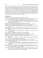
Fig. 1. Isometric (left) and cross-sectional view (right) of an Oxford Instruments ICP-RIE
2.3 Processing Parameters
There are a few important features of an ICP-RIE plasma that have an effect on etching.
Most noticeable during operation is the region of glow discharge, where visible light
emission occurs from a cloud of energetic ions and electrons. As the gas particles move in
the plasma, some collisions occur which transfer energy to bound electrons. When these
electrons return to their ground state, a photon may be emitted. The color of the plasma is
characteristic of the excited gas species, because the photon energy is a function of the
electronic structure of the gas molecules and their interactions with surrounding molecules
(Hodoroaba et al., 2000). This can be a good diagnostic for incorrect plasma striking
conditions or other adverse changes in your plasma. For example, in a multiple gas recipe,
sometimes the emission looks like only one of your gas species, instead of the average of the
colors. This happens when the other species are not being ionized, and thus will cause the
process to take on a completely different character from a calibrated recipe.
Beneath the glow discharge region is a dark space, where atoms are no longer excited into
emitting photons due to the depletion of electrons. This dark space is also the part of the
plasma that most directly affects the paths of incoming ions that will accomplish the etching.
Neutral atoms and other ions will tend to scatter the otherwise straight path of the ions from
the edge of the glow discharge to the cathode.
We can characterize this spreading in both energy and trajectory into probability
distributions, called the ion angular distribution function (IADF) and the ion energy
distribution function (IEDF) (Jansen et al., 2009). These distributions, depicted in Fig. 2,
describe the likelihood that an incident ion has a given energy and trajectory. IADF strongly
affects the sidewall profile, as a wider IADF corresponds to a higher flux of ions reaching
the sidewall. Similarly, the IEDF controls the types of processes the ions can be engaged in
when they reach the surface, including removing passivating species, overcoming activation
energies for chemical reactions, and enhancing sputtering yield. These processes determine
the performance characteristics of an etch, so understanding these effects and recognizing
associated faults are paramount to optimizing a recipe. Parameters controlling the IADF
and IEDF include the bias voltage V
b
, the ion density, the gas composition, and the mean
free path (which also depends on the aforementioned parameters).
++
IEDF
Dark Space
Glow Discharge Region
IADF
Fig. 2. Illustration of the ion angular and ion energy distribution functions, with
hypothetical resultant etched profile distortion. Points in IEDF correspond to different ion
kinetic energies, while points in the IADF correspond to different angles of incidence
2.4 Etch Reaction Dynamics
In wet chemical processes, etching is accomplished through physical dissolution or reaction-
specific dissolution (Reinhardt & Kern, 2008). This takes place at any exposed surface and
thus results in isotropic etching, although the etch rate can vary along different crystalline
orientations due to the bonding state variation of the surfaces. A good example of
crystalline anisotropy in Si wet processing is potassium hydroxide (KOH) etching, which is
widely used for making MEMS structures that capitalize on the direction-dependent etch
rate of KOH (Wolf & Tauber, 2000). However, in a myriad of planar processes that are
utilized in the semiconductor industry, an anisotropic etching profile with sidewalls
perpendicular to the wafer surface is frequently required for effective pattern transfer.
In order to prevent the isotropic or crystalline anisotropic behavior of our processing gases,
the sidewalls must be protected from further etching. This is accomplished by forming a
passivating or inhibiting layer on the sidewall, in one of the following ways:
- Surface passivation
o inserting gases in the plasma which react with wafer materials and
forming involatile compounds (Legtenberg et al., 1995)
o freezing volatile reaction products at the structure’s walls using, e.g.,
cryogenic wafer cooling (Aachboun et al., 2000)
- Inhibitor deposition
o using polymer precursor gases to form physical barrier layers (e.g., C
4
F
8
)
(Kenoyer et al., 2003)
o eroding and redepositing inert mask materials
All of these processes are important to consider when evaluating an etch, as there may be
problems with the etch profile related to the deleterious effect of one of these regimes. We
SemiconductorTechnologies84
use both surface passivation and inhibitor deposition techniques in the following etch
descriptions.
2.5 Time-Dependent Processes
In addition to the previously discussed processing parameters, we have one additional
variable at our disposal: time. A notable example of using time as an etching parameter is
the Bosch silicon etch process, which occurs in a time-multiplexed manner, or “pulsed
mode,” using an etching plasma followed immediately by a deposition plasma.
Alternatively, we can try to accomplish the etching and deposition simultaneously by using
a plasma that contains both etching and deposition gases. This is called a “mixed mode”
process. Finally, we can also tune our processes to change continuously over time in
response to the changing surface condition of our wafer, or to compensate for a negative
effect due to the initial conditions of the wafer.
2.6 Conclusion
As we have seen in this section, plasma processes depend on a large number of variables,
which accounts for both their sensitivity and their flexibility. By having basic knowledge of
the underlying physical processes, diagnosing your processes becomes more intuitive and
makes recipe invention and refinement much easier. In the following sections, we will refer
to many of the concepts covered here to explain results and understand how we arrived at a
given recipe. However, there is still no replacement for hands-on experimentation for
building an even greater understanding of ICP-RIE processing.
3. Deep Silicon Etching
Silicon is the workhorse of the semiconductor industry, and thus etching of Si is one of the
most frequent processes used in a fab. In order to achieve deep etches in silicon using an
ICP-RIE, three basic etch requirements must be met. First, the etch must have a relatively
high etch rate. A slow etch rate is cost prohibitive in a high throughput, industrial process
and has the potential for the introduction of process variations, leading to etch failures.
Second requirement is that the etch must have a high selectivity, or preference, to etch the
silicon as compared to the etch mask. Insufficient selectivity limits the maximum etch depth
or requires complicated thick masks to compensate for erosion, limiting the minimum
feature size. Finally, the etch must remain anisotropic throughout the etching process. If
lateral etching occurs, pattern transfer begins to fail as the etching continues vertically.
To date, only two etching modalities have the potential to stand up to these rigorous
requirements: pulsed mode and mixed mode silicon etches. Both etch schemes employ
forms of etching combined with passivation that actively protect sidewalls during etching
and improve anisotropy. Each has their own advantages and disadvantages which will
become clear during the discussion. To illustrate the differences between the two modes of
etches, two widely used etches will be discussed here. For the pulsed mode etch we
describe the chopping Bosch silicon etch, which uses gas “chopping” to alternately etch and
deposit inhibitor on your surface, and for the mixed mode etch, we demonstrate the
cryogenic silicon etch, which uses a different gas chemistry to form passivating compounds
at the sidewalls at the same time as etching. Note that both gas chemistries reviewed here
can be used in either pulsed or mixed mode.
As mentioned, the chopping Bosch etch requires two alternating plasma steps. The first step
etches the silicon for a short period then rapidly shuts off the gas and plasma. The second
step then initiates a plasma that deposits an inhibitor film on exposed surfaces. This
alternating sequence continues as the etch progresses. Inherent in the discreteness of the
etching is notching on the sidewalls that occurs every step. The duty cycle between steps
controls the etch angle and the total length of the combined steps controls the depth of the
notching.
In contrast, cryogenic silicon etching combines the discrete etch and passivation steps into a
single continuous etch. By using cryogenic temperatures from –80 °C to –140 °C,
improvements in etch mask selectivity and passivation effects are enabled. Both of these
etching chemistries, mask selections, and characteristics will be reviewed here along with
their applications or demonstrations.
3.1 Gas Chemistries
Chopping Bosch etching utilizes sulfur hexafluoride, SF
6
, as the etching gas and
octafluorocyclobutane, C
4
F
8
, as the passivation gas. As described earlier, when the SF
6
is
injected into the chamber, the plasma ionizes and radicalizes the gas molecules to create a
mixture of SF
x
and F
y
ions and neutrals, where x and y range from 0 to 6 and 1 to 2,
respectively (Cliteur et al., 1999). The potential established between the plasma and the
substrate, due in part to the ICP and the CCP power, causes the electric field that drives the
ions down to the substrate. The unmasked silicon then bonds to the fluorine atoms to create
the volatile tetrafluorosilane (SiF
4
) etch product which is then pumped away from the
chamber. The etch becomes a combination of chemical bonding and mechanical milling; the
milling is established from the momentum imparted to the ions from the electric field.
While the chemical etching is essentially isotropic in nature, the mechanical milling is
anisotropic. After a few seconds of etch time, the SF
6
flow is rapidly terminated and the
C
4
F
8
gas is then injected into the chamber for the passivation step. During this step, the C
4
F
8
fragments into smaller CF
x
ions which act as film precursors (Takahashi et al., 2000). A
Teflon-like film forms on the substrate, on both the vertical and horizontal surfaces. The
thickness of the protective layer is dependent on the passivation step time. Once the
deposition is complete and the subsequent etch step begins, the ions first mill away the
horizontal passivation layers and then begin again with the silicon etching. This cyclic
process of etching followed by passivating continues on until the etching is terminated,
leaving the etched silicon structures coated with the passivation polymer.
The cryogenic silicon etch also utilizes the SF
6
chemistry similar to that of the chopping
Bosch. However, by lowering the substrate’s temperature, and by simultaneously injecting
SF
6
and oxygen gas, O
2
, a passivation layer is created simultaneously as the silicon is etched.
The current understanding of the chemical process is that oxygen ions combine with the
fluorine bonded to the silicon surface prior to the silicon’s removal and forms a SiO
x
F
y
layer.
The exact composition of this layer is a topic of current research (Mellhaoui et al., 2005). In a
manner similar to the chopping Bosch passivation, the SiO
x
F
y
passivation layer protects the
exposed vertical silicon while the unmasked horizontal silicon is etched way. To make this
passivation process as energetically favorable as the chemical reaction of making SiF
4
, the
substrate temperature is required to be cooler than approximately –80 °C. When the silicon
AdvancedPlasmaProcessing:Etching,Deposition,
andWaferBondingTechniquesforSemiconductorApplications 85
use both surface passivation and inhibitor deposition techniques in the following etch
descriptions.
2.5 Time-Dependent Processes
In addition to the previously discussed processing parameters, we have one additional
variable at our disposal: time. A notable example of using time as an etching parameter is
the Bosch silicon etch process, which occurs in a time-multiplexed manner, or “pulsed
mode,” using an etching plasma followed immediately by a deposition plasma.
Alternatively, we can try to accomplish the etching and deposition simultaneously by using
a plasma that contains both etching and deposition gases. This is called a “mixed mode”
process. Finally, we can also tune our processes to change continuously over time in
response to the changing surface condition of our wafer, or to compensate for a negative
effect due to the initial conditions of the wafer.
2.6 Conclusion
As we have seen in this section, plasma processes depend on a large number of variables,
which accounts for both their sensitivity and their flexibility. By having basic knowledge of
the underlying physical processes, diagnosing your processes becomes more intuitive and
makes recipe invention and refinement much easier. In the following sections, we will refer
to many of the concepts covered here to explain results and understand how we arrived at a
given recipe. However, there is still no replacement for hands-on experimentation for
building an even greater understanding of ICP-RIE processing.
3. Deep Silicon Etching
Silicon is the workhorse of the semiconductor industry, and thus etching of Si is one of the
most frequent processes used in a fab. In order to achieve deep etches in silicon using an
ICP-RIE, three basic etch requirements must be met. First, the etch must have a relatively
high etch rate. A slow etch rate is cost prohibitive in a high throughput, industrial process
and has the potential for the introduction of process variations, leading to etch failures.
Second requirement is that the etch must have a high selectivity, or preference, to etch the
silicon as compared to the etch mask. Insufficient selectivity limits the maximum etch depth
or requires complicated thick masks to compensate for erosion, limiting the minimum
feature size. Finally, the etch must remain anisotropic throughout the etching process. If
lateral etching occurs, pattern transfer begins to fail as the etching continues vertically.
To date, only two etching modalities have the potential to stand up to these rigorous
requirements: pulsed mode and mixed mode silicon etches. Both etch schemes employ
forms of etching combined with passivation that actively protect sidewalls during etching
and improve anisotropy. Each has their own advantages and disadvantages which will
become clear during the discussion. To illustrate the differences between the two modes of
etches, two widely used etches will be discussed here. For the pulsed mode etch we
describe the chopping Bosch silicon etch, which uses gas “chopping” to alternately etch and
deposit inhibitor on your surface, and for the mixed mode etch, we demonstrate the
cryogenic silicon etch, which uses a different gas chemistry to form passivating compounds
at the sidewalls at the same time as etching. Note that both gas chemistries reviewed here
can be used in either pulsed or mixed mode.
As mentioned, the chopping Bosch etch requires two alternating plasma steps. The first step
etches the silicon for a short period then rapidly shuts off the gas and plasma. The second
step then initiates a plasma that deposits an inhibitor film on exposed surfaces. This
alternating sequence continues as the etch progresses. Inherent in the discreteness of the
etching is notching on the sidewalls that occurs every step. The duty cycle between steps
controls the etch angle and the total length of the combined steps controls the depth of the
notching.
In contrast, cryogenic silicon etching combines the discrete etch and passivation steps into a
single continuous etch. By using cryogenic temperatures from –80 °C to –140 °C,
improvements in etch mask selectivity and passivation effects are enabled. Both of these
etching chemistries, mask selections, and characteristics will be reviewed here along with
their applications or demonstrations.
3.1 Gas Chemistries
Chopping Bosch etching utilizes sulfur hexafluoride, SF
6
, as the etching gas and
octafluorocyclobutane, C
4
F
8
, as the passivation gas. As described earlier, when the SF
6
is
injected into the chamber, the plasma ionizes and radicalizes the gas molecules to create a
mixture of SF
x
and F
y
ions and neutrals, where x and y range from 0 to 6 and 1 to 2,
respectively (Cliteur et al., 1999). The potential established between the plasma and the
substrate, due in part to the ICP and the CCP power, causes the electric field that drives the
ions down to the substrate. The unmasked silicon then bonds to the fluorine atoms to create
the volatile tetrafluorosilane (SiF
4
) etch product which is then pumped away from the
chamber. The etch becomes a combination of chemical bonding and mechanical milling; the
milling is established from the momentum imparted to the ions from the electric field.
While the chemical etching is essentially isotropic in nature, the mechanical milling is
anisotropic. After a few seconds of etch time, the SF
6
flow is rapidly terminated and the
C
4
F
8
gas is then injected into the chamber for the passivation step. During this step, the C
4
F
8
fragments into smaller CF
x
ions which act as film precursors (Takahashi et al., 2000). A
Teflon-like film forms on the substrate, on both the vertical and horizontal surfaces. The
thickness of the protective layer is dependent on the passivation step time. Once the
deposition is complete and the subsequent etch step begins, the ions first mill away the
horizontal passivation layers and then begin again with the silicon etching. This cyclic
process of etching followed by passivating continues on until the etching is terminated,
leaving the etched silicon structures coated with the passivation polymer.
The cryogenic silicon etch also utilizes the SF
6
chemistry similar to that of the chopping
Bosch. However, by lowering the substrate’s temperature, and by simultaneously injecting
SF
6
and oxygen gas, O
2
, a passivation layer is created simultaneously as the silicon is etched.
The current understanding of the chemical process is that oxygen ions combine with the
fluorine bonded to the silicon surface prior to the silicon’s removal and forms a SiO
x
F
y
layer.
The exact composition of this layer is a topic of current research (Mellhaoui et al., 2005). In a
manner similar to the chopping Bosch passivation, the SiO
x
F
y
passivation layer protects the
exposed vertical silicon while the unmasked horizontal silicon is etched way. To make this
passivation process as energetically favorable as the chemical reaction of making SiF
4
, the
substrate temperature is required to be cooler than approximately –80 °C. When the silicon
SemiconductorTechnologies86
is warmed back up to room temperature, the SiO
x
F
y
becomes volatile and leaves the sample
(Pereira et al., 2009).
3.2 Mask Selection
The ultimate test of a mask is the fidelity of pattern transfer into the silicon over the entire
etching period. Since the mask interacts with the etching process parameters, it is vital to
understand which masks to use for different etches. As stated earlier, if the selectivity is too
low a thicker mask is required to achieve the desired etch depths. Furthermore, as the edge
of the mask erodes it will impart undesired slope or features to the sidewalls of the etched
structure, often referred to as mask-induced roughness. For these reasons, deep silicon
etching requires higher selectivity masks. Conventional silicon etch masks are metal,
oxides, and resist.
Metal masks, such as chrome, offer the advantage of high selectivity as high as thousands to
one. This is primarily due to their lack of chemical reactivity with the etch gas molecules
and their mechanical strength. However, metal masks typically induce detrimental effects
such as notching at the top of the etched structures, due to image forces, and unwanted
masking due to redeposited metal introduced by ion sputtering. A particular problem with
chrome during the cryogenic etch is that oxygen radicals appear to be locally deactivated
around the mask reducing the silicon passivation layer near the top of the mask (Jansen et
al., 2009). Silicon dioxide masks typically offer high selectivity (150:1 for Bosch and 200:1 for
cryogenic etching) with the added cost of more complicated patterning. The oxide layer
must be grown or deposited, followed by pattern transfer from another material or resist
into the oxide mask. Increasing the number of processing steps increases the effort needed
for accurate pattern transfer as well as the potential for reduction in mask fidelity. Resist
masks offer the simplicity of a single processing step along with good selectivity
(approximately 75:1 for Bosch and 100:1 for cryogenic etching). These selectivity values
highly depend on process conditions and are seen to widely vary. Jansen et al. have
commented that sidewall protection using resist is better than that using oxide masks due to
the erosion of the resist mask providing additional material to protect the etched walls
(Jansen et al., 2009).
Several new masks have recently demonstrated improvements both in selectivity and in
ease of integration. Sputtered aluminum oxide, or alumina, provides mask selectivity
greater than 5000:1 for cryogenic etching. Because of the extremely high selectivity, only a
thin layer is required for masking. This makes the film easily patterned via resist liftoff,
instead of traditional ion milling for hardmask pattern transfer. Patterning difficulty is only
slightly increased as compared to traditional resist processing. Starting with a photoresist
mask, a thin layer of alumina is sputtered onto the sample. This is followed by liftoff of the
undesired alumina and the resist using acetone. Due the brittle nature of the material, the
alumina cleanly fractures and easily lifts off. Furthermore, since the alumina is electrically
insulating, image force effects and undercutting seen in metal masks are not seen with this
mask. Removal of the alumina mask is easily achieved using buffered hydrofluoric acid or
ammonium hydroxide combined with hydrogen peroxide, both of which do not
significantly etch silicon.
A second new mask innovation is using gallium (Ga) to mask silicon (Chekurov et al., 2009).
The Ga mask is implanted by a focused ion beam (FIB), where a gallium beam is focused on
a silicon sample and writes out the pattern in a similar way to other direct-write lithography
techniques. The dose can be accurately controlled by manipulating the time the beam
spends focused on the silicon as well as the accelerating voltage of the beam. This offers the
advantage of high mask resolution on small feature sizes (~40 nm) without needing a
polymer to be patterned or a developer to be used. Typical dosing creates masks around 30
nm in thickness and offers greater than 1000:1 selectivity in a cryogenic etch. Unfortunately,
mask removal poses a problem since the gallium atoms are implanted in the silicon and
damage to the silicon surface has not yet been characterized. Since using the Ga mask is, in
a sense, a maskless and resistless technique, pattern definition can take place on any surface
upon which the beam can be focused. This presents the opportunity of multidimensional
patterning, such as patterning on a pre-etched sidewall to create a lateral mask.
3.3 Etching Conditions and Optimization
Control over the etch rates, selectivity, sidewall profile, and etch roughness is achieved
through tuning process parameters. The major controllable parameters include ICP power,
forward power, temperature, chamber pressure, and gas flow rates. While this list is not all
inclusive, these parameters directly control the state of the chamber and therefore the
plasma. Many subtleties also play an important role in the etch process. This list would
include silicon loading, chamber conditioning, and chemical interactions in the gas
chemistry and with the mask. Each etch process will have optimization parameters that will
be reactor specific, but this section will assist in building intuition for both the Bosch and the
cryogenic etch.
The ICP power controls the amount of ionization occurring for a given gas flow rate and
chamber pressure. Typically, as the ICP power is increased, the amount of ions created will
also increase. This will increase the chemical etch rate, both vertically and laterally, increase
the milling etch rate, reduce the selectivity by milling the mask away faster, and reduce the
effect of passivation by bombarding the sidewalls more due to the ion angular dispersion
effect. If the vacuum pumping rate does not change, e.g., when controlling the throttle valve
position instead of the chamber pressure, then when increasing the ICP power one can
measure the fact that more gas is ionized by measuring the chamber pressure. It should be
noted that increasing the ICP power does not increase the etch rate infinitely. In fact there is
an optimum ICP power for a given etch gas flow rate. These trends apply for both Bosch
and cryogenic etching for the SF
6
chemistry. Increasing the ICP power for the passivation
step of chopping Bosch, similarly to the etching, will increase the thickness of the
passivation for a given passivation time. A subtle effect of increasing the ICP power is that
it also slightly increases the bias between the plasma and the electrode. For the Bosch etch,
the bias from the forward power is typically much greater in magnitude than plasma
potential increase from the ICP change and the effect is generally unnoticed. Since the
cryogenic etch uses very little forward power, applying more ICP power can significantly
increase the amount of milling occurring. Another subtle effect is that a higher etch rate also
increases the substrate’s temperature. For the cryogenic etch, it is estimated that the
exothermic formation of SiF
4
releases 2 W/cm
2
for an 8
m/min etch rate. For an unmasked
6” Si wafer, this results in approximately 360 W of exothermic heating.
Increasing the forward power establishes a larger electric field between the plasma and the
table electrode. By imparting more momentum to the ions, the silicon milling rate increases.
This usually increases just the vertical etch rate, but due to the IAD (ion angular
distribution) effect the lateral etching does slightly increase. Since the milling action
AdvancedPlasmaProcessing:Etching,Deposition,
andWaferBondingTechniquesforSemiconductorApplications 87
is warmed back up to room temperature, the SiO
x
F
y
becomes volatile and leaves the sample
(Pereira et al., 2009).
3.2 Mask Selection
The ultimate test of a mask is the fidelity of pattern transfer into the silicon over the entire
etching period. Since the mask interacts with the etching process parameters, it is vital to
understand which masks to use for different etches. As stated earlier, if the selectivity is too
low a thicker mask is required to achieve the desired etch depths. Furthermore, as the edge
of the mask erodes it will impart undesired slope or features to the sidewalls of the etched
structure, often referred to as mask-induced roughness. For these reasons, deep silicon
etching requires higher selectivity masks. Conventional silicon etch masks are metal,
oxides, and resist.
Metal masks, such as chrome, offer the advantage of high selectivity as high as thousands to
one. This is primarily due to their lack of chemical reactivity with the etch gas molecules
and their mechanical strength. However, metal masks typically induce detrimental effects
such as notching at the top of the etched structures, due to image forces, and unwanted
masking due to redeposited metal introduced by ion sputtering. A particular problem with
chrome during the cryogenic etch is that oxygen radicals appear to be locally deactivated
around the mask reducing the silicon passivation layer near the top of the mask (Jansen et
al., 2009). Silicon dioxide masks typically offer high selectivity (150:1 for Bosch and 200:1 for
cryogenic etching) with the added cost of more complicated patterning. The oxide layer
must be grown or deposited, followed by pattern transfer from another material or resist
into the oxide mask. Increasing the number of processing steps increases the effort needed
for accurate pattern transfer as well as the potential for reduction in mask fidelity. Resist
masks offer the simplicity of a single processing step along with good selectivity
(approximately 75:1 for Bosch and 100:1 for cryogenic etching). These selectivity values
highly depend on process conditions and are seen to widely vary. Jansen et al. have
commented that sidewall protection using resist is better than that using oxide masks due to
the erosion of the resist mask providing additional material to protect the etched walls
(Jansen et al., 2009).
Several new masks have recently demonstrated improvements both in selectivity and in
ease of integration. Sputtered aluminum oxide, or alumina, provides mask selectivity
greater than 5000:1 for cryogenic etching. Because of the extremely high selectivity, only a
thin layer is required for masking. This makes the film easily patterned via resist liftoff,
instead of traditional ion milling for hardmask pattern transfer. Patterning difficulty is only
slightly increased as compared to traditional resist processing. Starting with a photoresist
mask, a thin layer of alumina is sputtered onto the sample. This is followed by liftoff of the
undesired alumina and the resist using acetone. Due the brittle nature of the material, the
alumina cleanly fractures and easily lifts off. Furthermore, since the alumina is electrically
insulating, image force effects and undercutting seen in metal masks are not seen with this
mask. Removal of the alumina mask is easily achieved using buffered hydrofluoric acid or
ammonium hydroxide combined with hydrogen peroxide, both of which do not
significantly etch silicon.
A second new mask innovation is using gallium (Ga) to mask silicon (Chekurov et al., 2009).
The Ga mask is implanted by a focused ion beam (FIB), where a gallium beam is focused on
a silicon sample and writes out the pattern in a similar way to other direct-write lithography
techniques. The dose can be accurately controlled by manipulating the time the beam
spends focused on the silicon as well as the accelerating voltage of the beam. This offers the
advantage of high mask resolution on small feature sizes (~40 nm) without needing a
polymer to be patterned or a developer to be used. Typical dosing creates masks around 30
nm in thickness and offers greater than 1000:1 selectivity in a cryogenic etch. Unfortunately,
mask removal poses a problem since the gallium atoms are implanted in the silicon and
damage to the silicon surface has not yet been characterized. Since using the Ga mask is, in
a sense, a maskless and resistless technique, pattern definition can take place on any surface
upon which the beam can be focused. This presents the opportunity of multidimensional
patterning, such as patterning on a pre-etched sidewall to create a lateral mask.
3.3 Etching Conditions and Optimization
Control over the etch rates, selectivity, sidewall profile, and etch roughness is achieved
through tuning process parameters. The major controllable parameters include ICP power,
forward power, temperature, chamber pressure, and gas flow rates. While this list is not all
inclusive, these parameters directly control the state of the chamber and therefore the
plasma. Many subtleties also play an important role in the etch process. This list would
include silicon loading, chamber conditioning, and chemical interactions in the gas
chemistry and with the mask. Each etch process will have optimization parameters that will
be reactor specific, but this section will assist in building intuition for both the Bosch and the
cryogenic etch.
The ICP power controls the amount of ionization occurring for a given gas flow rate and
chamber pressure. Typically, as the ICP power is increased, the amount of ions created will
also increase. This will increase the chemical etch rate, both vertically and laterally, increase
the milling etch rate, reduce the selectivity by milling the mask away faster, and reduce the
effect of passivation by bombarding the sidewalls more due to the ion angular dispersion
effect. If the vacuum pumping rate does not change, e.g., when controlling the throttle valve
position instead of the chamber pressure, then when increasing the ICP power one can
measure the fact that more gas is ionized by measuring the chamber pressure. It should be
noted that increasing the ICP power does not increase the etch rate infinitely. In fact there is
an optimum ICP power for a given etch gas flow rate. These trends apply for both Bosch
and cryogenic etching for the SF
6
chemistry. Increasing the ICP power for the passivation
step of chopping Bosch, similarly to the etching, will increase the thickness of the
passivation for a given passivation time. A subtle effect of increasing the ICP power is that
it also slightly increases the bias between the plasma and the electrode. For the Bosch etch,
the bias from the forward power is typically much greater in magnitude than plasma
potential increase from the ICP change and the effect is generally unnoticed. Since the
cryogenic etch uses very little forward power, applying more ICP power can significantly
increase the amount of milling occurring. Another subtle effect is that a higher etch rate also
increases the substrate’s temperature. For the cryogenic etch, it is estimated that the
exothermic formation of SiF
4
releases 2 W/cm
2
for an 8
m/min etch rate. For an unmasked
6” Si wafer, this results in approximately 360 W of exothermic heating.
Increasing the forward power establishes a larger electric field between the plasma and the
table electrode. By imparting more momentum to the ions, the silicon milling rate increases.
This usually increases just the vertical etch rate, but due to the IAD (ion angular
distribution) effect the lateral etching does slightly increase. Since the milling action
SemiconductorTechnologies88
increases, the erosion rate of the mask also increases, thereby reducing the selectivity.
Similar to the temperature effect from increasing ICP power, increasing the forward power
increases the rate and energy of ion bombardment to the substrate. This effect is easily
calculated from the potential difference and the ion flux for the cryogenic etch and is
estimated around 0.5 W/cm
2
.
The Bosch etch is typically insensitive to temperature effects, while the cryogenic etch is
extremely responsive to any temperature changes. Since the Bosch etch is performed at 20
°C, the polymer passivation layer is far from both the melting and freezing regimes.
However, the high temperature dependence of the passivation reaction during the cryogenic
etch means even small temperature fluctuations change the etching profile. Heating by as
little as 5 °C during the cryogenic etch reduces the passivation rate and thereby induces
undercutting due to image force effects. Passivation during the cryogenic etch roughly
begins to occur around –85 °C. However, if the wafer is too cold, SF
x
etch gases and SiF
x
product gases can freeze on the sample sidewalls, adding to the SiO
x
F
y
passivation layer.
Variations in table temperature by 5 °C due to oscillations in the table temperature
controller have been seen to change the profile of deep etches adding a sinusoidal curvature
to the sidewalls. Temperature is typically controlled by cooling the stage with liquid
nitrogen or water and thermally connecting the wafer to the table by flowing helium
between them. When silicon samples smaller than a full wafer are etched, they require
thermal conductivity to the carrier wafer. This is accomplished by using thermal grease or
Fomblin pump oil on the backside of the wafer to the substrate. Removal of the thermal
grease is done with trichloroethylene and the Fomblin is easily removed by isopropanol.
Chamber pressure controls the amount of gas in the chamber for ionization. As noted
during the ICP power discussion, changing the amount of incident ions controls both etch
rate and selectivity. For a given ICP power, there is an optimum gas flow rate for SF
6
.
Increasing the pressure can be accomplished by shutting the throttle valve or by injecting
more gas. A subtle effect of increasing chamber pressure is that it also increases the
scattering collisions of ions traversing the Faraday dark space. This creates a larger angular
spread in incident ions to the substrate, or increases the IAD. This increases the amount of
undercut or lateral etch.
Other parameters which can alter both the Bosch and the cryogenic etch are not necessarily
due to changing a mechanical feature on the reactor. Changing the amount of exposed
silicon can also change etch results. Increasing the ratio of exposed silicon to masked silicon
changes the amount of ions needed for etching and will significantly reduce the etch rate.
As explained earlier, the exothermic nature of etching more silicon also induces an increase
in substrate heating. A positive effect, however, is that for large silicon loading, slight
changes in mask patterning have relatively minor effects in etch results. This is a convenient
feature for establishing an etch for a wide range of users. It also reduces the effect of
changing the etch as the etch goes deeper into the silicon and effectively exposes more
silicon surface. Cleanliness of the chamber can also change the effects of etches. Since the
plasma interacts with the sidewalls as well as the substrate, residual molecules on the
sidewalls can be redeposited on the etched surface, causing micromasking, or can
chemically react with the etch gas. For this reason, it is highly recommended that good
chamber cleans followed by chamber conditioning be performed prior to etching.
3.4 Application: High Aspect Ratio Pillars and Metallization Liftoff
Using the high selectivity of photoresist for the cryogenic silicon etch, fabrication of high
aspect ratio micropillars was demonstrated (Henry et al., 2009a) and serves as an example of
achievable profiles using the mixed mode etching process. These pillars were utilized for
validating theories concerning radial p–n junctions for applications of solar cells (Kayes et
al., 2008). The patterns transferred to a 1.6
m thick photoresist on a silicon substrate were
groups of disks 5, 10, 20, and 50
m in diameter in a hexagonal array. The spacing between
each disk grouping was equivalent to the diameter of the disks, i.e., each 5
m disk was
separated from its nearest neighbor by 5
m, the 10
m disks by 10
m, etc.
Fig. 3. High aspect ratio silicon micropillars: This cross-sectional SEM of 5
m wide and 83
m tall silicon micropillars demonstrates the cryogenic silicon etch using a 110 nm thick
alumina etch mask. The very tops of the pillars indicate that mask erosion is beginning
Concluding etch profile optimization, multiple samples of the patterns were etched for
varying times. Since each etch had an array of the four different diameters, a direct study of
aspect ratio, i.e., ratio of the etched depth to width, dependence upon etch depth was made.
Assuming that the etch rate was comprised of the etch rate of silicon with no structures
(zero aspect ratio) minus a linear dependence on aspect ratio, a simple differential equation
may be solved to yield the following:
AdvancedPlasmaProcessing:Etching,Deposition,
andWaferBondingTechniquesforSemiconductorApplications 89
increases, the erosion rate of the mask also increases, thereby reducing the selectivity.
Similar to the temperature effect from increasing ICP power, increasing the forward power
increases the rate and energy of ion bombardment to the substrate. This effect is easily
calculated from the potential difference and the ion flux for the cryogenic etch and is
estimated around 0.5 W/cm
2
.
The Bosch etch is typically insensitive to temperature effects, while the cryogenic etch is
extremely responsive to any temperature changes. Since the Bosch etch is performed at 20
°C, the polymer passivation layer is far from both the melting and freezing regimes.
However, the high temperature dependence of the passivation reaction during the cryogenic
etch means even small temperature fluctuations change the etching profile. Heating by as
little as 5 °C during the cryogenic etch reduces the passivation rate and thereby induces
undercutting due to image force effects. Passivation during the cryogenic etch roughly
begins to occur around –85 °C. However, if the wafer is too cold, SF
x
etch gases and SiF
x
product gases can freeze on the sample sidewalls, adding to the SiO
x
F
y
passivation layer.
Variations in table temperature by 5 °C due to oscillations in the table temperature
controller have been seen to change the profile of deep etches adding a sinusoidal curvature
to the sidewalls. Temperature is typically controlled by cooling the stage with liquid
nitrogen or water and thermally connecting the wafer to the table by flowing helium
between them. When silicon samples smaller than a full wafer are etched, they require
thermal conductivity to the carrier wafer. This is accomplished by using thermal grease or
Fomblin pump oil on the backside of the wafer to the substrate. Removal of the thermal
grease is done with trichloroethylene and the Fomblin is easily removed by isopropanol.
Chamber pressure controls the amount of gas in the chamber for ionization. As noted
during the ICP power discussion, changing the amount of incident ions controls both etch
rate and selectivity. For a given ICP power, there is an optimum gas flow rate for SF
6
.
Increasing the pressure can be accomplished by shutting the throttle valve or by injecting
more gas. A subtle effect of increasing chamber pressure is that it also increases the
scattering collisions of ions traversing the Faraday dark space. This creates a larger angular
spread in incident ions to the substrate, or increases the IAD. This increases the amount of
undercut or lateral etch.
Other parameters which can alter both the Bosch and the cryogenic etch are not necessarily
due to changing a mechanical feature on the reactor. Changing the amount of exposed
silicon can also change etch results. Increasing the ratio of exposed silicon to masked silicon
changes the amount of ions needed for etching and will significantly reduce the etch rate.
As explained earlier, the exothermic nature of etching more silicon also induces an increase
in substrate heating. A positive effect, however, is that for large silicon loading, slight
changes in mask patterning have relatively minor effects in etch results. This is a convenient
feature for establishing an etch for a wide range of users. It also reduces the effect of
changing the etch as the etch goes deeper into the silicon and effectively exposes more
silicon surface. Cleanliness of the chamber can also change the effects of etches. Since the
plasma interacts with the sidewalls as well as the substrate, residual molecules on the
sidewalls can be redeposited on the etched surface, causing micromasking, or can
chemically react with the etch gas. For this reason, it is highly recommended that good
chamber cleans followed by chamber conditioning be performed prior to etching.
3.4 Application: High Aspect Ratio Pillars and Metallization Liftoff
Using the high selectivity of photoresist for the cryogenic silicon etch, fabrication of high
aspect ratio micropillars was demonstrated (Henry et al., 2009a) and serves as an example of
achievable profiles using the mixed mode etching process. These pillars were utilized for
validating theories concerning radial p–n junctions for applications of solar cells (Kayes et
al., 2008). The patterns transferred to a 1.6
m thick photoresist on a silicon substrate were
groups of disks 5, 10, 20, and 50
m in diameter in a hexagonal array. The spacing between
each disk grouping was equivalent to the diameter of the disks, i.e., each 5
m disk was
separated from its nearest neighbor by 5
m, the 10
m disks by 10
m, etc.
Fig. 3. High aspect ratio silicon micropillars: This cross-sectional SEM of 5
m wide and 83
m tall silicon micropillars demonstrates the cryogenic silicon etch using a 110 nm thick
alumina etch mask. The very tops of the pillars indicate that mask erosion is beginning
Concluding etch profile optimization, multiple samples of the patterns were etched for
varying times. Since each etch had an array of the four different diameters, a direct study of
aspect ratio, i.e., ratio of the etched depth to width, dependence upon etch depth was made.
Assuming that the etch rate was comprised of the etch rate of silicon with no structures
(zero aspect ratio) minus a linear dependence on aspect ratio, a simple differential equation
may be solved to yield the following:
SemiconductorTechnologies90
0
( ) 1 exp .
E w
bt
d t
b w
Here E
0
and b are the zero aspect ratio etch rate and the aspect ratio dependent etch rate,
respectively. The equation solves for the etch depth d given the etched trench width w and
the etching time t. Using this equation, etches were performed achieving an aspect ratio of
17.5:1. The angle of the micropillars’ sidewalls was controlled by varying the oxygen flow
rate, which allowed for passivation rates to be controlled and consequently changing the
angle of the profile up to 6°. This number appears small at first but when deep etches are
being performed, controlling the angle can prove critical to not etching the base of the pillars
to a point.
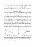
Fig. 4. Etch rates and aspect ratio dependence: This graph contains data points taken from
etches creating the silicon micropillar arrays of 5, 10, 20, and 50
m diameter pillars as well
as the solutions to the solved differential equation for the various widths. It becomes
evident that as the aspect ratio of the etched trench increases, the etch rate slows down. This
is the so-called “Aspect Ratio Dependent Etching” or ARDE effect
A second use of the cryogenic etch is based on the high selectivity of the etch mask. Since
very little resist is eroded away during etching, the remaining etch mask becomes useful as a
layer for metallization liftoff. This fabrication sequence was employed for creating silicon
microcoils (Henry et al., 2009b). Using a 1.6
m thick patterned photoresist, a cryogenic etch
was used to etch highly doped silicon. The structures then had varying thicknesses of
chemically vapor deposited (CVD) amorphous silicon dioxide. Following the deposition,
copper was thermally evaporated into the trenches with thickness up to 15
m. Liftoff of the
silicon dioxide and metal using acetone was then performed. Typically for conventional
metallization, resist heights are required to be 3–4 times thicker than the metal being
deposited with necessary rigorous sidewall profile control. Here, since the metal is
approximately 10 times thicker than the resist, the depth of the cryogenic etch can replace
the thick resist requirements as well as reliably accomplishing the profile requirements
needed for the thick metal deposit. This fabrication sequence created planar copper
microcoils embedded in silicon and insulated from the substrate using silicon dioxide.
Fig. 5. Planar copper microcoils in cross section. Coils are copper 10
m thick embedded in
silicon and insulated using a 1
m thick CVD oxide. Using the high selectivity of the
cryogenic silicon etch, thick copper metallization is possible with liftoff achieved using the
etch mask
4. Nanoscale Silicon Etching
Unlike deep silicon etching, nanoscale etching requires neither extraordinary selectivity nor
large etch rates. On the contrary, moderate selectivity of 5:1 is acceptable and slower etch
rates, 100–200 nm/min, are more useful for accuracy of etch depths. Further, Bosch etching
and cryogenic etching prove to be unsuitable for very small structures due to the notching
and lateral etching of the two chemistries respectively. In general, nanoscale etch properties
should include smooth and highly controllable sidewalls, slow etch rates, and low
undercutting effects. To meet the first two requirements, mixed mode gas chemistries
become useful due to the simultaneous etching and passivating. Proper choices in masks
can reduce undercutting effects. This section will discuss several emerging mask
AdvancedPlasmaProcessing:Etching,Deposition,
andWaferBondingTechniquesforSemiconductorApplications 91
0
( ) 1 exp .
E w
bt
d t
b w
Here E
0
and b are the zero aspect ratio etch rate and the aspect ratio dependent etch rate,
respectively. The equation solves for the etch depth d given the etched trench width w and
the etching time t. Using this equation, etches were performed achieving an aspect ratio of
17.5:1. The angle of the micropillars’ sidewalls was controlled by varying the oxygen flow
rate, which allowed for passivation rates to be controlled and consequently changing the
angle of the profile up to 6°. This number appears small at first but when deep etches are
being performed, controlling the angle can prove critical to not etching the base of the pillars
to a point.
Fig. 4. Etch rates and aspect ratio dependence: This graph contains data points taken from
etches creating the silicon micropillar arrays of 5, 10, 20, and 50
m diameter pillars as well
as the solutions to the solved differential equation for the various widths. It becomes
evident that as the aspect ratio of the etched trench increases, the etch rate slows down. This
is the so-called “Aspect Ratio Dependent Etching” or ARDE effect
A second use of the cryogenic etch is based on the high selectivity of the etch mask. Since
very little resist is eroded away during etching, the remaining etch mask becomes useful as a
layer for metallization liftoff. This fabrication sequence was employed for creating silicon
microcoils (Henry et al., 2009b). Using a 1.6
m thick patterned photoresist, a cryogenic etch
was used to etch highly doped silicon. The structures then had varying thicknesses of
chemically vapor deposited (CVD) amorphous silicon dioxide. Following the deposition,
copper was thermally evaporated into the trenches with thickness up to 15
m. Liftoff of the
silicon dioxide and metal using acetone was then performed. Typically for conventional
metallization, resist heights are required to be 3–4 times thicker than the metal being
deposited with necessary rigorous sidewall profile control. Here, since the metal is
approximately 10 times thicker than the resist, the depth of the cryogenic etch can replace
the thick resist requirements as well as reliably accomplishing the profile requirements
needed for the thick metal deposit. This fabrication sequence created planar copper
microcoils embedded in silicon and insulated from the substrate using silicon dioxide.
Fig. 5. Planar copper microcoils in cross section. Coils are copper 10
m thick embedded in
silicon and insulated using a 1
m thick CVD oxide. Using the high selectivity of the
cryogenic silicon etch, thick copper metallization is possible with liftoff achieved using the
etch mask
4. Nanoscale Silicon Etching
Unlike deep silicon etching, nanoscale etching requires neither extraordinary selectivity nor
large etch rates. On the contrary, moderate selectivity of 5:1 is acceptable and slower etch
rates, 100–200 nm/min, are more useful for accuracy of etch depths. Further, Bosch etching
and cryogenic etching prove to be unsuitable for very small structures due to the notching
and lateral etching of the two chemistries respectively. In general, nanoscale etch properties
should include smooth and highly controllable sidewalls, slow etch rates, and low
undercutting effects. To meet the first two requirements, mixed mode gas chemistries
become useful due to the simultaneous etching and passivating. Proper choices in masks
can reduce undercutting effects. This section will discuss several emerging mask
SemiconductorTechnologies92
technologies and demonstrate nanoscale etching using SF
6
/C
4
F
8
, termed as the Pseudo
Bosch etch here.
4.1 Gas Chemistries
Although the cryogenic etch creates very smooth sidewalls, its inherent undercut is typically
too much for the nanoscale regime. Furthermore, the etch rates are too high for accurate
control on the nanoscale. A combination of the Bosch gases introduced in a mixed mode
process creates an ideal etch recipe which has allowed silicon nanopillars with an aspect
ratio of 60:1 and diameters down to 20 nm. To etch the silicon, SF
6
is again used while C
4
F
8
is used to passivate simultaneously. Since ions are constantly needing to mill the
continuously deposited fluorocarbon polymer layer, the etch rate significantly reduces to
200–300 nm/min. Etch recipe parameters are similar to the cryogenic etch and are around
1200 W for the ICP power and 20 W for the forward power. The advantage of using the C
4
F
8
as the passivation gas also extends to not requiring cryogenic temperatures.
4.2 Mask Selection
Typical masks for nanoscale etches are based on the difficult patterning requirements. To
define structures down to 20 nm, e-beam resists such as polymethylmethacrylate (PMMA)
are employed with thicknesses ranging from 500 nm down to 30 nm. The advantage of
using this as the etch mask is the simplicity in pattern transfer: once the e-beam patterning is
complete, the resist can be developed leaving the patterned etch mask. The disadvantage is
that typical selectivity values range from 4:1 to 0.5:1. This implies that only very shallow
etches can be performed on the very small structures since thicker e-beam resists are
difficult to expose for small structures. However, a great advantage is achieved by using
alumina etch masks with this etch. A thin layer of alumina, approximately 30 nm thick, can
serve as an etch mask yielding selectivity of better than 60:1. This allows for e-beam resists,
with thickness to be patterned and developed, followed by having the alumina sputter
deposited. After liftoff in acetone, the alumina pattern remains on the silicon. Another
common etch mask is nickel, which is patterned similarly to that of sputtered alumina.
Sputtered nickel offers good selectivity with the disadvantage of increased mask
undercutting due to image forces.
We recently have also demonstrated using implanted gallium as an etch mask for silicon
nanostructures. With this method, Ga ions are implanted in the silicon substrate using a
focused ion beam. The dwell time of the beam combined with the current determines the
dosage while the beam accelerating voltage determines the depth and spread of the mask.
Typical threshold dosages are about 10
16
ions/cm
2
or 2000
C/cm
2
. For comparison, typical
resist sensitivities range from 200–1200
C/cm
2
when exposed on a 100 keV electron beam
lithography system. Using a 30 kV beam, we estimate the Ga layer to be approximately 20
nm thick. Using the Pseudo Bosch etch, selectivities greater than 50:1 have been
demonstrated using a Ga mask with resolution of better than 60 nm. At this point, we
suspect that the resolution has not reached the intrinsic limit imposed by the implantation
process, and is instead limited by our beam optics.
Fig. 6. Ga etch mask for Pseudo Bosch etch: This cross-sectional SEM, taken at 45°, of a
series of blocks etched to 700 nm demonstrates focused ion beam implanted Ga acting as an
etch mask for the Pseudo Bosch etch. The smallest resolvable feature here is 80 nm;
however mask erosion did occur for the 2×10
16
ions/cm
2
Ga dose. The simulated Ga
implantation depth is 27 nm with a longitudinal spread of 9 nm
4.3 Etching Conditions and Optimization
By changing the ratio of the etch gas to passivation gas, SF
6
:C
4
F
8
, the sidewall profile can be
controlled. A typical ratio is 1:3 with the absolute gas flow rates dependent upon chamber
volume, as sufficient flow is required to establish a chamber pressure of 10 mTorr; a good
starting point is roughly 30 and 90 sccm respectively. Increasing the ratio improves the etch
rate, reduces the selectivity, and drives the sidewall to be reentrant. Typical ICP power is
around 1200 W combined with a slightly higher forward power than that of the cryogenic
etch of around 20 W. Increasing the forward power again reduces the selectivity with a
slight improvement in etching rates. Unlike cryogenic mixed mode, this etch is typically
performed at room temperature or 15–20 °C.
4.4 Application: Waveguides and Nanopillars
Since passivation occurs during etching, very straight and smooth sidewalls can be
fabricated on nanoscale structures. In particular, combining this feature of the Pseudo Bosch
etch with the high selectivity of the alumina etch mask, impressive 60:1 aspect ratio
nanopillars have been demonstrated. Pillars were created by first patterning PMMA using a
100 kV electron beam and developing the pattern using methyl isobutyl ketone (MIBK) and
isopropanol solution. A 30 nm thick alumina layer was then sputtered and lifted off leaving
the alumina mask on silicon. The Pseudo Bosch etch was then performed with an etch rate
of 250 nm/min leaving well defined arrays of silicon nanopillars. The smallest diameter
created was 22 nm for a pillar standing 1.26
m tall.
AdvancedPlasmaProcessing:Etching,Deposition,
andWaferBondingTechniquesforSemiconductorApplications 93
technologies and demonstrate nanoscale etching using SF
6
/C
4
F
8
, termed as the Pseudo
Bosch etch here.
4.1 Gas Chemistries
Although the cryogenic etch creates very smooth sidewalls, its inherent undercut is typically
too much for the nanoscale regime. Furthermore, the etch rates are too high for accurate
control on the nanoscale. A combination of the Bosch gases introduced in a mixed mode
process creates an ideal etch recipe which has allowed silicon nanopillars with an aspect
ratio of 60:1 and diameters down to 20 nm. To etch the silicon, SF
6
is again used while C
4
F
8
is used to passivate simultaneously. Since ions are constantly needing to mill the
continuously deposited fluorocarbon polymer layer, the etch rate significantly reduces to
200–300 nm/min. Etch recipe parameters are similar to the cryogenic etch and are around
1200 W for the ICP power and 20 W for the forward power. The advantage of using the C
4
F
8
as the passivation gas also extends to not requiring cryogenic temperatures.
4.2 Mask Selection
Typical masks for nanoscale etches are based on the difficult patterning requirements. To
define structures down to 20 nm, e-beam resists such as polymethylmethacrylate (PMMA)
are employed with thicknesses ranging from 500 nm down to 30 nm. The advantage of
using this as the etch mask is the simplicity in pattern transfer: once the e-beam patterning is
complete, the resist can be developed leaving the patterned etch mask. The disadvantage is
that typical selectivity values range from 4:1 to 0.5:1. This implies that only very shallow
etches can be performed on the very small structures since thicker e-beam resists are
difficult to expose for small structures. However, a great advantage is achieved by using
alumina etch masks with this etch. A thin layer of alumina, approximately 30 nm thick, can
serve as an etch mask yielding selectivity of better than 60:1. This allows for e-beam resists,
with thickness to be patterned and developed, followed by having the alumina sputter
deposited. After liftoff in acetone, the alumina pattern remains on the silicon. Another
common etch mask is nickel, which is patterned similarly to that of sputtered alumina.
Sputtered nickel offers good selectivity with the disadvantage of increased mask
undercutting due to image forces.
We recently have also demonstrated using implanted gallium as an etch mask for silicon
nanostructures. With this method, Ga ions are implanted in the silicon substrate using a
focused ion beam. The dwell time of the beam combined with the current determines the
dosage while the beam accelerating voltage determines the depth and spread of the mask.
Typical threshold dosages are about 10
16
ions/cm
2
or 2000
C/cm
2
. For comparison, typical
resist sensitivities range from 200–1200
C/cm
2
when exposed on a 100 keV electron beam
lithography system. Using a 30 kV beam, we estimate the Ga layer to be approximately 20
nm thick. Using the Pseudo Bosch etch, selectivities greater than 50:1 have been
demonstrated using a Ga mask with resolution of better than 60 nm. At this point, we
suspect that the resolution has not reached the intrinsic limit imposed by the implantation
process, and is instead limited by our beam optics.
Fig. 6. Ga etch mask for Pseudo Bosch etch: This cross-sectional SEM, taken at 45°, of a
series of blocks etched to 700 nm demonstrates focused ion beam implanted Ga acting as an
etch mask for the Pseudo Bosch etch. The smallest resolvable feature here is 80 nm;
however mask erosion did occur for the 2×10
16
ions/cm
2
Ga dose. The simulated Ga
implantation depth is 27 nm with a longitudinal spread of 9 nm
4.3 Etching Conditions and Optimization
By changing the ratio of the etch gas to passivation gas, SF
6
:C
4
F
8
, the sidewall profile can be
controlled. A typical ratio is 1:3 with the absolute gas flow rates dependent upon chamber
volume, as sufficient flow is required to establish a chamber pressure of 10 mTorr; a good
starting point is roughly 30 and 90 sccm respectively. Increasing the ratio improves the etch
rate, reduces the selectivity, and drives the sidewall to be reentrant. Typical ICP power is
around 1200 W combined with a slightly higher forward power than that of the cryogenic
etch of around 20 W. Increasing the forward power again reduces the selectivity with a
slight improvement in etching rates. Unlike cryogenic mixed mode, this etch is typically
performed at room temperature or 15–20 °C.
4.4 Application: Waveguides and Nanopillars
Since passivation occurs during etching, very straight and smooth sidewalls can be
fabricated on nanoscale structures. In particular, combining this feature of the Pseudo Bosch
etch with the high selectivity of the alumina etch mask, impressive 60:1 aspect ratio
nanopillars have been demonstrated. Pillars were created by first patterning PMMA using a
100 kV electron beam and developing the pattern using methyl isobutyl ketone (MIBK) and
isopropanol solution. A 30 nm thick alumina layer was then sputtered and lifted off leaving
the alumina mask on silicon. The Pseudo Bosch etch was then performed with an etch rate
of 250 nm/min leaving well defined arrays of silicon nanopillars. The smallest diameter
created was 22 nm for a pillar standing 1.26
m tall.
SemiconductorTechnologies94
Fig. 7. High aspect ratio silicon nanopillars: These cross-sectional SEMs, taken at 45°, of a)
73 nm diameter and 2.8
m tall silicon nanopillar, b) 40 nm diameter and 1.75
m tall silicon
nanopillar, c) tungsten probe contacting a 200 nm diameter and 1.25
m tall silicon
nanopillar, and d) array of alternating 40 nm and 65 nm diameter pillars 1
m tall
demonstrate the Pseudo Bosch silicon etch using a 30 nm thick alumina etch mask
5. Nanoscale Indium Phosphide Etching
In contrast to the previously discussed fluorine-based etch recipes, many III–V materials
require the use of chlorine-based chemistries. This is due to the difference in chemical
properties of the etch products. As seen in the previous section, the proposed mechanism
for Ga masking of Si is the formation of involatile GaF
x
compounds that prevent further
etching. Thus, for etching of Ga and other similar compounds, we expect that a Cl
2
-based
etch will result in faster etching rate and smoother sidewalls from the readily removed etch
products. In this section, we will discuss an InP etch that uses a hybrid gas mixture of Cl
2
,
CH
4
, and H
2
.
5.1 Gas Chemistries
The gas composition of this etching recipe is a hybrid between two established InP recipes.
Specifically, high etch rate recipes with Cl
2
- and Cl
2
/Ar-based plasmas are well known but
suffer from sidewall roughness and require high processing temperatures to volatilize InCl
x
species (Yu & Lee, 2002), as illustrated in Fig. 8. Smooth etch recipes with CH
4
/H
2
plasmas
have also been studied but have prohibitively slow etch rates. In this case, the smoothness
is a result of two factors. Firstly, the likely etching mechanism of InP is the evolution of
volatile products PH
3
and In(CH
3
)
3
, which can be controlled by adjusting the gas flow rates
(Feurprier et al., 1998). Secondly, the deposition of CH films from the source gases serves to
protect the sidewalls (von Keudell & Möller, 1994). In our etch, we utilize a precise ratio of
source gases that balances all these properties and takes interactions into account, such as
removal of H and Cl ions by formation of HCl.
Fig. 8. Micromasking due to insufficient heating (left). By increasing ICP power and thus
raising sample temperature, micromasking is removed (right)
5.2 Mask Selection
Appropriate masks for the InP etch are metals and dielectrics. This is due to the high rate of
mask erosion inherent in the etching conditions. The forward bias and thus bias voltage
that drive ions toward the wafer surface are much higher than those found in the SF
6
-based
silicon etches in previous sections. This will make the etch more milling, and will help to
maintain the same etch characteristics in other stoichiometries of interest, such as InGaAsP
compounds. We utilized masks of silicon dioxide spheres and evaporated Au layers in the
etching experiments. The selectivity of oxide was approximately 10:1; however, faceting
occurred before the mask was completely eroded, limiting the useful selectivity to a more
modest 4:1. In deeper nanoscale etching applications, a silicon nitride or metal mask is
preferred as it has high selectivity and does not suffer from faceting as readily as oxide. As
seen in Fig. 9, the metal hardmask has eliminated most pattern-induced roughness.
Fig. 9. Anisotropic InP etch using a metal hardmask. Smoothness is only limited by mask
irregularities
AdvancedPlasmaProcessing:Etching,Deposition,
andWaferBondingTechniquesforSemiconductorApplications 95
Fig. 7. High aspect ratio silicon nanopillars: These cross-sectional SEMs, taken at 45°, of a)
73 nm diameter and 2.8
m tall silicon nanopillar, b) 40 nm diameter and 1.75
m tall silicon
nanopillar, c) tungsten probe contacting a 200 nm diameter and 1.25
m tall silicon
nanopillar, and d) array of alternating 40 nm and 65 nm diameter pillars 1
m tall
demonstrate the Pseudo Bosch silicon etch using a 30 nm thick alumina etch mask
5. Nanoscale Indium Phosphide Etching
In contrast to the previously discussed fluorine-based etch recipes, many III–V materials
require the use of chlorine-based chemistries. This is due to the difference in chemical
properties of the etch products. As seen in the previous section, the proposed mechanism
for Ga masking of Si is the formation of involatile GaF
x
compounds that prevent further
etching. Thus, for etching of Ga and other similar compounds, we expect that a Cl
2
-based
etch will result in faster etching rate and smoother sidewalls from the readily removed etch
products. In this section, we will discuss an InP etch that uses a hybrid gas mixture of Cl
2
,
CH
4
, and H
2
.
5.1 Gas Chemistries
The gas composition of this etching recipe is a hybrid between two established InP recipes.
Specifically, high etch rate recipes with Cl
2
- and Cl
2
/Ar-based plasmas are well known but
suffer from sidewall roughness and require high processing temperatures to volatilize InCl
x
species (Yu & Lee, 2002), as illustrated in Fig. 8. Smooth etch recipes with CH
4
/H
2
plasmas
have also been studied but have prohibitively slow etch rates. In this case, the smoothness
is a result of two factors. Firstly, the likely etching mechanism of InP is the evolution of
volatile products PH
3
and In(CH
3
)
3
, which can be controlled by adjusting the gas flow rates
(Feurprier et al., 1998). Secondly, the deposition of CH films from the source gases serves to
protect the sidewalls (von Keudell & Möller, 1994). In our etch, we utilize a precise ratio of
source gases that balances all these properties and takes interactions into account, such as
removal of H and Cl ions by formation of HCl.
Fig. 8. Micromasking due to insufficient heating (left). By increasing ICP power and thus
raising sample temperature, micromasking is removed (right)
5.2 Mask Selection
Appropriate masks for the InP etch are metals and dielectrics. This is due to the high rate of
mask erosion inherent in the etching conditions. The forward bias and thus bias voltage
that drive ions toward the wafer surface are much higher than those found in the SF
6
-based
silicon etches in previous sections. This will make the etch more milling, and will help to
maintain the same etch characteristics in other stoichiometries of interest, such as InGaAsP
compounds. We utilized masks of silicon dioxide spheres and evaporated Au layers in the
etching experiments. The selectivity of oxide was approximately 10:1; however, faceting
occurred before the mask was completely eroded, limiting the useful selectivity to a more
modest 4:1. In deeper nanoscale etching applications, a silicon nitride or metal mask is
preferred as it has high selectivity and does not suffer from faceting as readily as oxide. As
seen in Fig. 9, the metal hardmask has eliminated most pattern-induced roughness.
Fig. 9. Anisotropic InP etch using a metal hardmask. Smoothness is only limited by mask
irregularities
SemiconductorTechnologies96
5.3 Etching Conditions and Optimization
Our etch had Cl
2
:H
2
:CH
4
ratio of 8:7:4 with actual gas flows of 32 sccm Cl
2
, 28 sccm H
2
, and
16 sccm CH
4
and a chamber pressure of 4 mTorr. The table was heated to 60 °C to reduce
polymer deposition, and no helium backing was applied in order to have the plasma heat
the sample. This heating is key to proper etch characteristics, as too little heat will cause
micromasking due to involatile gas products such as InCl
x
. The forward power was 180 W,
found experimentally by varying until an anisotropic profile was achieved without
excessive mask erosion. This resulted in a cathode bias of approximately 200 V. ICP power
was 2200 W, also found experimentally by monitoring the transition of “black” InP to
smooth InP due to the cessation of micromasking during etching. The etch rate of pure InP
was measured to be 1.2
m/min.
Fig. 10. InGaAsP on InP etching showing excessive forward power (left) and the correct
amount of forward power (right). The features at the bottom of the pillar are due to faceting
and redeposition of mask materials
During some etches with identical conditions, a roughening of the bottom surface was
noticed due to chamber cleanliness. The sensitivity of this etch to chamber condition is not
as high as the cryogenic Si etch described earlier, but reproducible results require a regular
cleaning schedule to return the chamber to a known “clean” state. This is best implemented
by running a short, minute-long SF
6
cleaning plasma just before etching to remove any
contaminants that are readily incorporated into the plasma. For long term cleanliness,
periodic hour-long SF
6
/O
2
plasma is run. The frequency depends on what other etches have
been performed previously, but is typically one hour of cleaning per three to four hours of
etching. In an industrial setting, this could be done in shorter periods between each wafer to
maintain a constant chamber state.
6. Inductively Coupled Plasma Chemical Vapor Deposition
ICP-RIE systems have been demonstrated in this chapter to be a gentle environment for
etching both silicon and III–V materials. Over the last decade, research has extended this
useful environment to the deposition of thin dielectric films and conductive silicon layers.
A common film deposition method is low pressure chemical vapor deposition, which is
typically performed at temperatures around 600 °C. The low pressure limits unwanted gas
phase reactions, while the high temperature ensures that there are adequate diffusion and
energy to overcome any activation barrier in the desired reactions. By using plasma
enhanced chemical vapor deposition (PECVD), typical deposition temperature can be
lowered to the range of 300 °C to 400 °C. By adding a gas ring to improve gas uniformity in
an ICP-RIE, the new operation of ICP chemical vapor deposition, or ICP-CVD, is added to
the machine. In ICP-CVD, depositions may proceed with temperatures in the range of 50 °C
to 150 °C. Densities of layers deposited at 70 °C using ICP-CVD have now become
comparable to PECVD at 350 °C. This illustrates the key advantage of ICP-CVD over
traditional CVD processes: high density films deposited at lower temperatures.
A typical PECVD reactor has a single power source establishing both the plasma density
and the ion flux in a method similar to that of an RIE (although new PECVD reactors can
have a 13.56 MHz source combined with a kHz source, where both of the sources create RIE
plasmas albeit at different frequencies). A unique advantage of ICP-CVD reactors over
PECVD is that both the ion density and the ion flux can be independently controlled. In this
case, the ICP power changes the ion density while the forward power controls the ion flux
(Lee et al., 2000). This provides another method for tuning film parameters such as optical
index, deposition rate, and density.
Since the ICP-RIE has improved efficiency ionizing the gas over an RIE-only reactor, and
due to the lower operating pressures of ICP-RIEs over that of PECVD, significantly less gas
is required for depositions. Typical flow rates for gases are 20 to 100 sccm. However,
typical deposition rates for ICP-CVD are significantly lower than PECVD, ranging from 6–
30 nm/min whereas PECVD rates range from 60–250 nm/min. The slower rates in the ICP-
CVD allow for precise control over thin films with the intended use as dielectrics. Using the
same method for creation of thicker films for etch masks becomes impractical.
6.1 Gas Chemistries
Types of films available using ICP-CVD include SiO
2
, SiN
x
, SiON
x
, a-Si, and SiC. All of
these silicon containing compounds require the source gas silane (SiH
4
). Because silane is
pyrophoric and will combust spontaneously in air, it is typically diluted to 2–10% levels
using inert carrier gases such as nitrogen, helium, or argon. The silane flows into the reactor
through a gas ring surrounding the table. A second gas is injected from the top of the
chamber where the ICP ionizes the gas, creating various radicals and ions. In the same
manner as in etching processes, the electrostatic potential difference between the plasma
and the table drives the ions to the wafer surface, where they chemically combine with
silane to create the film. Typical additive gases are N
2
O for silicon dioxide, NH
3
and N
2
for
silicon nitride, both N
2
O and NH
3
for silicon oxy-nitride, and CH
4
for silicon carbide. The
ratio of additive gas flow rates to the silane flow rate into the chamber can be used to change
the index of the deposited material by making nonstoichiometric films. For a silicon dioxide
film with refractive index of 1.44, the required ratio of pure silane to N
2
O ranges from 0.3 to
0.4. For a silicon nitride film with refractive index of 2.0, a ratio of pure silane to NH
3
ranges
from 1.18 to 1.28.
AdvancedPlasmaProcessing:Etching,Deposition,
andWaferBondingTechniquesforSemiconductorApplications 97
5.3 Etching Conditions and Optimization
Our etch had Cl
2
:H
2
:CH
4
ratio of 8:7:4 with actual gas flows of 32 sccm Cl
2
, 28 sccm H
2
, and
16 sccm CH
4
and a chamber pressure of 4 mTorr. The table was heated to 60 °C to reduce
polymer deposition, and no helium backing was applied in order to have the plasma heat
the sample. This heating is key to proper etch characteristics, as too little heat will cause
micromasking due to involatile gas products such as InCl
x
. The forward power was 180 W,
found experimentally by varying until an anisotropic profile was achieved without
excessive mask erosion. This resulted in a cathode bias of approximately 200 V. ICP power
was 2200 W, also found experimentally by monitoring the transition of “black” InP to
smooth InP due to the cessation of micromasking during etching. The etch rate of pure InP
was measured to be 1.2
m/min.
Fig. 10. InGaAsP on InP etching showing excessive forward power (left) and the correct
amount of forward power (right). The features at the bottom of the pillar are due to faceting
and redeposition of mask materials
During some etches with identical conditions, a roughening of the bottom surface was
noticed due to chamber cleanliness. The sensitivity of this etch to chamber condition is not
as high as the cryogenic Si etch described earlier, but reproducible results require a regular
cleaning schedule to return the chamber to a known “clean” state. This is best implemented
by running a short, minute-long SF
6
cleaning plasma just before etching to remove any
contaminants that are readily incorporated into the plasma. For long term cleanliness,
periodic hour-long SF
6
/O
2
plasma is run. The frequency depends on what other etches have
been performed previously, but is typically one hour of cleaning per three to four hours of
etching. In an industrial setting, this could be done in shorter periods between each wafer to
maintain a constant chamber state.
6. Inductively Coupled Plasma Chemical Vapor Deposition
ICP-RIE systems have been demonstrated in this chapter to be a gentle environment for
etching both silicon and III–V materials. Over the last decade, research has extended this
useful environment to the deposition of thin dielectric films and conductive silicon layers.
A common film deposition method is low pressure chemical vapor deposition, which is
typically performed at temperatures around 600 °C. The low pressure limits unwanted gas
phase reactions, while the high temperature ensures that there are adequate diffusion and
energy to overcome any activation barrier in the desired reactions. By using plasma
enhanced chemical vapor deposition (PECVD), typical deposition temperature can be
lowered to the range of 300 °C to 400 °C. By adding a gas ring to improve gas uniformity in
an ICP-RIE, the new operation of ICP chemical vapor deposition, or ICP-CVD, is added to
the machine. In ICP-CVD, depositions may proceed with temperatures in the range of 50 °C
to 150 °C. Densities of layers deposited at 70 °C using ICP-CVD have now become
comparable to PECVD at 350 °C. This illustrates the key advantage of ICP-CVD over
traditional CVD processes: high density films deposited at lower temperatures.
A typical PECVD reactor has a single power source establishing both the plasma density
and the ion flux in a method similar to that of an RIE (although new PECVD reactors can
have a 13.56 MHz source combined with a kHz source, where both of the sources create RIE
plasmas albeit at different frequencies). A unique advantage of ICP-CVD reactors over
PECVD is that both the ion density and the ion flux can be independently controlled. In this
case, the ICP power changes the ion density while the forward power controls the ion flux
(Lee et al., 2000). This provides another method for tuning film parameters such as optical
index, deposition rate, and density.
Since the ICP-RIE has improved efficiency ionizing the gas over an RIE-only reactor, and
due to the lower operating pressures of ICP-RIEs over that of PECVD, significantly less gas
is required for depositions. Typical flow rates for gases are 20 to 100 sccm. However,
typical deposition rates for ICP-CVD are significantly lower than PECVD, ranging from 6–
30 nm/min whereas PECVD rates range from 60–250 nm/min. The slower rates in the ICP-
CVD allow for precise control over thin films with the intended use as dielectrics. Using the
same method for creation of thicker films for etch masks becomes impractical.
6.1 Gas Chemistries
Types of films available using ICP-CVD include SiO
2
, SiN
x
, SiON
x
, a-Si, and SiC. All of
these silicon containing compounds require the source gas silane (SiH
4
). Because silane is
pyrophoric and will combust spontaneously in air, it is typically diluted to 2–10% levels
using inert carrier gases such as nitrogen, helium, or argon. The silane flows into the reactor
through a gas ring surrounding the table. A second gas is injected from the top of the
chamber where the ICP ionizes the gas, creating various radicals and ions. In the same
manner as in etching processes, the electrostatic potential difference between the plasma
and the table drives the ions to the wafer surface, where they chemically combine with
silane to create the film. Typical additive gases are N
2
O for silicon dioxide, NH
3
and N
2
for
silicon nitride, both N
2
O and NH
3
for silicon oxy-nitride, and CH
4
for silicon carbide. The
ratio of additive gas flow rates to the silane flow rate into the chamber can be used to change
the index of the deposited material by making nonstoichiometric films. For a silicon dioxide
film with refractive index of 1.44, the required ratio of pure silane to N
2
O ranges from 0.3 to
0.4. For a silicon nitride film with refractive index of 2.0, a ratio of pure silane to NH
3
ranges
from 1.18 to 1.28.
SemiconductorTechnologies98
6.2 Process Tuning
A deposited film can be evaluated by several basic material properties: refractive index
(indicative of stoichiometry), density, and stress levels. Evaluation of refractive index is
easily performed using an ellipsometer which usually can also determine thickness
simultaneously. This type of measurement also allows for deposition rate to be directly
measured. Measurement of the density of the film is performed by wet etching in buffered
hydrofluoric acid with the figure of merit being the etch rate; slower rates imply denser
films. Stress is usually measured using an interferometer to determine the radius of
curvature of wafer bowing.
Control over the refractive index is coarsely adjusted by setting the ratio of flow rates of
gases into the reactor. Although increasing the chamber pressure can raise the index of the
film, a more linear increase in index can be achieved by increasing the forward power of the
deposition. Film density is most directly controlled through the plate’s temperature, where
higher temperatures correspond with higher densities. However, increasing the plate
temperature above 150 °C for silicon dioxide deposition and above 70 °C for silicon nitride
has little additional effect on film density. Another method for increasing density is by
increasing the forward power and thus ion flux. Although control over stress in silicon
dioxide is difficult, silicon nitride stress can be tuned using chamber pressure. Increasing
chamber pressure can move stress values from negative to positive, and thus zero stress
silicon nitride films are possible. For further quantization of process trends of silicon nitride
and silicon dioxide, see (Lee et al., 2000).
6.3 Applications of ICP-CVD films
As seen earlier, in situ deposition of these films immediately after etching is possible.
Deposition of a cladding layer or even a dielectric stack after etching an optical structure is
possible, due to the refractive index tunability of the films. Particularly as the thermal
budgets of many wafers shrink due to the use of exotic materials such as HfO
2
(He et al.,
2005), low temperature processes such as ICP-CVD will become more valuable.
7. Plasma-Assisted Wafer Bonding
In previous sections we have focused individually on the processing of Si-based materials
and InP-based III–V materials. Silicon systems make modern computing and data
processing possible, while III–V gain materials generate and amplify light for transmission
over optical fibers. Silicon is an indirect semiconductor and thus a very poor convertor of
electricity to light while III–V’s are direct semiconductors and thus efficient convertors of
injected electrons to photons. Now it is widely recognized that major future progress in
both computers and optical communication will require chip-scale integration of these two
types of materials (Mathine, 1997).
Heteroepitaxy by molecular beam epitaxy (MBE) or metalorganic chemical vapor deposition
(MOCVD) has proved to be very successful for lattice-matched material systems such as
GaAs- and InP-based ternary or quaternary compounds. However, due to the large lattice
mismatch (4.1% between Si and GaAs and 8.1% between Si and InP), heteroepitaxial growth
of III–V’s on silicon has not produced high-quality material for practical applications. The
high density of threading dislocations in the epitaxial layers greatly reduces the lifetime of
fabricated devices (Pearton et al., 1996).
7.1 Direct Wafer Bonding
As an alternative to epitaxial growth, direct wafer bonding provides a way to join together
two flat and clean semiconductor surfaces at room temperature without the restriction of
matching lattice constants. The intermolecular and interatomic forces bring the two wafers
together and the bonds form at the interface. By introducing a superlattice defect-blocking
layer, dopants and defects are prevented from migrating from the bonding interface to the
active region so that the luminescence from the multiple quantum well structure can be
preserved (Black et al., 1999). To increase the bond strength, a high-temperature post-
bonding annealing step is usually required. However, this high-temperature annealing step
induces material degradation and is incompatible with backend Si CMOS processing. For
this purpose, many efforts have been put into reducing the annealing temperature while
keeping a strong bonding (Takagi et al., 1996; Krauter et al., 1997; Berthold et al., 1998).
For Si-to-InP wafer bonding, a pre-bonding oxygen plasma treatment for both wafer
surfaces has been demonstrated to yield a very spontaneous bonding at room temperature
(Pasquariello & Hjort, 2002). Similar to previously discussed etching plasmas, the pre-
bonding plasma aims to have a high density of chemically active species arrive at the surface
with a low incident power to minimize surface damages, such as dislocations, that work
against bond formation. The post-bonding annealing temperature can be below 200 °C
while the interface strength can be as high as the bulk fracture energy of InP. As mentioned
in previous sections, the plasma affects the bonding surfaces both physically and chemically.
The oxygen plasma is used to remove hydrocarbon and water molecules so as to reduce the
probability of the formation of interfacial bubbles and voids during post-bonding annealing.
Additionally, the plasma treatment generates a very smooth and reactive thin oxide layer
which helps in bonding process.
7.2 Bonding Procedure
We have succeeded in transferring InGaAsP epifilms to Si substrates using oxygen plasma
assisted wafer bonding technique. We start with a Si wafer and an InP wafer with InGaAsP
epitaxial film. The InGaAsP epifilm consists of an InGaAs contact layer at the top, a p-InP
upper cladding layer at middle followed by an InGaAsP active layer and then an n-InP
lower cladding layer at the bottom. The total thickness of the epifilm is ~2
m. The bonding
procedure begins with solvent cleaning of both surfaces. A 10-nm-thick oxide layer is
grown on top of the Si wafer to enhance the bonding strength. The surfaces of the two
wafers are then activated through exposure to oxygen plasma, and bonded together under a
pressure of 0.1 MPa at 150 °C for 2 h. Following the bonding process, the InP substrate is
removed by HCl wet etching. Fig. 11 clearly shows the cross-sectional structure consisting
of the remaining InGaAsP epifilm bonded onto the Si substrate. The bonding interface
between the epifilm and Si is thin and smooth. Fig. 11(a) focuses on one end of the epifilm:
it is evident that the top InGaAs layer is protrusive at the end due to its different
composition from the p-InP layer below. Fig. 11(b) focuses on a middle part of the epifilm.
The pyramids at the top of p-InP layer are results of HCl wet etching during InP substrate
removal due to the damaged outer InGaAs layer.
AdvancedPlasmaProcessing:Etching,Deposition,
andWaferBondingTechniquesforSemiconductorApplications 99
6.2 Process Tuning
A deposited film can be evaluated by several basic material properties: refractive index
(indicative of stoichiometry), density, and stress levels. Evaluation of refractive index is
easily performed using an ellipsometer which usually can also determine thickness
simultaneously. This type of measurement also allows for deposition rate to be directly
measured. Measurement of the density of the film is performed by wet etching in buffered
hydrofluoric acid with the figure of merit being the etch rate; slower rates imply denser
films. Stress is usually measured using an interferometer to determine the radius of
curvature of wafer bowing.
Control over the refractive index is coarsely adjusted by setting the ratio of flow rates of
gases into the reactor. Although increasing the chamber pressure can raise the index of the
film, a more linear increase in index can be achieved by increasing the forward power of the
deposition. Film density is most directly controlled through the plate’s temperature, where
higher temperatures correspond with higher densities. However, increasing the plate
temperature above 150 °C for silicon dioxide deposition and above 70 °C for silicon nitride
has little additional effect on film density. Another method for increasing density is by
increasing the forward power and thus ion flux. Although control over stress in silicon
dioxide is difficult, silicon nitride stress can be tuned using chamber pressure. Increasing
chamber pressure can move stress values from negative to positive, and thus zero stress
silicon nitride films are possible. For further quantization of process trends of silicon nitride
and silicon dioxide, see (Lee et al., 2000).
6.3 Applications of ICP-CVD films
As seen earlier, in situ deposition of these films immediately after etching is possible.
Deposition of a cladding layer or even a dielectric stack after etching an optical structure is
possible, due to the refractive index tunability of the films. Particularly as the thermal
budgets of many wafers shrink due to the use of exotic materials such as HfO
2
(He et al.,
2005), low temperature processes such as ICP-CVD will become more valuable.
7. Plasma-Assisted Wafer Bonding
In previous sections we have focused individually on the processing of Si-based materials
and InP-based III–V materials. Silicon systems make modern computing and data
processing possible, while III–V gain materials generate and amplify light for transmission
over optical fibers. Silicon is an indirect semiconductor and thus a very poor convertor of
electricity to light while III–V’s are direct semiconductors and thus efficient convertors of
injected electrons to photons. Now it is widely recognized that major future progress in
both computers and optical communication will require chip-scale integration of these two
types of materials (Mathine, 1997).
Heteroepitaxy by molecular beam epitaxy (MBE) or metalorganic chemical vapor deposition
(MOCVD) has proved to be very successful for lattice-matched material systems such as
GaAs- and InP-based ternary or quaternary compounds. However, due to the large lattice
mismatch (4.1% between Si and GaAs and 8.1% between Si and InP), heteroepitaxial growth
of III–V’s on silicon has not produced high-quality material for practical applications. The
high density of threading dislocations in the epitaxial layers greatly reduces the lifetime of
fabricated devices (Pearton et al., 1996).
7.1 Direct Wafer Bonding
As an alternative to epitaxial growth, direct wafer bonding provides a way to join together
two flat and clean semiconductor surfaces at room temperature without the restriction of
matching lattice constants. The intermolecular and interatomic forces bring the two wafers
together and the bonds form at the interface. By introducing a superlattice defect-blocking
layer, dopants and defects are prevented from migrating from the bonding interface to the
active region so that the luminescence from the multiple quantum well structure can be
preserved (Black et al., 1999). To increase the bond strength, a high-temperature post-
bonding annealing step is usually required. However, this high-temperature annealing step
induces material degradation and is incompatible with backend Si CMOS processing. For
this purpose, many efforts have been put into reducing the annealing temperature while
keeping a strong bonding (Takagi et al., 1996; Krauter et al., 1997; Berthold et al., 1998).
For Si-to-InP wafer bonding, a pre-bonding oxygen plasma treatment for both wafer
surfaces has been demonstrated to yield a very spontaneous bonding at room temperature
(Pasquariello & Hjort, 2002). Similar to previously discussed etching plasmas, the pre-
bonding plasma aims to have a high density of chemically active species arrive at the surface
with a low incident power to minimize surface damages, such as dislocations, that work
against bond formation. The post-bonding annealing temperature can be below 200 °C
while the interface strength can be as high as the bulk fracture energy of InP. As mentioned
in previous sections, the plasma affects the bonding surfaces both physically and chemically.
The oxygen plasma is used to remove hydrocarbon and water molecules so as to reduce the
probability of the formation of interfacial bubbles and voids during post-bonding annealing.
Additionally, the plasma treatment generates a very smooth and reactive thin oxide layer
which helps in bonding process.
7.2 Bonding Procedure
We have succeeded in transferring InGaAsP epifilms to Si substrates using oxygen plasma
assisted wafer bonding technique. We start with a Si wafer and an InP wafer with InGaAsP
epitaxial film. The InGaAsP epifilm consists of an InGaAs contact layer at the top, a p-InP
upper cladding layer at middle followed by an InGaAsP active layer and then an n-InP
lower cladding layer at the bottom. The total thickness of the epifilm is ~2
m. The bonding
procedure begins with solvent cleaning of both surfaces. A 10-nm-thick oxide layer is
grown on top of the Si wafer to enhance the bonding strength. The surfaces of the two
wafers are then activated through exposure to oxygen plasma, and bonded together under a
pressure of 0.1 MPa at 150 °C for 2 h. Following the bonding process, the InP substrate is
removed by HCl wet etching. Fig. 11 clearly shows the cross-sectional structure consisting
of the remaining InGaAsP epifilm bonded onto the Si substrate. The bonding interface
between the epifilm and Si is thin and smooth. Fig. 11(a) focuses on one end of the epifilm:
it is evident that the top InGaAs layer is protrusive at the end due to its different
composition from the p-InP layer below. Fig. 11(b) focuses on a middle part of the epifilm.
The pyramids at the top of p-InP layer are results of HCl wet etching during InP substrate
removal due to the damaged outer InGaAs layer.
SemiconductorTechnologies100
Fig. 11. SEM cross-sectional view of InGaAsP epifilm on Si by wafer bonding after the step
of InP substrate removal. The InGaAsP epifilm consists of an InGaAs contact layer at the
top, a p-InP upper cladding layer at middle followed by an InGaAsP active layer and then
an n-InP lower cladding layer at the bottom. (a) Zoom at one end of the epifilm. The top
InGaAs layer is protrusive at the end due to its different composition from the p-InP layer
below. (b) Zoom at middle of the epifilm. The pyramids at the top of p-InP layer are results
of HCl wet etching during InP substrate removal due to the damaged outer InGaAs layer.
7.3 Application: Hybrid Si/III–V Optoelectronic Devices
With this epilayer transferring technology, the two disparate materials Si and III–V’s now
can be brought together to realize a variety of active devices on Si, such as lasers (Fang et al.,
2006; Fang et al., 2008; Sun et al., 2009), amplifiers (Park et al., 2007a), modulators (Chen et
al., 2008; Kuo et al., 2008), and detectors (Park et al., 2007b). To take the hybrid Si lasers for
an example: as seen in Fig. 12, the hybrid Si/III–V structure consists of a prepatterned SOI
wafer and a III–V epilayer bonded together. The III–V epilayer has been reported to be
AlGaInAs (Fang et al., 2006) or InGaAsP (Sun et al., 2009) quaternary semiconductor
compounds, either of which can be epigrown onto an InP substrate with very high crystal
quality with current state of the art. In our work (Sun et al., 2009) the thicknesses of the
buried SiO
2
layer and the undoped Si device layer are respectively 2.0
m and 0.9
m. The
Si waveguide is defined using e-beam lithography and SF
6
/C
4
F
8
plasma reactive ion etching
as described in detail in previous sections. The Si to the two sides of the waveguide is
entirely etched down to the SiO
2
layer, and the waveguide width ranges between 0.9
m
and 1.3
m. A 5-
m-wide center current channel by means of proton implantation on its
two sides is created to enable efficient current injection. In a working device, the injected
current starts from the top p-side contact, passes through the center current channel in the p-
InP cladding and the InGaAsP active region, then bifurcates in the n-InP layer until it
reaches the n-side contacts on both sides (not shown in Fig. 12). This hybrid structure is
designed to support a joint optical mode, whose profile overlaps both materials. The modal
gain is obtained by the evanescent penetration of the joint mode into the III–V active region.
The devices are referred to as “hybrid Si evanescent lasers” (Fang et al., 2006). Single facet
output power from the Si waveguide can exceed 10 mW at room temperature, making these
devices ready for practical use (Sun et al., 2009).
(
a
)
(
b
)
Si Si
InGaAsP
epifilm
InGaAsP
epifilm
Fig. 12. SEM view of a cleaved end facet of a fabricated hybrid Si/III–V laser. This is a
close-up at the center Si waveguide region. Approximate proton implanted regions are
superimposed on the image for illustration. The III–V epilayer can be either AlGaInAs or
InGaAsP quaternary semiconductor compounds.
8. Conclusion
In this chapter, we have described and explored some of the emerging plasma applications
of etching, deposition, and surface modification to semiconductor materials. The process
latitude available in modern ICP-RIE systems has enabled these novel processes. This is a
direct consequence of the multitude of changes one can effect on a plasma by changing the
pressure, driving fields, gases, temperature, and other parameters as discussed in the
introduction. In particular, temperature-controlled stages capable of cryogenic cooling have
given process engineers the ability to tune the types and rates of chemical reactions that
occur on their samples. This was strongly illustrated in our discussion of cryogenic silicon
etching, but a similar scheme could be imagined for other materials, given appropriate gas
selection. We demonstrated both deep Si etching appropriate for MEMS as well as
nanoscale Si etching, and discussed the difference in processing details between these two
regimes.
New applications of these etches were discussed. By combining a chemically inert mask
(Al
2
O
3
) with the nanoscale Pseudo Bosch silicon etch, high aspect ratio nanopillars were
demonstrated, along with the Ga implantation masking concept that also relies on the
chemical inertness of the mask material to etch gases. Similarly, by taking an established
mask technology (photoresist) and combining it with the highly selective, fluoropolymer-
free deep cryogenic silicon etch and in situ deposition, novel inductive elements were
fabricated.
Next, applications of III–V etching and wafer bonding were discussed. By using a plasma
treatment of both surfaces, we were able to join together two dissimilar semiconductors
because this method is not affected by lattice constant mismatch. This bonding technique
showed room temperature spontaneous bonding which can be annealed at 200 °C or less
while keeping a high interfacial strength.
Finally, the culmination of all of the previously discussed processing techniques in Si and
III–V’s was the demonstration of a hybrid evanescent Si/III–V laser, made using Si etching
III–V epilayer
Si
SiO
2
Si substrate
p-side metal
proton
implanted
proton
implanted
AdvancedPlasmaProcessing:Etching,Deposition,
andWaferBondingTechniquesforSemiconductorApplications 101
Fig. 11. SEM cross-sectional view of InGaAsP epifilm on Si by wafer bonding after the step
of InP substrate removal. The InGaAsP epifilm consists of an InGaAs contact layer at the
top, a p-InP upper cladding layer at middle followed by an InGaAsP active layer and then
an n-InP lower cladding layer at the bottom. (a) Zoom at one end of the epifilm. The top
InGaAs layer is protrusive at the end due to its different composition from the p-InP layer
below. (b) Zoom at middle of the epifilm. The pyramids at the top of p-InP layer are results
of HCl wet etching during InP substrate removal due to the damaged outer InGaAs layer.
7.3 Application: Hybrid Si/III–V Optoelectronic Devices
With this epilayer transferring technology, the two disparate materials Si and III–V’s now
can be brought together to realize a variety of active devices on Si, such as lasers (Fang et al.,
2006; Fang et al., 2008; Sun et al., 2009), amplifiers (Park et al., 2007a), modulators (Chen et
al., 2008; Kuo et al., 2008), and detectors (Park et al., 2007b). To take the hybrid Si lasers for
an example: as seen in Fig. 12, the hybrid Si/III–V structure consists of a prepatterned SOI
wafer and a III–V epilayer bonded together. The III–V epilayer has been reported to be
AlGaInAs (Fang et al., 2006) or InGaAsP (Sun et al., 2009) quaternary semiconductor
compounds, either of which can be epigrown onto an InP substrate with very high crystal
quality with current state of the art. In our work (Sun et al., 2009) the thicknesses of the
buried SiO
2
layer and the undoped Si device layer are respectively 2.0
m and 0.9
m. The
Si waveguide is defined using e-beam lithography and SF
6
/C
4
F
8
plasma reactive ion etching
as described in detail in previous sections. The Si to the two sides of the waveguide is
entirely etched down to the SiO
2
layer, and the waveguide width ranges between 0.9
m
and 1.3
m. A 5-
m-wide center current channel by means of proton implantation on its
two sides is created to enable efficient current injection. In a working device, the injected
current starts from the top p-side contact, passes through the center current channel in the p-
InP cladding and the InGaAsP active region, then bifurcates in the n-InP layer until it
reaches the n-side contacts on both sides (not shown in Fig. 12). This hybrid structure is
designed to support a joint optical mode, whose profile overlaps both materials. The modal
gain is obtained by the evanescent penetration of the joint mode into the III–V active region.
The devices are referred to as “hybrid Si evanescent lasers” (Fang et al., 2006). Single facet
output power from the Si waveguide can exceed 10 mW at room temperature, making these
devices ready for practical use (Sun et al., 2009).
(
a
)
(
b
)
Si Si
InGaAsP
epifilm
InGaAsP
epifilm
Fig. 12. SEM view of a cleaved end facet of a fabricated hybrid Si/III–V laser. This is a
close-up at the center Si waveguide region. Approximate proton implanted regions are
superimposed on the image for illustration. The III–V epilayer can be either AlGaInAs or
InGaAsP quaternary semiconductor compounds.
8. Conclusion
In this chapter, we have described and explored some of the emerging plasma applications
of etching, deposition, and surface modification to semiconductor materials. The process
latitude available in modern ICP-RIE systems has enabled these novel processes. This is a
direct consequence of the multitude of changes one can effect on a plasma by changing the
pressure, driving fields, gases, temperature, and other parameters as discussed in the
introduction. In particular, temperature-controlled stages capable of cryogenic cooling have
given process engineers the ability to tune the types and rates of chemical reactions that
occur on their samples. This was strongly illustrated in our discussion of cryogenic silicon
etching, but a similar scheme could be imagined for other materials, given appropriate gas
selection. We demonstrated both deep Si etching appropriate for MEMS as well as
nanoscale Si etching, and discussed the difference in processing details between these two
regimes.
New applications of these etches were discussed. By combining a chemically inert mask
(Al
2
O
3
) with the nanoscale Pseudo Bosch silicon etch, high aspect ratio nanopillars were
demonstrated, along with the Ga implantation masking concept that also relies on the
chemical inertness of the mask material to etch gases. Similarly, by taking an established
mask technology (photoresist) and combining it with the highly selective, fluoropolymer-
free deep cryogenic silicon etch and in situ deposition, novel inductive elements were
fabricated.
Next, applications of III–V etching and wafer bonding were discussed. By using a plasma
treatment of both surfaces, we were able to join together two dissimilar semiconductors
because this method is not affected by lattice constant mismatch. This bonding technique
showed room temperature spontaneous bonding which can be annealed at 200 °C or less
while keeping a high interfacial strength.
Finally, the culmination of all of the previously discussed processing techniques in Si and
III–V’s was the demonstration of a hybrid evanescent Si/III–V laser, made using Si etching
III–V epilayer
Si
SiO
2
Si substrate
p-side metal
proton
implanted
proton
implanted
SemiconductorTechnologies102
and wafer bonding. The III–V active material was used as an efficient gain medium while
the Si provides the guidance and feedback for the lasing modes and also serves to couple the
light out to the rest of the on-chip photonic circuit. Lasers had room temperature output of
more than 10 mW emitted from a single facet of the Si waveguide. The authors expect
further innovations in the plasma processing field and hope these examples have
demonstrated the great versatility of this research.
9. Acknowledgments
Michael Shearn thanks the National Science Foundation for support under their Graduate
Research Fellowship Program. M. David Henry gratefully acknowledges the John and
Fannie Hertz Foundation for support. The authors acknowledge Andrew Homyk for his
substantial work on silicon etching and Sameer Walavalkar who made substantial
contributions on the alumina silicon etch mask work. Thanks also to the Kavli Nanoscience
Institute at Caltech where much of the experimental work was done.
Figures reprinted with permission from (Henry et al., 2009a; Henry et al., 2009b; Sun et al.,
2009). 2009 IOP Publishing Ltd, 2009 American Vacuum Society, 2009 Optical Society
of America.
10. References
Aachboun, S.; Ranson, P.; Hilbert, C. & Boufnichel, M. (2000). Cryogenic etching of deep
narrow trenches in silicon. J. Vac. Sci. Technol. A, Vol. 18, No. 4, pp. 1848-1852
Berthold, A.; Jakoby, B. & Vellekoop, M. J. (1998). Wafer-to-wafer fusion bonding of
oxidized silicon to silicon at low temperatures. Sens. Actuator A, Vol. 68, No. 1-3,
pp. 410-413
Black, K. A.; Abraham, P.; Karim, A.; Bowers, J. E. & Hu, E. L. (1999). Improved
luminescence from InGaAsP/InP MQW active regions using a wafer fused
superlattice barrier, Proceedings of the 11th International Conference on Indium
Phosphide and Related Materials (IPRM 1999), pp. 357-360, Davos, Switzerland, May
1999, IEEE
Chapman, B. (1980). Glow Discharge Processes: Sputtering and Plasma Etching. Wiley, New
York
Chekurov, N.; Grigoras, K.; Peltonen, A.; Franssila, S. & Tittonen, I. (2009). The fabrication of
silicon nanostructures by local gallium implantation and cryogenic deep reactive
ion etching. Nanotechnology, Vol. 20, No. 6, pp. 065307
Chen, H. W.; Kuo, Y. H. & Bowers, J. E. (2008). A hybrid silicon-AlGaInAs phase modulator.
IEEE Photon. Technol. Lett., Vol. 20, No. 21-24, pp. 1920-1922
Cliteur, G. J.; Suzuki, K.; Tanaka, Y.; Sakuta, T.; Matsubara, T.; Yokomizu, Y. & Matsumura,
T. (1999). On the determination of the multi-temperature SF
6
plasma composition. J.
Phys. D, Vol. 32, No. 15, pp. 1851-1856
Fang, A. W.; Park, H.; Cohen, O.; Jones, R.; Paniccia, M. J. & Bowers, J. E. (2006). Electrically
pumped hybrid AlGaInAs-silicon evanescent laser. Opt. Express, Vol. 14, No. 20, pp.
9203-9210
Fang, A. W.; Lively, E.; Kuo, H.; Liang, D. & Bowers, J. E. (2008). A distributed feedback
silicon evanescent laser. Opt. Express, Vol. 16, No. 7, pp. 4413-4419
Feurprier, Y.; Cardinaud, C.; Grolleau, B. & Turban, G. (1998). Proposal for an etching
mechanism of InP in CH
4
-H
2
mixtures based on plasma diagnostics and surface
analysis. J. Vac. Sci. Technol. A, Vol. 16, No. 3, pp. 1552-1559
He, G.; Liu, M.; Zhu, L. Q.; Chang, M.; Fang, Q. & Zhang, L. D. (2005). Effect of
postdeposition annealing on the thermal stability and structural characteristics of
sputtered HfO
2
films on Si (100). Surf. Sci., Vol. 576, No. 1-3, pp. 67-75
Henry, M. D.; Walavalkar, S.; Homyk, A. & Scherer, A. (2009a). Alumina etch masks for
fabrication of high-aspect-ratio silicon micropillars and nanopillars. Nanotechnology,
Vol. 20, No. 25, pp. 255305
Henry, M. D.; Welch, C. & Scherer, A. (2009b). Techniques of cryogenic reactive ion etching
in silicon for fabrication of sensors. J. Vac. Sci. Technol. A, Vol. 27, No. 5, pp. 1211-
1216
Hodoroaba, V. D.; Hoffmann, V.; Steers, E. B. M. & Wetzig, K. (2000). Emission spectra of
copper and argon in an argon glow discharge containing small quantities of
hydrogen. J. Anal. At. Spectrom., Vol. 15, No. 8, pp. 951-958
Jansen, H. V.; de Boer, M. J.; Unnikrishnan, S.; Louwerse, M. C. & Elwenspoek, M. C. (2009).
Black silicon method X: a review on high speed and selective plasma etching of
silicon with profile control: an in-depth comparison between Bosch and cryostat
DRIE processes as a roadmap to next generation equipment. J. Micromech.
Microeng., Vol. 19, No. 3, pp. 033001
Kayes, B. M.; Filler, M. A.; Henry, M. D.; Maiolo, J. R.; Kelzenberg, M. D.; Putnam, M. C.;
Spurgeon, J. M.; Plass, K. E.; Scherer, A.; Lewis, N. S. & Atwater, H. A. (2008).
Radial pn junction, wire array solar cells, Proceedings of the 33rd IEEE Photovoltaic
Specialists Conference, San Diego, CA, USA, May 2008, IEEE
Kenoyer, L.; Oxford, R. & Moll, A. (2003). Optimization of Bosch etch process for through
wafer interconnects, Proceedings of the 15th Biennial University/Government/Industry
Microelectronics Symposium (2003), pp. 338-339, Boise, ID, USA, Jun. 2003, IEEE
Krauter, G.; Schumacher, A.; Gosele, U.; Jaworek, T. & Wegner, G. (1997). Room
temperature silicon wafer bonding with ultra-thin polymer films. Adv. Mater., Vol.
9, No. 5, pp. 417-420
Kuo, Y. H.; Chen, H. W. & Bowers, J. E. (2008). High speed hybrid silicon evanescent
electroabsorption modulator. Opt. Express, Vol. 16, No. 13, pp. 9936-9941
Lee, J. W.; Mackenzie, K. D.; Johnson, D.; Sasserath, J. N.; Pearton, S. J. & Ren, F. (2000). Low
temperature silicon nitride and silicon dioxide film processing by inductively
coupled plasma chemical vapor deposition. J. Electrochem. Soc., Vol. 147, No. 4, pp.
1481-1486
Legtenberg, R.; Jansen, H.; de Boer, M. & Elwenspoek, M. (1995). Anisotropic reactive ion
etching of silicon using SF
6
/O
2
/CHF
3
gas mixtures. J. Electrochem. Soc., Vol. 142,
No. 6, pp. 2020-2028
Mathine, D. L. (1997). The integration of III-V optoelectronics with silicon circuitry. IEEE J.
Sel. Top. Quantum Electron., Vol. 3, No. 3, pp. 952-959
Mellhaoui, X.; Dussart, R.; Tillocher, T.; Lefaucheux, P.; Ranson, P.; Boufnichel, M. &
Overzet, L. J. (2005). SiO
x
F
y
passivation layer in silicon cryoetching. J. Appl. Phys.,
Vol. 98, No. 10, pp. 104901
AdvancedPlasmaProcessing:Etching,Deposition,
andWaferBondingTechniquesforSemiconductorApplications 103
and wafer bonding. The III–V active material was used as an efficient gain medium while
the Si provides the guidance and feedback for the lasing modes and also serves to couple the
light out to the rest of the on-chip photonic circuit. Lasers had room temperature output of
more than 10 mW emitted from a single facet of the Si waveguide. The authors expect
further innovations in the plasma processing field and hope these examples have
demonstrated the great versatility of this research.
9. Acknowledgments
Michael Shearn thanks the National Science Foundation for support under their Graduate
Research Fellowship Program. M. David Henry gratefully acknowledges the John and
Fannie Hertz Foundation for support. The authors acknowledge Andrew Homyk for his
substantial work on silicon etching and Sameer Walavalkar who made substantial
contributions on the alumina silicon etch mask work. Thanks also to the Kavli Nanoscience
Institute at Caltech where much of the experimental work was done.
Figures reprinted with permission from (Henry et al., 2009a; Henry et al., 2009b; Sun et al.,
2009). 2009 IOP Publishing Ltd, 2009 American Vacuum Society, 2009 Optical Society
of America.
10. References
Aachboun, S.; Ranson, P.; Hilbert, C. & Boufnichel, M. (2000). Cryogenic etching of deep
narrow trenches in silicon. J. Vac. Sci. Technol. A, Vol. 18, No. 4, pp. 1848-1852
Berthold, A.; Jakoby, B. & Vellekoop, M. J. (1998). Wafer-to-wafer fusion bonding of
oxidized silicon to silicon at low temperatures. Sens. Actuator A, Vol. 68, No. 1-3,
pp. 410-413
Black, K. A.; Abraham, P.; Karim, A.; Bowers, J. E. & Hu, E. L. (1999). Improved
luminescence from InGaAsP/InP MQW active regions using a wafer fused
superlattice barrier, Proceedings of the 11th International Conference on Indium
Phosphide and Related Materials (IPRM 1999), pp. 357-360, Davos, Switzerland, May
1999, IEEE
Chapman, B. (1980). Glow Discharge Processes: Sputtering and Plasma Etching. Wiley, New
York
Chekurov, N.; Grigoras, K.; Peltonen, A.; Franssila, S. & Tittonen, I. (2009). The fabrication of
silicon nanostructures by local gallium implantation and cryogenic deep reactive
ion etching. Nanotechnology, Vol. 20, No. 6, pp. 065307
Chen, H. W.; Kuo, Y. H. & Bowers, J. E. (2008). A hybrid silicon-AlGaInAs phase modulator.
IEEE Photon. Technol. Lett., Vol. 20, No. 21-24, pp. 1920-1922
Cliteur, G. J.; Suzuki, K.; Tanaka, Y.; Sakuta, T.; Matsubara, T.; Yokomizu, Y. & Matsumura,
T. (1999). On the determination of the multi-temperature SF
6
plasma composition. J.
Phys. D, Vol. 32, No. 15, pp. 1851-1856
Fang, A. W.; Park, H.; Cohen, O.; Jones, R.; Paniccia, M. J. & Bowers, J. E. (2006). Electrically
pumped hybrid AlGaInAs-silicon evanescent laser. Opt. Express, Vol. 14, No. 20, pp.
9203-9210
Fang, A. W.; Lively, E.; Kuo, H.; Liang, D. & Bowers, J. E. (2008). A distributed feedback
silicon evanescent laser. Opt. Express, Vol. 16, No. 7, pp. 4413-4419
Feurprier, Y.; Cardinaud, C.; Grolleau, B. & Turban, G. (1998). Proposal for an etching
mechanism of InP in CH
4
-H
2
mixtures based on plasma diagnostics and surface
analysis. J. Vac. Sci. Technol. A, Vol. 16, No. 3, pp. 1552-1559
He, G.; Liu, M.; Zhu, L. Q.; Chang, M.; Fang, Q. & Zhang, L. D. (2005). Effect of
postdeposition annealing on the thermal stability and structural characteristics of
sputtered HfO
2
films on Si (100). Surf. Sci., Vol. 576, No. 1-3, pp. 67-75
Henry, M. D.; Walavalkar, S.; Homyk, A. & Scherer, A. (2009a). Alumina etch masks for
fabrication of high-aspect-ratio silicon micropillars and nanopillars. Nanotechnology,
Vol. 20, No. 25, pp. 255305
Henry, M. D.; Welch, C. & Scherer, A. (2009b). Techniques of cryogenic reactive ion etching
in silicon for fabrication of sensors. J. Vac. Sci. Technol. A, Vol. 27, No. 5, pp. 1211-
1216
Hodoroaba, V. D.; Hoffmann, V.; Steers, E. B. M. & Wetzig, K. (2000). Emission spectra of
copper and argon in an argon glow discharge containing small quantities of
hydrogen. J. Anal. At. Spectrom., Vol. 15, No. 8, pp. 951-958
Jansen, H. V.; de Boer, M. J.; Unnikrishnan, S.; Louwerse, M. C. & Elwenspoek, M. C. (2009).
Black silicon method X: a review on high speed and selective plasma etching of
silicon with profile control: an in-depth comparison between Bosch and cryostat
DRIE processes as a roadmap to next generation equipment. J. Micromech.
Microeng., Vol. 19, No. 3, pp. 033001
Kayes, B. M.; Filler, M. A.; Henry, M. D.; Maiolo, J. R.; Kelzenberg, M. D.; Putnam, M. C.;
Spurgeon, J. M.; Plass, K. E.; Scherer, A.; Lewis, N. S. & Atwater, H. A. (2008).
Radial pn junction, wire array solar cells, Proceedings of the 33rd IEEE Photovoltaic
Specialists Conference, San Diego, CA, USA, May 2008, IEEE
Kenoyer, L.; Oxford, R. & Moll, A. (2003). Optimization of Bosch etch process for through
wafer interconnects, Proceedings of the 15th Biennial University/Government/Industry
Microelectronics Symposium (2003), pp. 338-339, Boise, ID, USA, Jun. 2003, IEEE
Krauter, G.; Schumacher, A.; Gosele, U.; Jaworek, T. & Wegner, G. (1997). Room
temperature silicon wafer bonding with ultra-thin polymer films. Adv. Mater., Vol.
9, No. 5, pp. 417-420
Kuo, Y. H.; Chen, H. W. & Bowers, J. E. (2008). High speed hybrid silicon evanescent
electroabsorption modulator. Opt. Express, Vol. 16, No. 13, pp. 9936-9941
Lee, J. W.; Mackenzie, K. D.; Johnson, D.; Sasserath, J. N.; Pearton, S. J. & Ren, F. (2000). Low
temperature silicon nitride and silicon dioxide film processing by inductively
coupled plasma chemical vapor deposition. J. Electrochem. Soc., Vol. 147, No. 4, pp.
1481-1486
Legtenberg, R.; Jansen, H.; de Boer, M. & Elwenspoek, M. (1995). Anisotropic reactive ion
etching of silicon using SF
6
/O
2
/CHF
3
gas mixtures. J. Electrochem. Soc., Vol. 142,
No. 6, pp. 2020-2028
Mathine, D. L. (1997). The integration of III-V optoelectronics with silicon circuitry. IEEE J.
Sel. Top. Quantum Electron., Vol. 3, No. 3, pp. 952-959
Mellhaoui, X.; Dussart, R.; Tillocher, T.; Lefaucheux, P.; Ranson, P.; Boufnichel, M. &
Overzet, L. J. (2005). SiO
x
F
y
passivation layer in silicon cryoetching. J. Appl. Phys.,
Vol. 98, No. 10, pp. 104901
SemiconductorTechnologies104
Park, H.; Fang, A. W.; Cohen, O.; Jones, R.; Paniccia, M. J. & Bowers, J. E. (2007a). A hybrid
AlGaInAs-silicon evanescent amplifier. IEEE Photon. Technol. Lett., Vol. 19, No. 2-4,
pp. 230-232
Park, H.; Fang, A. W.; Jones, R.; Cohen, O.; Raday, O.; Sysak, M. N.; Paniccia, M. J. &
Bowers, J. E. (2007b). A hybrid AlGaInAs-silicon evanescent waveguide
photodetector. Opt. Express, Vol. 15, No. 10, pp. 6044-6052
Pasquariello, D. & Hjort, K. (2002). Plasma-assisted InP-to-Si low temperature wafer
bonding. IEEE J. Sel. Top. Quantum Electron., Vol. 8, No. 1, pp. 118-131
Pearton, S. J.; Abernathy, C. R. & Ren, F. (1996). Topics in Growth and Device Processing of III-V
Semiconductors. World Scientific
Pereira, J.; Pichon, L. E.; Dussart, R.; Cardinaud, C.; Duluard, C. Y.; Oubensaid, E. H.;
Lefaucheux, P.; Boufnichel, M. & Ranson, P. (2009). In situ x-ray photoelectron
spectroscopy analysis of SiO
x
F
y
passivation layer obtained in a SF
6
/O
2
cryoetching
process. Appl. Phys. Lett., Vol. 94, No. 7, pp. 071501
Reinhardt, K. A. & Kern, W. (2008). Handbook of Silicon Wafer Cleaning Technology. William
Andrew Publishing, Norwich, NY
Schmidt, M. A. (1998). Wafer-to-wafer bonding for microstructure formation. Proc. IEEE,
Vol. 86, No. 8, pp. 1575-1585
Sun, X. K.; Zadok, A.; Shearn, M. J.; Diest, K. A.; Ghaffari, A.; Atwater, H. A.; Scherer, A. &
Yariv, A. (2009). Electrically pumped hybrid evanescent Si/InGaAsP lasers. Opt.
Lett., Vol. 34, No. 9, pp. 1345-1347
Takagi, H.; Kikuchi, K.; Maeda, R.; Chung, T. R. & Suga, T. (1996). Surface activated bonding
of silicon wafers at room temperature. Appl. Phys. Lett., Vol. 68, No. 16, pp. 2222-
2224
Takahashi, K.; Itoh, A.; Nakamura, T. & Tachibana, K. (2000). Radical kinetics for polymer
film deposition in fluorocarbon (C
4
F
8
, C
3
F
6
and C
5
F
8
) plasmas. Thin Solid Films, Vol.
374, No. 2, pp. 303-310
Takeuchi, H.; Wung, A.; Sun, X.; Howe, R. T. & King, T. J. (2005). Thermal budget limits of
quarter-micrometer foundry CMOS for post-processing MEMS devices. IEEE Trans.
Electron Devices, Vol. 52, No. 9, pp. 2081-2086
von Keudell, A. & Möller, W. (1994). A combined plasma-surface model for the deposition
of C:H films from a methane plasma. J. Appl. Phys., Vol. 75, No. 12, pp. 7718-7727
Wolf, S. & Tauber, R. N. (2000). Silicon Processing for the VLSI Era, Vol. 1: Process Technology,
2nd edn., Lattice Press, Sunset Beach, CA
Yu, J. S. & Lee, Y. T. (2002). Parametric reactive ion etching of InP using Cl
2
and CH
4
gases:
effects of H
2
and Ar addition. Semicond. Sci. Technol., Vol. 17, No. 3, pp. 230-236
WetthermaloxidationofGaAsandGaN 105
WetthermaloxidationofGaAsandGaN
RyszardKorbutowiczandJoannaPrażmowska
x
Wet thermal oxidation of GaAs and GaN
Ryszard Korbutowicz and Joanna Prażmowska
Wroclaw University of Technology
Poland
1. Introduction
The chapter is devoted to the thermal wet oxidation of AIIIBV semiconductor compounds,
mainly to gallium arsenide and gallium nitride. It has been divided into several topics,
containing of monoclinic gallium oxide
1
-Ga
2
O
3
properties data, techniques of oxide
fabrication and application description. In the first part, properties of mentioned
semiconductor’s oxides are characterized. Then methods of manufacturing with a special
attention for wet thermal oxidation are described. After that, applications of gallium oxide
structures in electronics are given. It focuses also on the semiconductor structures dedicated
for gas sensors application while gallium oxide layers improve significantly the most critical
parameters of the detector compared to those containing of e.g. SnO
2
.
AIIIBV and AIIIN semiconductors compounds are wide known as materials for
optoelectronics devices. They are used often also to the construction of high temperature
and microwave devices or chemical gas sensors. In these applications dielectric layers are
necessary. There is a possibility of using their own oxides – Ga
2
O
3
gives a chance to
manufacture many different devices – MOS structures (Metal-Oxide-Semiconductor). It can
be MOS capacitors, power Metal Oxide Semiconductor Field Effect Transistors (MOSFETs),
high mobility GaAs MOSFETs or gate turn-off thyristors and, probably, CMOS applications
(Pearton et al., 1999; Wu et al., 2003). The MOS-gate version of the HEMT has significantly
better thermal stability than a metal-gate structure and is well suited to gas sensing
(Schweben et al., 1998; Baban et al., 2005; Hong et al., 2007).
2. Properties of -Ga
2
O
3
Gallium oxide -Ga
2
O
3
is a wide band gap material that ensures deep-UV transparency.
Appropriately doped could reach conductive properties thus is included to the TCO’s
(transparent conductive oxides) materials like ITO or ZnO which are the state-of-the-art
materials in optoelectronics.
Gallium oxide occurs in various structures like , , , , types (Kim & Kim, 2000). Among
many polymorphs, monoclinic -Ga
2
O
3
is considered to be the equilibrium phase (Battiston
et al., 1996; Chen et al., 2000; V´llora et al., 2004). It is stable thermally and chemically
1
The typical name for Ga
2
O
3
are: digallium trioxide, gallium(III) oxide, gallium trioxide, gallium oxide.
We use in the text term: gallium oxide.
6
SemiconductorTechnologies106
(Battiston et al., 1996; V´llora et al., 2004). The thermal stability of -Ga
2
O
3
reaches nearly
melting point reported as 1740 C (Orita et al., 2004) and 1807 C (Tomm et al., 2000) or 2000
K (V´llora et al., 2004) what determines also possibility of working at high temperature. -
Ga
2
O
3
in monoclinic structure has a elemental unit dimensions as follows: a=12.214 Å,
b=3.0371 Å, c=5.7981 Å and =103.83 (Tomm et al., 2000) or a=12.23 Å, b=3.04 Å, c=5.8 Å
and =103.7 (V´llora et al., 2004). Cleavage along (100) plane (Tomm et al., 2000; Ueda a et
al., 1997; V´llora et al., 2004) and (001) (V´llora et al., 2004) are highly preferred.
The space group of -Ga
2
O
3
is C2/m (C
3
2h
) where GaO
6
share octahedral sites along b and
are connected by GaO
4
tertrahedra thus anisotropy of optical as well as electrical properties
is expected depending on the direction to the chains – perpendicular or parallel (Ueda b et
al., 1997). The -Ga
2
O
3
unit cell along b, c and a-axis could be found in (V´llora et al., 2004).
2.1 Electrical properties
At room temperature -Ga
2
O
3
is an insulating material, above 500 C has a semiconductor
properties (Fleischer & Meixner, 1993; Battiston et al., 1996; Frank et al., 1996; Orita et al.,
2004). Although electrically conductive crystals of -Ga
2
O
3
have been also reported, see
Table 1 (V´llora et al., 2004).
direction resistivity mobility carrier
concentration
cm
cm
2
V
-1
s
-1
cm
-3
<100> 0.11 83 7x10
17
<010> 0.19 78 4x10
17
<001> 0.08 93 9x10
17
Table 1. Electrical properties measured for β-Ga
2
O
3
single crystal along certain direction
2.1.1 Electrical conductance
The tetravalent tin ion Sn
4+
is most often chosen as a donor dopant (Orita et al., 2000; Orita
et al., 2004) because its ionic radius is close to that of Ga
3+
and simultaneously Sn
4+
ions
prefer sixfold coordination. This causes substituting of Ga
3+
octahedral sites and results in
formation of shallow donors (Orita et al., 2004). Additionally formation of oxygen vacancies
in the layer provides an occurrence of shallow levels as reported for -Ga
2
O
3
crystals (Ueda
a et al., 1997). Thus much emphasize has been placed on the optimization of the deposition
process conditions. Alteration of ambient atmosphere and substrate temperature in e.g. PLD
(Pulsed Lased Deposition) technology had significant impact on the properties of the layer.
In order to assure formation of oxygen vacancies and doping by Sn
4+
low partial pressure of
oxygen and elevation of substrate temperature to 880 C were applied. It could increase
chemical potential of oxygen in the lattice what introduces oxygen vacancies and solution of
tin ions to the lattice. Reported mobility of carriers was 0.44 cm
2
V
-1
s
-1
and maximum
electrical conductivity 1.0 Scm
-1
. These parameters were achieved for layers deposited on
substrates maintained at 880 C under pressure equal to 6x10
-5
Pa. Increase of oxygen
pressure to 1.3x10
-2
Pa led to lowering of conductivity to 3.6x10
-3
Scm
-1
(Orita et al., 2000).
This effect was confirmed by Ueda et al. (Ueda b et al., 1997) for crystals obtained in floating
zone technique; increase of oxygen flow rate significantly affected electrical conductivity of
investigated material (see Fig. 1(a)). Under O
2
atmosphere undoped crystals were insulating
<10
-9
-1
cm
-1
. With addition of N
2
to the atmosphere the conductivity increased and
reached 0.63
-1
cm
-1
. However the N
2
content in the growth ambient is limited by the
stability of crystals (Ueda a et al., 1997). The maximum obtained electrical conductivity was
38
-1
cm
-1
for sample grown in gas mixture of N
2
/O
2
with partial pressure ratio of 0.4/0.6.
To achieve enhancement in conductivity of gallium oxide also Ti
4+
and Zr
4+
donor dopants
in polycrystalline films for application in gas sensors were used (Frank et al., 1996).
Unexpected only slight increase in conductivity and decrease in sensitivity were obtained.
Thus SnO
2
doping was applied by Frank et al. The highest conductivity was reached for
0.5% SnO
2
(see Fig. 1 (b)). Doping possibility seems to be restricted due to solution in lattice
limit (Frank b et al. 1998).
(a)
0.05 0.10 0.15 0.20
1E-4
1E-3
0.01
0.1
1
Conductance [S cm
-1
]
O
2
flow rate [m
3
h
-1
]
(b)
0.8 0.9 1.0 1.1 1.2
0.1
1
10
100
1000
Resistance [kOhm]
1000K/T
undoped
0.1 % Sn
0.5 % Sn
3 % Sn
Fig. 1. (a) Electric conductivity of the β-Ga
2
O
3
single crystals along the b-axis as a function of
the O
2
flow rate. The closed circles - samples grown from undoped Ga
2
O
3
rods; open square
- sample grown from Sn-doped Ga
2
O
3
rods (Ueda a et al., 1997); (b) Resistance in wet
synthetic air of undoped and SnO
2
doped thin films (Frank b et al., 1998)
Depending on orientation, crystals grown in floating zone technique, had resistivities as
follows: 0.11 <100>, 0.19 <010> and 0.08 <001> cm (V´llora et al., 2004) and those
obtained by Ueda et al. were 0.026 cm (b-axis) and 0.45 cm (c-axis) (Ueda b et al., 1997).
Conductivity did not depend on temperature in the range of 0 – 300 K as shown in Fig 2.
0 50 100 150 200 250 300
1
10
100
a axis
c axis
Conductivity [S cm
-1
]
Temperature [K]
Fig. 2. Temperature dependence of the electrical conductivity along b- and a -axis of -
Ga
2
O
3
single crystals (Ueda b et al., 1997)
The Mg
2+
was used as an acceptor dopant by Frank et al. (Frank et al., 1996) to achieve
conversion to p-type semiconductive material from intrinsic n-type. Layers sequence
consisting of dopant and Ga
2
O
3
was deposited on quartz glass substrates by reactive
sputtering and subsequently annealed at temperatures up to 1200C. Strong decrease of
WetthermaloxidationofGaAsandGaN 107
(Battiston et al., 1996; V´llora et al., 2004). The thermal stability of -Ga
2
O
3
reaches nearly
melting point reported as 1740 C (Orita et al., 2004) and 1807 C (Tomm et al., 2000) or 2000
K (V´llora et al., 2004) what determines also possibility of working at high temperature. -
Ga
2
O
3
in monoclinic structure has a elemental unit dimensions as follows: a=12.214 Å,
b=3.0371 Å, c=5.7981 Å and =103.83 (Tomm et al., 2000) or a=12.23 Å, b=3.04 Å, c=5.8 Å
and =103.7 (V´llora et al., 2004). Cleavage along (100) plane (Tomm et al., 2000; Ueda a et
al., 1997; V´llora et al., 2004) and (001) (V´llora et al., 2004) are highly preferred.
The space group of -Ga
2
O
3
is C2/m (C
3
2h
) where GaO
6
share octahedral sites along b and
are connected by GaO
4
tertrahedra thus anisotropy of optical as well as electrical properties
is expected depending on the direction to the chains – perpendicular or parallel (Ueda b et
al., 1997). The -Ga
2
O
3
unit cell along b, c and a-axis could be found in (V´llora et al., 2004).
2.1 Electrical properties
At room temperature -Ga
2
O
3
is an insulating material, above 500 C has a semiconductor
properties (Fleischer & Meixner, 1993; Battiston et al., 1996; Frank et al., 1996; Orita et al.,
2004). Although electrically conductive crystals of -Ga
2
O
3
have been also reported, see
Table 1 (V´llora et al., 2004).
direction resistivity mobility carrier
concentration
cm
cm
2
V
-1
s
-1
cm
-3
<100> 0.11 83 7x10
17
<010> 0.19 78 4x10
17
<001> 0.08 93 9x10
17
Table 1. Electrical properties measured for β-Ga
2
O
3
single crystal along certain direction
2.1.1 Electrical conductance
The tetravalent tin ion Sn
4+
is most often chosen as a donor dopant (Orita et al., 2000; Orita
et al., 2004) because its ionic radius is close to that of Ga
3+
and simultaneously Sn
4+
ions
prefer sixfold coordination. This causes substituting of Ga
3+
octahedral sites and results in
formation of shallow donors (Orita et al., 2004). Additionally formation of oxygen vacancies
in the layer provides an occurrence of shallow levels as reported for -Ga
2
O
3
crystals (Ueda
a et al., 1997). Thus much emphasize has been placed on the optimization of the deposition
process conditions. Alteration of ambient atmosphere and substrate temperature in e.g. PLD
(Pulsed Lased Deposition) technology had significant impact on the properties of the layer.
In order to assure formation of oxygen vacancies and doping by Sn
4+
low partial pressure of
oxygen and elevation of substrate temperature to 880 C were applied. It could increase
chemical potential of oxygen in the lattice what introduces oxygen vacancies and solution of
tin ions to the lattice. Reported mobility of carriers was 0.44 cm
2
V
-1
s
-1
and maximum
electrical conductivity 1.0 Scm
-1
. These parameters were achieved for layers deposited on
substrates maintained at 880 C under pressure equal to 6x10
-5
Pa. Increase of oxygen
pressure to 1.3x10
-2
Pa led to lowering of conductivity to 3.6x10
-3
Scm
-1
(Orita et al., 2000).
This effect was confirmed by Ueda et al. (Ueda b et al., 1997) for crystals obtained in floating
zone technique; increase of oxygen flow rate significantly affected electrical conductivity of
investigated material (see Fig. 1(a)). Under O
2
atmosphere undoped crystals were insulating
<10
-9
-1
cm
-1
. With addition of N
2
to the atmosphere the conductivity increased and
reached 0.63
-1
cm
-1
. However the N
2
content in the growth ambient is limited by the
stability of crystals (Ueda a et al., 1997). The maximum obtained electrical conductivity was
38
-1
cm
-1
for sample grown in gas mixture of N
2
/O
2
with partial pressure ratio of 0.4/0.6.
To achieve enhancement in conductivity of gallium oxide also Ti
4+
and Zr
4+
donor dopants
in polycrystalline films for application in gas sensors were used (Frank et al., 1996).
Unexpected only slight increase in conductivity and decrease in sensitivity were obtained.
Thus SnO
2
doping was applied by Frank et al. The highest conductivity was reached for
0.5% SnO
2
(see Fig. 1 (b)). Doping possibility seems to be restricted due to solution in lattice
limit (Frank b et al. 1998).
(a)
0.05 0.10 0.15 0.20
1E-4
1E-3
0.01
0.1
1
Conductance [S cm
-1
]
O
2
flow rate [m
3
h
-1
]
(b)
0.8 0.9 1.0 1.1 1.2
0.1
1
10
100
1000
Resistance [kOhm]
1000K/T
undoped
0.1 % Sn
0.5 % Sn
3 % Sn
Fig. 1. (a) Electric conductivity of the β-Ga
2
O
3
single crystals along the b-axis as a function of
the O
2
flow rate. The closed circles - samples grown from undoped Ga
2
O
3
rods; open square
- sample grown from Sn-doped Ga
2
O
3
rods (Ueda a et al., 1997); (b) Resistance in wet
synthetic air of undoped and SnO
2
doped thin films (Frank b et al., 1998)
Depending on orientation, crystals grown in floating zone technique, had resistivities as
follows: 0.11 <100>, 0.19 <010> and 0.08 <001> cm (V´llora et al., 2004) and those
obtained by Ueda et al. were 0.026 cm (b-axis) and 0.45 cm (c-axis) (Ueda b et al., 1997).
Conductivity did not depend on temperature in the range of 0 – 300 K as shown in Fig 2.
0 50 100 150 200 250 300
1
10
100
a axis
c axis
Conductivity [S cm
-1
]
Temperature [K]
Fig. 2. Temperature dependence of the electrical conductivity along b- and a -axis of -
Ga
2
O
3
single crystals (Ueda b et al., 1997)
The Mg
2+
was used as an acceptor dopant by Frank et al. (Frank et al., 1996) to achieve
conversion to p-type semiconductive material from intrinsic n-type. Layers sequence
consisting of dopant and Ga
2
O
3
was deposited on quartz glass substrates by reactive
sputtering and subsequently annealed at temperatures up to 1200C. Strong decrease of