Báo cáo hóa học: " Controllable synthesis of flake-like Al-doped ZnO nanostructures and its application in inverted organic solar cells" doc
Bạn đang xem bản rút gọn của tài liệu. Xem và tải ngay bản đầy đủ của tài liệu tại đây (1.2 MB, 6 trang )
NANO EXPRESS Open Access
Controllable synthesis of flake-like Al-doped ZnO
nanostructures and its application in inverted
organic solar cells
Xi Fan, Guojia Fang
*
, Shishang Guo, Nishuang Liu, Huimin Gao, Pingli Qin, Songzhan Li, Hao Long, Qiao Zheng
and Xingzhong Zhao
Abstract
Flake-like Al-doped ZnO (AZO) nanostructures including dense AZO nanorods were obtained via a low-temperature
(100°C) hydrothermal process. By doping and varying Al concentrations, the electrical conductivity (s) and
morphology of the AZO nanostructures can be readily controlled. The effect of s and morphology of the AZO
nanostructures on the performance of the inverted organic solar cells (IOSCs) was studied. It presents that the
optimized power conversion efficiency of the AZ O-based IOSCs is improved by approximately 58.7% compared
with that of un-doped ZnO-based IOSCs. This is attributed to that the flake-like AZO nanostructures of high s and
tunable morphology not only provide a high-conduction pathway to facilitate electron transport but also lead to a
large interfacial area for exciton dissociation and charge collection by electrodes.
Keywords: Al-doped ZnO, inverted organic solar cell, electrical conductivity, morphology
Introduction
In the recent years, much attention in development of
inverted organic solar cells (IO SCs) has been focused on
zinc oxide ( ZnO) nanostructures as an electron trans-
port layer (ETL), which is attributed to its excellent che-
mical and thermal stability, high electron mobility, and
easy fabrication [1-3]. One of the most popular struc-
tures is indium tin oxide/nanostructured ZnO/active
layer/molybdenum oxide (MoO
3
)/anode [1,2,4,5]. In
such IOSC devices, however, ZnO nanostructures still
remain challenging. On the one hand, the electrical con-
ductivity (s) of ZnO nanostructures, which determines
the characteristic of electron transfer, is still not high
enough for IOSCs. For example, the short-circuit cur-
rent density (J
SC
) of ZnO nanorod (NR)-based IOSCs
was usually limited to a small range of 6.0 to 6.5 mA
cm
-2
under simulated 100 mW cm
-2
(AM 1.5 G) solar
irradiation [4], which blocks its practical application. On
the other hand, the non-absorbing ZnO NR arrays,
synthesized via hydrothermal method, are usually too
densely packed, making for an insufficient polymer fill-
ing fractio n, low photon absorption efficiency, and exci-
ton dissociation into f ree carriers at a donor-acceptor
site before recombining [1]. Moreover, owing to the
smaller interfacial area between the ZnO N Rs and t he
active layer, the power c onversion efficiency (PCE) of
ZnO NR-based IOSCs is often lower than that based on
nanoparticles [6]. If dispe rse and ultrathin ZnO nanos-
tructures c an be achiev ed, it will facilitate el ectron
transfer of IOSCs by increasing the interfacial area
between ZnO nanostructures and the active layer [4].
Recently, many efforts had been also made to improve
the s of ZnO nanostructures by doping various chemi-
cal elements such as gallium (Ga) [4,7,8], indium [ 9],
and aluminum (Al) [10,11] into ZnO nanostructures.
Among them, Al-doped ZnO (AZO) nanostructures are
capable of reaching the highest s without deterioration
in optical transmission [11]. Moreover, it had been
repo rted that the J
SC
coul d be improved dramatically by
a Ga-doped ZnO NRs, whi ch can increase the s of the
ETL and decrease the series resistance (R
S
)ofIOSCs.
Hence, it is possible to increase the device performance
by doping Al concentrations in ZnO nanostructures.
* Correspondence:
Key Laboratory of Artificial Micro- and Nano-structures of Ministry of
Education, Department of Electronic Science and Technology, School of
Physics and Technology, Wuhan University, Wuhan, 430072, People’s
Republic of China
Fan et al. Nanoscale Research Letters 2011, 6:546
/>© 2011 Fan et al; licensee Springer. This is an Open Access article distributed under the terms of the Creative Commons Attribution
License ( which permits unrestri cted use, distribution , and reproduction in any medium,
provided the original work is properly cited.
In this paper, we demonstrate the performance
enhancement of the IOSCs based on the flake-l ike AZO
nanostructures acting as an ETL and a possible electron
acceptor. By doping and varying Al concentrations in a
solution of 0.025 M zinc nitrate [Zn(NO
3
)
2
·6H
2
O] and
hexamethylenetetramine (HMT), we obtained ultrathin
flake-like AZO nanostructures of high s and distinct
morphology. Moreover, the morphology of flake-like
AZO nanostructures, such as the density and the size,
can occur to change with varying the Al concentrations.
Compared with that of the un-doped ZnO NR-based
IOSCs, the PCE of the optimized AZO-based IOSCs has
a dramatic increase from 1.04% to 1.65%.
Experimental section
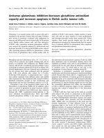
Figure 1a shows the schematic structure of the IOSCs.
In the fabrication of the IOSCs, firstly, a 50-nm ZnO
seed layer was deposited on fluorinated tin oxide (FTO)
substrate at a deposition temperature of 100°C by radio
frequency magnetron sputtering from a ZnO target. To
prepare flake-like AZO nanostructures, different
amounts of aluminum nitrate nonahydrate (Al(NO
3
)
3
·9H
2
O, 99.997%, Sigma-Aldrich, St. Louis, MO, USA)
were dissolved in a solution as an Al source t o fix its
concentration at 1, 2, and 4 mM, respectively. The solu-
tion for AZO nanostructure growth was an aqueous
solution of 0.025 M Zn(NO
3
)
2
·6H
2
OandHMT.The
reaction was kept at 100°C for 1 h, and the ZnO nano-
flakes (NFs) exhibited a length of approximately 100
nm, as shown in Figure 1b. Then, the fabricated samples
were removed from the solution, rinsed with distilled
water, and dried in air. The solution of poly(3-hexylthio-
phene)/(6,6)-phenyl C
61
butyric acid methyl ester
(P3HT/PCBM, 20:18 mg) in chlorobenzene (1.0 ml) was
deposited by spin coating at 1,000 rpm on the AZO NF
arrays. Afterwards, MoO
3
thin film of 10 nm thi ckness
and Al electrodes of 100 nm thickness were deposited
on P3HT/PCBM active layer via thermal evaporation at
the pressure of 10
-6
Torr. The thickness was measured
using the thickness monitor (Maxtek, Inc. USA). Finally,
the samples were annealed at 150°C for 8 min under
argon atmosphere (< 1 ppm O
2
and < 1 ppm H
2
O). The
active area of the IOSCs is 0.2 cm
2
. Figure 1c shows the
energy dispersive spectrum (EDS) of AZO
Figure 1 Schematic structure of the IOSCs, and FE-SEM images and EDS spectrum of AZO nanostructures.(a) The schematic structure of
the IOSCs based on AZO nanostructures. (b) The cross-sectional FE-SEM images of AZO nanostructure arrays fabricated on FTO substrates in an
Al concentration of 4 mM solution. Scale bar, 300 nm. (c) The EDS spectrum of AZO nanostructure array sample fabricated on the FTO substrate
in an Al concentration of 4 mM solution.
Fan et al. Nanoscale Research Letters 2011, 6:546
/>Page 2 of 6
nanostructures grown in a solution with 4 mM Al dop-
ing, which indicates the effective incorporation of Al
atoms into ZnO lattices.
Results and discussion
Figure 2a, b, c, d shows the field-emission scanning elec-
tron microscopy (FE-SEM) images for un-doped and Al-
doped ZnO nanostructures grown in a 0.025 M Zn
(NO
3
)
2
·6H
2
O and HMT solution with different Al con-
centrations from 1 to 4 mM. It is observed that the den-
sely packed ZnO NR arrays have grown almost on ZnO
seed layer without Al doping. Meaningfully, aft er the Al
concentrations are added in the solution, it is clearly
found that disperse and ultrathin flake-like AZO nanos-
tructures have grown. With increasing Al concentrations
from 1 to 4 mM, the density of the AZO NFs decreases
and the average size of the AZO NFs is 12.5, 13.6, and
15.0 nm, respectively, indicating that the smaller interfa-
cial area between flake-like nanostructures and the
active layer is achieved with increasing Al concentra-
tions from 1 to 4 mM. It is shown by EDS that the
atomic concentration of Al is 0.7%, 1.25%, and 1.47%
corresponding to 1, 2, and 4 mM Al doping,
respectively.
To increase the PCE of the IOSC devices, we firstly
optimize the MoO
3
thickness from 3 to 15 nm. Figure
3a shows the current-volt age (J-V) characteristics of the
IOSCs with different MoO
3
thicknesses from 3 to 15
nm, under simulated 100 mW cm
-2
(AM 1.5 G) solar
irradiation. It is illuminated that the PCE of the IOSC
devices reaches a maximum value of approximately
1.04% with 5 nm thickness of MoO
3
, which is attributed
to a relative complete coverage of the active layer by
MoO
3
, and thus avoiding certain leakage currents in
Figure 2 The SEM images of ZnO nanostructures grown in a solution with different Al concentrations.(a) 0 mM; (b) 1 mM; (c) 2 mM; (d)
4 mM. Scale bar, 300 nm.
Fan et al. Nanoscale Research Letters 2011, 6:546
/>Page 3 of 6
some weak spots [12]. As increasing the thickness fro m
10 to 15 nm, the J
SC
decreases from 8.87 to 8.18 mA
cm
-2
and the fill facto r (FF) decreases from 0.315 to
0.307, and as a result, the PCE decreases from 1.01% to
0.90%. Previous works had reported that MoO
3
has a
quite high electrical resistivity (>10
9
Ω cm) [ 13-15].
Therefore, the deterioration of the IOSC performance
may be induced by a higher intrinsic resistance of the
MoO
3
with 15 nm, restraining the ch arge transport
from the active layer to Al electrodes.
Figure 3b shows the J-V characteristics of the IOSC
devices with MoO
3
of 5 nm thickness and with flake-
like AZO nanostructures grown in a solution with Al
concentrations from 1 to 4 mM. The perf ormance para-
meters of the devices are also summarized in Table 1.
For the convenience of comparison, the length of the
AZO NFs is kept at approximately 100 nm. Clearly,
devices with un-doped ZnO have a bad performance:
J
SC
=8.56mAcm
-2
,open-circuitvoltage(V
OC
)=
0.360 V, FF = 0.337, and a PCE o f 1.04%. With doping
1and2mMAlconcentrations,theJ
SC
of devices
increases to 10.26 and 11.08 mA cm
-2
,andthePCE
increases to 1.26% and 1.44%, respectively. With
increasing Al concentrations to 4 mM, the J
SC
has
hardly any change at all; however, the FF increases
0.412, and as a result, the highest PCE of 1.65% is
achieved. The results indicate that the PCE of the
devices can be easily improved through a simple Al
doping into ZnO lattice process.
We reckon that the PCE improvement in the IOSCs is
almost attributed to the high s of the flake-like AZO
nanostructures. Previous works had reported the s of
un-doped and Al-doped ZnO whiskers synthesized via
hydrothermal method. The conductivities of un-doped
and Al-doped ZnO whiskers were calculated using the
following equation:
Figure 3 The J-V characteristics and the corresponding dark J-V characteristics.(a) The J-V characteristics of the IOSCs with different MoO
3
thickness from 3 to 15 nm under simulated 100 mW cm
-2
(AM 1.5 G) solar irradiation. (b) The J-V characteristics of IOSCs with Al concentrations
from 1 to 4 mM. (c) The corresponding dark J-V characteristics of IOSCs with different Al concentrations. (d) The J-V characteristics of devices
based on ZnO/P3HT hybrid solar cells.
Fan et al. Nanoscale Research Letters 2011, 6:546
/>Page 4 of 6
1
σ
= R
S
h
,
(1)
where s was the electrical conductivity, R was the
tested value of resisti vity, S was the area of the effective
measuring electrode, and h was the thickness of the
samples. It is found that the s of AZO whisker samples
significantly increased with the increase of Al concentra-
tions[16].Inthisstudy,thevalueofs is calculated
using the same method, as shown in Table 1. It is found
that the s increases dramatically from 8.2 × 10
-5
to 5.1
×10
-4
(Ω cm)
-1
with the increase of the Al concentra-
tions from 0 to 4 mM. Comp ared with the un-doped
ZnO nanostructures, the AZO nanostructures can pro-
vide a higher conduction pathway to enhance electron
transport from P3HT/PCBM matrix to FTO electrodes,
as can be clearly clarified in the dark current of devices
in Figure 3c. The AZO-based devices have a lower leak-
age current and R
S
than that of the un-doped ZnO-
based devices. The results are shown in Table 1. There-
fore, through increasing the s of the AZO to facilitate
electron transport, the J
SC
and PCE of IOSCs can be
strikingly improved.
In addition, we turn to consider that a suitable mor-
phology of AZO NF array, such as the density of AZO
NF arrays, could account for the performance increase
intheIOSCs.Asiswellknown,thelowestunoccupied
molecular orbital (LUMO) level of ZnO is -4.2 eV and
the LUMO level of P3HT is -3.0 eV [17]. It suggests
that electrons can be injected from the LUMO of P3HT
into the LUMO of ZnO. In this study, upon the Al-dop-
ing treatment, it is interesting to observe that the ultra-
thin and disperse AZO NF arrays have grown on the
densely packed ZnO NR array. Generally, the ultrathin
and disperse AZO NFs could reach the matrix of
P3HT/PCBM, providing a continued “ tentacles” for elec-
tron collection from PCBM clusters to FTO electrodes.
At the same time, owing to the achievement of higher
density of AZO NFs, the larger area of interface between
AZO NFs and P3HT crystals may induce more suffi-
cient exciton dissociation. The above two factors could
explain why the J
SC
of IOSCs would drop slightly as
increasing Al concentration from 2 to 4 mM, even if the
s continues to increase.
To better understand the role of the AZO morphology
on the performance of the IOSCs and eliminate the
possible effect of different PCBM cluster aggregations
on the IOSC performance simultaneously, we fabricated
two hybrid solar cells A and B with the structure of
FTO/ZnO seed layer/AZO nanostructures/P3HT/Al.
The AZO nanostructures, synthesized in a solutio n of 2
and 4 mM A l concentrations respectively, have a signifi-
cant variety in morphology, such as the density and the
size. The J-V characteristics of the IOSC devices are
presented in Figure 3d. It has been found that the s
increases with the increase o f Al concentrations from 2
to 4 mM; however, the J
SC
decreases from 2.73 to 2.37
mA cm
-2
and the FF increases from 0.311 to 0.320, and
as a result, the P CE decreases from 0.22% to 0.19%. It
suggests that less interfacial area betw een the P3HT and
the AZO nanostructures induces a less exciton dissocia-
tion, even though AZO nanostructures of a higher s
have been achieved through more Al doping into ZnO
lattices. Therefore, a sufficient interface contact for exci-
ton dissociation between P3HT and AZO nanostruc-
tures should account for the increase in the PCE of
IOSCs.
Conclusions
In conclusion, we fabricated the IOSCs based on the
flake-like AZO nanostructures with controllable s and
morphology via a simple hydrothermal method. The
effects of the electrical property and morphology charac-
teristics of flake-like AZO nanostructures on the perfor-
mance of the IOSC devices were investigated. It i s
found that the PCE of the IOSC devices depends criti-
cally on the s of AZO nanostructures and the i nterface
area between the flake-like AZO nanostructures and the
active layer. These results suggest that the flake-like
AZO nanostructures could be a promising potential
candidate in various photovoltaic and optoelectronic
applications to improve device performance.
Acknowledgements
This work was supported by the National High Technology Research and
Development Program of China (2009AA03Z219), 973 Program (no.
2011CB933300) of China, the National Natural Science Foundation of under
grant no. 11074194, the Research Program of Suzhou Science & Technology
Bureau (SYG201133) and the Fundamental Research Funds for the Central
Universities (201120202020001).
Authors’ contributions
All authors contributed equally and read and approved the final manuscript.
Table 1 Device performance parameters of the IOSCs and the corresponding electrical conductivity
Sample J
SC
(mA cm
-2
) V
OC
(V) FF PCE (%) R
S
(Ω cm
2
) s (Ω cm)
-1
Size (nm)
0 mM 8.56 0.360 0.337 1.04 31.5 8.2 × 10
-5
-
1 mM 10.26 0.375 0.328 1.26 22.7 3.2 × 10
-4
12.5
2 mM 11.08 0.370 0.351 1.44 17.8 4.4 × 10
-4
13.6
4 mM 10.97 0.365 0.412 1.65 14.4 5.1 × 10
-4
15.0
IOSCs are based on ZnO nanostructures grown in a solution with different Al concentrations from 0 to 4 mM.
Fan et al. Nanoscale Research Letters 2011, 6:546
/>Page 5 of 6
Competing interests
The authors declare that they have no competing interests.
Received: 8 May 2011 Accepted: 4 October 2011
Published: 4 October 2011
References
1. Greene LE, Law M, Yuhas BD, Yang PD: ZnO-TiO(2) core-shell nanorod/
P3HT solar cells. J Phys Chem C 2007, 111:18451.
2. Liu JP, Wang SS, Bian ZQ, Shan MN, Huang CH: Organic/inorganic hybrid
solar cells with vertically oriented ZnO nanowires. Appl Phys Lett 2009,
94:173107.
3. Liu NS, Fang GJ, Zeng W, Long H, Fan X, Yuan LY, Zou X, Liu YP, Zhao XZ:
Strong Effect of Interelectrode Distance on the Performance of a Novel
ZnO Nanorod Lateral Field Emission Device Fabricated by a Single-Step
Hydrothermal Approach. J Phys Chem C 2010, 114:8575.
4. Shin KS, Lee KH, Lee HH, Choi D, Kim SW: Enhanced power conversion
efficiency of inverted organic solar cells with a Ga-doped ZnO
nanostructured thin film prepared using aqueous solution. J Phys Chem
C 2010, 114:15782.
5. Lin Y-Y, Lee Y-Y, Chang LW, Wu J-J, Chen C-W: The influence of interface
modifier on the performance of nanostructured ZnO/polymer hybrid
solar cells. Appl Phys Lett 2009, 94:063308.
6. Wu SJ, Tai QD, Yan F: Hybrid Photovoltaic Devices Based on Poly (3-
hexylthiophene) and Ordered Electrospun ZnO Nanofibers. J Phys Chem
C 2010, 114:6197.
7. Li YJ, Lu MY, Wang CW, Li KM, Chen LJ: ZnGa
2
O
4
nanotubes with sharp
cathodoluminescence peak. Appl Phys Lett 2006, 88:143102.
8. Wang H, Baek S, Song J, Lee J, Lim S: Microstructural and optical
characteristics of solution-grown Ga-doped ZnO nanorod arrays.
Nanotechnology 2008, 19:075607.
9. Bae SY, Na CW, Kang JH, Park J: Comparative structure and optical
properties of Ga-, In-, and Sn-doped ZnO nanowires synthesized via
thermal evaporation. J Phys Chem B 2005, 109:2526.
10. Xue XY, Li LM, Yu HC, Chen YJ, Wang YG, Wang TH: Extremely stable field
emission from AlZnO nanowire arrays. Appl Phys Lett 2006, 89:04311.
11. Yun SN, Lee J, Yang J, Lim S: Hydrothermal synthesis of Al-doped ZnO
nanorod arrays on Si substrate. Physica B 2010, 405:413.
12. Zhao DW, Tan ST, Kec L, Liu P, Kyaw AKK, Sun XW, Lo GQ, Kwong DL:
Optimization of an inverted organic solar cell. Solar Energy Materials &
Solar Cells 2010, 94:985.
13. Miyata N, Akiyoshi S: Preparation and electrochromic properties of RF-
sputtered molybdenum oxide films. J Appl Phys 1985, 58:1651.
14. Julien C, Khelfa A, Hussain OM, Nazri GA: Synthesis and characterization of
flash-evaporated MoO
3
thin films. Journal of Crystal Growth 1995, 156:235.
15. Navas I, Vinodkumar R, Lethy KJ, Detty AP, Ganesan V, Sathe V, Mahadevan
Pillai VP: Growth and characterization of molybdenum oxide nanorods
by RF magnetron sputtering and subsequent annealing. J Phys D: Appl
Phys 2009, 42:175305.
16. Huang SP, Xiao Q, Zhou H, Wang D, Jiang WJ: Hydrothermal synthesis
and conductive properties of Al-doped ZnO rod-like whiskers. Journal of
Alloys and Compounds 2009, 486:L24.
17. Hames Y, Alpaslan Z, Kösemen A, San SE, Yerli Y: Electrochemically grown
ZnO nanorods for hybrid solar cell applications. Solar Energy 2010, 84:426.
doi:10.1186/1556-276X-6-546
Cite this article as: Fan et al.: Controllable synthesis of flake-like Al-
doped ZnO nanostructures and its application in inverted organic solar
cells. Nanoscale Research Letters 2011 6:546.
Submit your manuscript to a
journal and benefi t from:
7 Convenient online submission
7 Rigorous peer review
7 Immediate publication on acceptance
7 Open access: articles freely available online
7 High visibility within the fi eld
7 Retaining the copyright to your article
Submit your next manuscript at 7 springeropen.com
Fan et al. Nanoscale Research Letters 2011, 6:546
/>Page 6 of 6