Optical Fiber Communications and Devicesan incorrectly Part 15 pot
Bạn đang xem bản rút gọn của tài liệu. Xem và tải ngay bản đầy đủ của tài liệu tại đây (1.93 MB, 25 trang )
Design of Advanced Digital Systems Based on High-Speed Optical Links
339
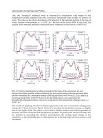
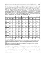
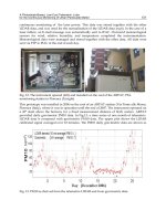
Fig. 1. Image of a comercial SFF optical transceiver.
In order to achieve faster switching and to increase immunity to EMI, crosstalk and noise,
high-speed data links work over differential signals. In the case of high speed optical data
links, both the electrical input and output signals are typically LVPECL signals (Low-
voltage positive emitter-coupled logic). LVPECL is a power optimized version of PECL
(uses 3.3 V instead of 5V supply), and both are differential signalling systems mainly used in
high speed and clock distribution systems. This technology achieve high speed data rates by
using an overdriven BJT differential amplifier with single-ended input, whose emitter
current is limited to avoid the slow saturation region of the transistor operation. In Figure 2,
a block diagram of a generic optical transceiver is shown.
Fig. 2. Transceiver functional diagram.
Optical Fiber Communications and Devices
340
2.3 Electronic components for signal conditioning
As mentioned before, optical links can reach quite high data rates, up to 10 Gbps, that
can not be easily handled by the electronic circuitry. Usually, the serial data received
by the optical data link is split into several electronic data channels, each of them
working at a lower data rate, so they can be properly processed by the electronic
components and devices. When transmitting, several electronic data channels are combined
onto a single data channel at a high data rate and then is optically transmitted. This
aggregation/disaggregation process is performed by electronic serializer/deserializer
devices. A serializer receives data information from N inputs at a given data rate and
combine them into a single data channel at a data rate N times faster. When working as
deserializer the process is the opposite. The deserializer receives a single data chunk and
breaks it into N data channels at a data rate N times slower. So the PCB and the electronic
circuitry do not have to operate at the high data rates provided by the optical link.
To serialize data at high speeds, the serial clock rate must be an exact multiple of the clock
for the parallel data, so most of electronic designs for high speed optical links use a PLL to
multiply a reference clock running at the desired parallel rate to the required serial rate.
Moreover, when serial data are received, the optical transceiver must use the same serial
clock that serialized the data to deserialize it. At high line rates, providing the serial clock
with a separate wire is very impractical because even the slightest difference in length
between the data line and the clock line can cause significant clock skew. Instead, optical
transceivers recover the clock signal from the data directly, using transitions in the data to
adjust the rate of their local serial clock so it is locked to the rate used by the other optical
transceiver. Systems using Clock Data Recovery (CDR) can operate over much longer
distances at higher speeds than their non-CDR counterparts. However, if transmitted data
has too few transitions, the receiving optical transceiver can be unable to apply CDR
techniques, so the electronic implementation of encoding schemes is required, as 8B/10B, in
which each octet of data is mapped to a 10 bit sequence, or 64B/66B, in which data are
grouped into sets of 64 bits, scrambled, then prepended with a 2 bit header.
Additionally, most systems require some form of error detection and correction, as
encoding-based error detection or Cyclic Redundancy Checks (CRCs). All this electronic
signal conditioning hardware requires quite complex design tasks in order to properly
connect the data received/transmitted by the high speed optical link and the processing
unit. A simplified block diagram of an optical data link is shown in the figure below.
Fig. 3. Optical data link electronic blocks.
2.4 High speed digital data processing
The information carried by the data signals has to be generated and processed. To handle
the huge amount of information transmitted by the high speed optical links parallel
Design of Advanced Digital Systems Based on High-Speed Optical Links
341
processing is required, so FPGAs are used. A FPGA is an integrated circuit designed to be
configured by the designer after manufacturing. FPGAs contain programmable logic
components called "logic blocks", and a hierarchy of reconfigurable interconnects that allow
the blocks to be "wired together", so many logic gates that can be inter-wired in many
different configurations. Logic blocks can be configured to perform a huge amount of
complex combinational functions. In most FPGAs, the logic blocks also include memory
elements, which may be simple flip-flops or more complete blocks of memory.
A FPGA can also include multipliers, so it can be used for digital signal processing
functions. Once the FPGA internal circuits have been hardware interconnected to perform a
given functionality, the FPGA can perform parallel data processing at a very high speed, in
the order of hundreds of MHz. So that is the reason for its wide use together with high
speed data links.
Moreover, very impressive advances have been done in recent years related to FPGAs
configuration capabilities. Nowadays it is possible to implement inside the FPGA a great
variety of electronic building blocks and peripherals, for instance, 32-bits hardware
microprocessors as MicroBlaze® from Xillinx. These advances include the implementation
of MultiGigabit Transceivers (MGT) inside the FPGA. These transceivers performs all the
electronic signal conditioning described in section 2.3, so the optical transceiver can be
connected almost directly to the FPGA input/output ports. These MGTs manage all the
aspects of communication with optical transceivers, as signal integrity,
serialization/deserialization, terminations and coupling, line rates, encoding, clock
correction, latencies, etc. So the FPGA embedded MGTs are a great improvement for high
speed optical links because they simplify the electronic hardware design and reduce the
project development costs. Figure 4 shows a building block of the typical MGT
functionality.
Fig. 4. MGT building block configuration.
Optical Fiber Communications and Devices
342
3. Optical links design considerations
Optical fiber links are typically used for high-speed data transmissions. In such scenarios,
several specific issues need to be taken into account. In this section, the most common
problems in high-speed PCB design will be enumerated and briefly described. Some
suggestions will be also given in order to minimize them. The key points to be considered
are the transmission lines, crosstalk, differential traces, decoupling and power system, EMI,
clock signals and other specific considerations.
3.1 Transmission lines
Lossy transmission lines are common on printed circuit boards. Signals travelling at high
frequencies through narrow strips are affected by the skin effect and the dielectric losses,
producing signal distortion. In a basic model, transmission lines can be described as formed
by a network of inductors, capacitors and resistances, as it is shown in Figure 5. At high
frequency, these effects appear, causing reflections and attenuations of the signal.
Fig. 5. Distributed parameters transmission line model.
In this sense, the characteristic impedance of a transmission line needs to be introduced as
its fundamental parameter. It is defined by the following expression:
0
L
Z
C
In order to reduce the reflections, the characteristic impedance (Z
0
) of the line should be
matched to the source impedance (Z
s
) as well as to the load impedance (Z
L
). This matching
procedure can be carried out by using several types of matching networks:
Single Parallel Termination.
Thevenin Parallel Termination.
Active Parallel Termination.
Series-RC Parallel Termination.
Series Termination.
Differential Pair Termination.
On-Chip Termination.
Diode Termination.
A common problem in high-speed PCB design is the formation of undesired stubs. These
stubs are non-terminated transmission line segments that generate impedance mismatching,
and then, undesired reflexions. Stubs can appear from single non-terminated lines, pins,
unfinished IC’s or non-terminated segments acting as antennas, as illustrated in Figure 6. In
Design of Advanced Digital Systems Based on High-Speed Optical Links
343
order to avoid unexpected stubs, the length or the strips must be reduced at maximum and
all the unused pins should be connected to ground or power.
short
Stub
too
long
Stub
short
Stub
Zo
Antenn
a
Stub
Fig. 6. Stubs examples.
3.2 Crosstalk and differential traces
Coupling between signals appears due to induced voltage from one line to another one. The
magnetic coupling is produced by the mutual inductance, while the electric coupling is
represented by mutual capacitances. This is represented in Figure 7. The undesirable energy
coupled between lines is called crosstalk. Switching signals travelling in the same direction
and driving the same current are in even mode. Otherwise they are in odd mode.
Fig. 7. Crosstalk between traces.
For reducing this effect a number of considerations are listed:
Use, when possible, strip-lines. They are strips placed between planes, acting as
shielding.
Use, when possible, proper stack-up, by placing the traces as close as possible from
their reference planes. This will help to uncoupling nearby signals and will couple it to
the reference plane.
Separate tracks as far as possible. Use the rule: the distance between the middle of
traces must be four times the trace width.
Optical Fiber Communications and Devices
344
Use terminations to reduce the crosstalk.
Minimize the signal return loops. If it exists a significant coupling between signals of
contiguous layers, both should be orthogonal to each.
Another very important consideration in order to reduce crosstalk is using differential
routing techniques (see Figure 8) since, in this way, ground noise related problems are
avoided by providing high noise margins. In addition, the inductance influences are
cancelled. Due the differential signals have the same length and they are opposite, there is
not signal return through ground. Switching times can be more accurate if these kinds of
signals are used instead of single-ended signal.
Fig. 8. Differential signal.
The key point when dealing with this kind of signals is setting the lines with the same
distance in order to keep the signals in phase. Otherwise, the power integrity should be
affected. It is possible to give a number of recommendations regarding the design of this
kind of lines:
The traces must have the same length. This is because the delay must be minimum.
Otherwise, it could generate serious EMI problems due to the appearance of common
mode currents. Another problem is caused by the induced current on the plane, acting
as crosstalk.
Keep the loop area minimum. The traces must be routed as close as possible, even
eliminating the planes that are below of differential traces and removing induced loops.
When dealing with differential traces very close to each other, terminations for reducing
coupling should be used. For selecting the appropriate termination, impedance
calculations can be required.
The separation between lines must be constant along them. Try to avoid layer changes,
so routing in the same layer, and try to avoid using traces between two lines forming a
differential pair.
Try to avoid the use of vias. They introduce losses and an impedance steps. If we need
to use them, in transitions, place them next to each other for maintaining the differential
impedance ratio.
3.3 Decoupling and power systems
It is indispensable to know which is the current return of a high-speed signal. An effect,
called ground bounce, will produce to cause a reference level increase. The effect is caused
by the short switching times. They cause high transients current and discharge load
capacitances. Load capacitance, inductance of the connectors and the number of switching
are the predominant factors to increase the effect. For this reason, capacitors should be
placed near devices and parasitic inductances that contribute to the ground bounce. This
effect is shown in Figure 9.
Design of Advanced Digital Systems Based on High-Speed Optical Links
345
Fig. 9. Ground bounce effect over signal.
The uncoupling of power supplies provides benefits on power integrity, signal integrity and
highly reduces EMI.
Small capacitors usually display better performance at high frequency regimes, but they also
usually display higher inductances than bigger ones. Each capacitor has a recommended
frequency band usage, described by its equivalent series resistance (ESR) and the quality
factor (Q). To reduce its inductance, the capacitor should be placed as close as possible to the
power source. It is recommended to connect it directly to the power and reference plane,
avoiding any surrounding traces around it. The distance should not be more than quarter of
wavelength.
In the frequency response of a capacitor there is a point called resonance point where the
value of the impedance of the equivalent LC circuit is zero, as shown in Figure 10. From this
point, the capacitor behaves like an inductor rather than a capacitor. The use of multiple
capacitors in parallel does not change the resonance frequency but increases the capacitance
effect, so reducing the individual inductance and the ESR.
The impedance response in power systems can be improved by the increasing of the number
of capacitors and by considering capacitors with moderate ESR.
Fig. 10. Frequency response of the inductance of capacitors in parallel.
Optical Fiber Communications and Devices
346
Other considerations that we should follow are:
Eliminate connectors when possible.
Use multilayer PCBs.
Connect the capacitor pad in the plane through big vias to minimize the inductance and
so helping the current flow.
The traces travelling from power pins to planes must be wide and short in order to
reduce the serial inductance, so decreasing the ground bounce.
Connect each ground pin or via in the plane individually.
The signal returns that go through connectors must have ground connections with the
same potential. For this, the use of several returns (ground) for each one or two signals
is necessary.
Using antipads reduces coupling between the connector and the ground or power
plane.
For isolating the high frequency noise, local filtering is recommended. Ferrites, requiring a
big size capacitor to keep the output impedance in a reasonable level, are usually used.
Another point is which considerations take into account when using analog and digital
sections in power systems. Variations in voltage gradients can be produced, due to the high
frequency of returning currents or to the current that flows through the planes from
regulated sources. These variations produce the charge and discharge of the bypass and
planar capacitors of the circuit, therefore generating noise. To avoid the noise generated for
another circuit sections different power supplies distributed in different regions of the
circuit can be used. It can be used different voltage power distributed in the same plane. If
each power section requires its own distribution plane, then they should have their own
reference plane. All reasons to use planes go in the same direction: noise control.
Some of the rules regarding the use of planes are the following:
Planes must be routed separately, in star. When multiples islands of power supply are
routed in the board, they must be connected to a single point through 0-ohm resistors or
ferrites. Often, the analog ground is joined to the digital ground, in this way.
Do not allow sections of analog power to be placed above or below a region of digital
plane. The components must be efficiently placed and grouped with their planes
without overlap with other circuits (Figure 11).
Be careful when uncoupling. Do not bypass erroneous references that may cause noise
coupling between planes.
Do not track traces if its current return has a discontinuity or gap. They will have a big
loop and EMI problems can appear.
If the power plane shares analog and digital supply, both sections must be separated.
Then, the components should be placed in their respective planes.
Each high-speed line must be referenced with its contiguous plane, for reducing loop,
controlling the impedance and the crosstalk.
The layer stack is very important for reducing loops and having the control of the
capacitance between planes as well as having EMI control. A good design is characterized
by having each trace referenced to nearby planes and each power supply, providing a
capacitance between planes. A good layer stack example is shown in Figure 12.
Design of Advanced Digital Systems Based on High-Speed Optical Links
347
Fig. 11. Trace overlapping a not related plane.
GND
Signal
Power
GND
Signal
GND
Signal
GND
Signal
Power
GND
Signal
GND
Signal
Signal
Power
GND
Signal
Signal
GND
Signal
Power
GND
Signal
Signal
GND
GND
Signal
6-Layer
8-Layer
Fig. 12. Good stack layer for 6 and 8 layers.
As it can be seen, it is always preferred a layer stack where the signal layers are placed
between two planes. If using many signal layers is necessary, two signal layers can be
contiguously placed, although they should be orthogonally routed, in order to avoid
couplings.
3.4 Electromagnetic Interferences (EMI)
Electromagnetic interferences are directly proportional to the change in current or voltage as
a function of the time and the serial inductance of the circuit. PCBs always generate EMI, so
a number of considerations for minimizing them should be taken into account.
Place each signal layer between ground plane and power plane. Inductance is directly
proportional to the distance. The shorter distance, the lower inductance.
Select low inductance components, like surface mount devices (SMD).
Reduce return paths by using solid ground planes. Keep the signal and the return as
close as possible each to other. Remember that current return travels through the
minimum impedance path.
Place capacitors near connectors or devices.
The use of strip lines adds an extra control on EMI.
Avoid the use of stubs. They can behave like antennas.
Optical Fiber Communications and Devices
348
One of the main sources of EMI is the current loop. The other is common mode problems.
The differential mode is the mode where the signals travel forming a path and a return in
opposite direction. When signals travel in the same direction, both signal and return, is
called common mode. This occurs because the ground is not a perfect driver and there is an
undesired associated inductance. This effect is illustrated in Figure 13.
Fig. 13. Common and differential mode.
The main considerations in order to reduce this effect are the following:
Keep a solid reference and continuous plane for each line. Trace the critical lines as
striplines.
Reduce presence of stubs.
Ensure that exists a good capacitive coupling between planes.
3.5 Clock transmission line
We have mentioned differential lines but we have not introduced single-ended lines
connecting a source with load or receiver. They are used in point-to-point routing, signal
clock routing, low-speed lines and non-critical I/O lines. Signal clock routing is the most
remarkable point in single-ended lines. The following considerations are given to improve
signal integrity in clock signals:
Keep lines as straight as possible. Use rounded shapes instead of sharp angled ones.
Do not use multiple signal layers for clock signals.
Do not use vias in clock lines. They change the impedance and they cause reflexions.
Place a ground plane next to the outer layer to minimize the noise. If you use inner
layers for routing a clock trace, form a sandwich with both layers.
Use terminations to minimize reflexions.
Use point-to-point traces.
The clock signals can be routed in several ways. If a daisy chain routing is used, undesired
stubs or short traces can appear, so degrading the signal quality and producing reflexions.
When considering a star routing, the clock signal arrives to all devices at the same time, so
lines must have the same length. Each load must be identical for minimizing signal integrity
problems. To design traces with the same length, serpentine techniques for time adjusting
are used. Several types of clock signal routing are illustrated in Figure 14.
Design of Advanced Digital Systems Based on High-Speed Optical Links
349
D1 D2
Rt
Stub
Clock
D1
D2
D3
Rt
Rt
Rt
Clock
D1
D2
Rt
Rt
Clock
Fig. 14. Types of clock signal routing.
3.6 Other considerations
In high-speed designs other considerations are taken into account, depending on the
amount of information needed to be sent.
For example, at data rates of 622 Mbps and higher, the skin effect is extremely important.
This could cause signal attenuations over long distances. The result is a low pass filter with
attenuation, which increases with frequency. For this reason, the traces should be wider.
On the other hand, connectors and vias cause impedance discontinuities. In order to reduce
them, specific connectors with shielding features with many ground connections must be
used.
High-performance cables are also very important to have a good bandwidth and for
minimizing attenuation losses.
When working at 2.5 Gbps and beyond, the problems become substantially more difficult to
eliminate. There are many copper and dielectric losses. It is needed to pay attention to every
consideration for PCB and layout design. A backplane thickness of less than 0.200 inches
gives the best result. Vias used for interconnection between layers create line discontinuities.
These routed layers should be as few as possible and thus limiting the number of vias, so the
vias are shorter, minimizing line discontinuities. Buried vias can be used to reduce this
problem in thicker boards.
The material used in boards is very important. FR4 dielectric commonly used has significant
losses above 2 Gbps. For this reason, low-loss dielectric PCB material can be used such as
Rogers 4350, GETEK or ARLON.
4. Signal integrity studies
Digital system design has therefore moved deep into the Multi-GHz range, with signal rise
and fall-times of the order of 100ps or less. It is a well-known fact that Signal Integrity (SI)
simulations become necessary when system designs break the 50-100MHz barrier, and are
virtually mandatory in the GHz range. SI simulations are used to ensure the quality and
accurate timing of electrical signals. The benefits of SI analysis early in the design cycle are
well established, as it allows the identification and resolution of SI problems like overshoot,
ringing, crosstalk, delay mismatches, etc. before the first prototype is built.
Optical Fiber Communications and Devices
350
4.1 Pre-layout studies
The pre-layout simulations are required at the earliest stages of the PCB design. In this stage
the designer evaluates several topologies and selects the one that fulfils all the specifications
such as size, component number and performance. In addition, the results of these
simulations help to set crucial parameters for the transmission structure, such as trace
width, trace spacing, maximum trace length, and critical component placement. It is
important to understand these simulations are intended for selecting the components and
topologies as well as for fine tuning of the signal path. The results analysis is used to set the
rules that will be incorporated into the layout.
As an example, and taking into account the design considerations described in the previous
section, a real design is going to be studied. The main elements in this design are:
SFP Optical Connector with two receiver channels (1)
Transmitter/Receiver Chip Set (2)
FPGA (3)
Fig. 15. Elements of Advanced Digital Systems based on High-Speed Optical Links in PCB.
The optical connector has a differential output (LVPECL), routed to the entrance of
Transmitter/Receiver Chip Set. These transmission lines are the most critical of the study
because is a point-to-point serial data transmission with a very high bit rate.
Another point to be taken into account is the connection between data acquired in the
Transmitter/Receiver Chip Set and the FPGA. In this case, the importance of the study is not
based in data frequency. We must avoid the data bus crosstalk.
4.1.1 Differential lines
This signal has a critical jitter and the topology, geometry, length, and termination
impedance must be carefully studied. In this case, it is observed the differential line without
being routed.
Design of Advanced Digital Systems Based on High-Speed Optical Links
351
Fig. 16. Unrouted differential lines.
The topology is extracted according to the manufacturer's datasheet optical connector.
Fig. 17. Extracted topology.
An ideal study without transmission line is performed. The simulation for this case is:
Fig. 18. Waveforms for differential lines.
Optical Fiber Communications and Devices
352
In black and green color RX+ and RX- signals are observed and in blue color the resulting
differential signal is presented. The voltage values obtained are the same that the
manufacturer recommendations.
The next step, seeing the topology is correct, it would add a transmission line and observe
the maximum length that could have the routing. In the next section another types of line
will be studied.
4.1.2 Parallel data bus
In this case, the connection between the transmitter/receiver chip set and the FPGA is
studied. Its speed of transmission is not comparable with that of the differential line. Even
so, the maximum length must be checked and a termination may be needed.
First, a study of a single line to detect maximun length and optimal termination has to be
performed. The study was performed for a bus of 32 lines at 80 MHz.
Fig. 19. Topology of single-ended line.
The waveforms for each length (800, 5000, 9000 y 12000 mils) are as follows:
Fig. 20. Waveform for single-ended line.
Design of Advanced Digital Systems Based on High-Speed Optical Links
353
The waveforms 800, 5000, 9000 y 12000 mils in black, green, red and blue provide a delay to
the length, which increases to approximately 2.14 ns in the worst case. This shows a
mismatched line. Also the waveforms will degrade depending on the length of the track due
to the increasing influence of the reflections, since an overshoot and ringing growing.
The worst case above (12000 mils) but with a termination is now studied. The topology is:
Fig. 21. Topology of single-ended line with active termination.
The results are:
Fig. 22. Waveform of single-ended line with active termination.
Optical Fiber Communications and Devices
354
Which greatly improves the previous case:
Fig. 23. Waveform of single-ended line without termination.
Working with a data bus is essential to examine the crosstalk between the lines. The
topology studied is as follows:
Fig. 24. Topology of three parallel lines.
Design of Advanced Digital Systems Based on High-Speed Optical Links
355
Where there are three bus lines, taking the top and bottom as aggressors and the middle line
as victim.
The results for high steady state are:
Fig. 25. Waveforms of three parallel lines.
In blue and green color, we have waveforms of the FPGA inputs, that correspond to the
agressor signal. The red one is the receiver input that flowing by the victim trace, and the
black one is the output driver of the victim trace. In this case a crosstalk about 2149mV is
obtained and the simulation does not pass the test (the victim signal is in an undefined logic
state, below 3V).
In the previous section is commented that the solution is adapting the transmission lines
using terminations. If an active termination is added to the lines and then the simulation is
made in each line, the result is as follows.
Fig. 26. Topology of three parallel lines with active termination.
Optical Fiber Communications and Devices
356
Fig. 27. Waveforms of three parallel lines with active termination (high level).
It can be observed a clear improvement in the crosstalk level, keeping the victim signal
inside the permitted high level range. However, at low level it is shown a crosstalk of 1421
that causes the victim signal introduces in the forbidden region for low level, and this can
cause errors.
Fig. 28. Waveforms of three parallel lines with active termination (low level).
Then, the initial solution of placing an active termination is not suitable. As theory says, we
should test a serial termination and check what happen.
Design of Advanced Digital Systems Based on High-Speed Optical Links
357
Fig. 29. Topology of three parallel lines with serial termination.
In this case, crosstalk level keeps the victim signal within the permissible limits either in/for
high level (figure 30) or low level (figure 31). The values are 1365 mV for high level and 1514
mV for low level.
Fig. 30. Waveforms of three parallel lines with serial termination (high level).
Fig. 31. Waveforms of three parallel lines with serial termination (low level).
Optical Fiber Communications and Devices
358
4.2 Post-layout studies
When the layout is complete, a post-layout simulation is performed on the critical sections
of the board to ensure there are no major signal integrity problems. Based on the results of
the post-layout simulation, any changes required are incorporated in the layout and the
layout is released to the fabrication house for board manufacturing. The post-layout
simulation process requires the layout of all active layers on the board as well as the
physical properties of the dielectric and metal layers. The post-layout simulations use the
physical properties supplied by the fabrication house that may differ from those published.
4.2.1 Differential lines
Taking the pre-layout studies conducted on the differential lines and after to route them
with the defined conditions, we extract the real topology that will be sent to the
manufacturer for verification.
Fig. 32. Real topology of differential lines.
We can see that actual results match those obtained in the ideal simulation (Figure 18):
Fig. 33. Real waveforms of differential lines.
Design of Advanced Digital Systems Based on High-Speed Optical Links
359
4.2.2 Parallel data bus
In this case, as in the above, we extract the real topology. We studied a serial termination in
bus line.
Fig. 34. Real topology of parallel data bus.
The results are as expected, we see that the data sent between the transmitter/receiver chip
set and the FPGA function properly at the selected frequency and the distance routed.
Fig. 35. Real waveforms of parallel data bus.
5. Conclusions
The wide range of applications of optical fibers has been continuously supported by their
friendly integration with classic electronics. Being the optical transceiver the key element in
such hybrid systems, their design is not straightforward, and need to take into account a
good number of particularities.
In this chapter the main handicaps when developing electronics specifically for high-speed
fiber optic communications have been highlighted. Some of these issues fully lay in the field
Optical Fiber Communications and Devices
360
of electronic engineering. Other aspects, and due to the high frequency involved in such
systems, need some additional analysis. In this sense, the electromagnetic theory, as used for
wave propagation in dielectric materials, has to be applied to the electric transmission lines
present in some cases.
Being experiments the common analysis tools in hybrid opto-electronic systems, some
simulation tools can be sometimes used for fixing specific problems like cross-talking. These
numerical tools are of particular interest for proper routing design in PCBs.
After all, these systems have demonstrated their applicability in a huge number of scenarios
including communications, medicine, nuclear research, etc.
6. References
[1] Douglas Brooks, “Signal Integrity Issues and Printed Circuit Board Design”, Prentice
Hall PTR, 2003. ISBN: 0-131-41884-X
[2] Stephen C. Thierauf, “High-Speed Circuit Board Signal Integrity”, Artech House Inc.,
2004, ISBN: 1-58053-131-8
[3] Mark. I. Montrose, “Printed Circuit Board Design Techniques for EMC”, Wiley-
Interscience-IEEE, 2000, ISBN: 0-7803-5376-5
[4] Lattice Semi, “High-Speed PCB Design Considerations”, Technical Note TB1033, 2011.
[5] Altera, “High-Speed Board Layout Guidelines”, Application Note 224, 2009.
[6] Sackinger, E., “Broadband circuits for optical fiber communication”, Wiley, 2005. ISBN:
9780471712336
[7] Cox, C.H., “Analog optical links: Theory and practice”, Cambridge University Press,
2004. ISBN: 0-521-62163-1
[8] Muller, P., Leblebici, Y., “CMOS Multichannel Single-Chip Receivers for Multi-Gigabit
Optical Data Communications (Analog circuits and signal processing)”, Springer,
2010. ISBN: 978-90-481-7473-7
[9] ATLAS Trigger and DAQ steering group, “Trigger and Daq Interfaces with FE systems:
Requirement document. Version 2.0”, DAQ-NO-103, 1998.
[10] Dowell, M. Pearce, “ATLAS front-end read-out link requirements”, ATLAS internal
note, ATLAS-ELEC-1, July 1998
[11] J. Torres, “Estudio, diseño e implementación del módulo de preprocesado de datos del
Sistema Read Out Driver para el calorímetro TileCal del experimento ATLAS/LHC
del CERN”, Tesis Doctoral, Servicio de Publicaciones de la Universidad de
Valencia, Junio 2005.
[12] J. Torres et al, “Signal integrity studies at optical multiplexer board for tilecal system”,
2007 IOP Publishing Ltd and SISSA.
[13] Lynne Green, “Signal Integrity”, IEEE Circuits and Devices, November 1999.
[14] Jim Lipman, “Models make the difference in high-speed pc-board design”, Electronic
Design News, 15th April 1999.
17
Fiber Optic Temperature Sensors
S. W. Harun
1,2
, M. Yasin
1,3
, H. A. Rahman
1,2,4
, H. Arof
2
and H. Ahmad
1
1
Photonic Research Center, University of Malaya, Kuala Lumpur
2
Department of Electrical Engineering,
University of Malaya, Kuala Lumpur
3
Department of Physics, Faculty of Science and
Technology, Airlangga University, Surabaya
4
Faculty of Electrical Engineering, Universiti
Teknologi MARA (UiTM), Shah Alam
1,2,4
Malaysia
3
Indonesia
1. Introduction
The need for temperature measurement exists in many applications such as in automated
consumer products, automated production plants and high performance processors. Recent
works have mainly focused on temperature sensors that satisfy user requirements for
specific applications, and the main considerations are performance, dimension and
reliability. In fact, traditional low-cost solutions, such as thermocouples and resistance
temperature detectors (RTDs), do not always yield satisfactory performance, e.g., when the
fluid temperature has to be measured in hostile environments, in the presence of
electromagnetic, chemical, and mechanical disturbances. Since signals from the
thermoelectric sensors are normally mixed with intrinsic noise and extrinsic interferences,
they may contain intolerable errors if not properly filtered. Therefore, this type of sensors is
inept for gauging temperature in microfluidic or nano-sized devices, in extreme marine
environments, and underground geological sites where long distance measurement with
precision is required. For such applications, fiber optical sensors offer a better alternative
since the optical signal does not suffer from interference by electromagnetic fields and can
be transmitted over extremely long distances without any significant loss [Yasin et al., 2010;
Li et al., 2010; Ahmad et al., 2009; Lim et al., 2009; Ahmad et al., 2009; You et al., 2005; Xu et
al., 2005]. Furthermore, they are relatively small in size, and compatible with other optical
fiber devices.
To date, various types of fiber optic temperature sensors have been reported in the
literatures and they are mostly based on fiber interferometric [Choi et al., 2008] and fiber
Bragg grating (FBG) [Han et al., 2004]. However, the first type of sensors are rather
expensive to produce and complicated to implement on-site [Golnabi, 2000]. Fiber Bragg
gratings are very efficient at temperature sensing and are easy to implement; however, they
always need additional techniques to discriminate the Bragg shifts by temperature and by
strain/compression and they also require expensive phase-masks. In this chapter, a
temperature sensor is demonstrated based on four different techniques; intensity modulated
Optical Fiber Communications and Devices
362
fiber optic displacement sensor (FODS), lifetime measurements, microfiber loop resonator
(MLR) and stimulated brillouin scattering. The first sensor is based on a rugged, low cost
and very efficient FODS utilizing a plastic optical fiber (POF)-based coupler as a probe and
a linear thermal expansion of aluminum. The second temperature sensor, which is based on
fluorescence decay time in Erbium-doped silica fiber has the advantage of incorporating a
time based encoding system, which is less sensitive to system losses such as those associated
with optical cables and connectors. The MLR is formed by coiling a microfiber, which was
obtained by heating and stretching a piece of standard silica single-mode fiber (SMF). The
MLR is embedded in a low refractive index material for use in temperature measurement.
The MLR-based temperature sensor has a low loss splicing with a standard SMF. Lastly, a
temperature sensor is demonstrated using an SBS effect, which requires measurement of
frequency shift. In the proposed sensor, a Brillouin pump is injected into one end of a ring
cavity resonator, in which a sensing fiber is located, and then the frequency shift between
the BP and the Brillouin fiber laser (BFL) output is measured using a heterodyne method.
2. FODS based temperature sensing
POFs have widespread uses in the transmission and processing of optical signals for optical
fiber communication system compatible with the Internet. POFs also have potential
applications in WDM systems, power splitters and couplers, amplifiers, sensors, scramblers,
integrated optical devices, frequency up-conversion, and etc. [Yasin et al., 2009; Yang et al.,
2011]. Recently, an intensity modulated FODSs have been demonstrated to be efficient for
many applications including sensor. They are relatively inexpensive, easy to fabricate and
suitable for deployment in harsh environments. In this section, a low cost temperature
sensor is demonstrated using POF-based coupler as a probe based on a linear thermal
expansion of aluminum. The temperature sensor is schematically shown in Fig. 1. The
sensor is essentially a FODS with a 3 dB multimode fiber coupler as a probe. A 594 nm He-
Ne beam is launched into port 1 of the coupler. Light travels to port 3 and is scattered when
it exits the fiber end. It is then reflected by the top surface of an aluminium rod with
dimensions of 0.5 cm diameter and 7 cm length. The port 3 probe is held in position about 1
mm perpendicular to the top surface of the aluminium rod so that the reflected light can be
easily launched back into the same port. The collected light is sent to port 2 by the 3dB
coupler and measured by a silicon photo-detector. The detector converts the light into
electrical signal, which is then processed by the lock-in amplifier and finally displayed and
stored onto the computer.
In the calibration stage, the static operating range of the probe is identified and this process
requires the probe to be mounted on a translational stage, which is rigidly attached to a
vibration free table. Firstly, the output from port 2 at zero point is measured, where the
aluminum rod and the probe are in close contact. Then the aluminum rod is moved away
from the probe in 50 µm steps and at each position, under vibrationless condition, the
output voltage is recorded. A graph of displacement (gap) against output voltage is drawn
and a linear range on the graph is identified. A position at the center of the linear range is
chosen and the gap between the probe and the top surface of the aluminum rod is fixed at
the chosen displacement point. Then an experiment is carried out where the aluminum is
fixed onto a hotplate for heating purpose. A thermocouple placed at the upper region of the
aluminum rod is used to display and monitor the temperature of the aluminum rod. The
Fiber Optic Temperature Sensors
363
Fig. 1. Experimental setup for the proposed temperature sensor using a POF-based coupler
thermocouple has a resolution of 10C and a temperature range of -500C to 13000C. The heat
to the aluminum rod is controlled by varying the heat intensity produced by the hotplate
ranging from room temperature (250C) to 900C.
Fig. 2 show the efficiency of the FODS as a function of displacement obtained both
experimentally and theoretically without the temperature effect. The characteristic of the
proposed sensor can be compared with the case of coupling two similar collinear fibers
which are separated at the end-faces and with both axis aligned as discussed in [Yang et al.,
2011]. Given that the the distance between the parallel end-faces is called z, a and NA is the
radius and numerical aperture of the fiber respectively, the efficiency η for small values of
z/a is [Van Etten, 1991]
=1−
2
()
(
)
−
1−
(1)
for z/a <<1
The fiber receives the maximum light when the gap between the tip of fiber probe and the
reflected surface is zero, and thus the measured intensity of the reflected light is maxima
as shown in the figure. However, the measured intensity of the reflected light decreases
almost linearly as the distance or gap increases especially for close distance target.
Theoretically, the distance and the reflected power vary according to the inverse square
law and the ratio between the reflected power and the transmitted power is given by
[Kulkarini et al., 2006]
A He-Ne
Laser
Silicon
detector
Lock-in
amplifier
Computer
(Display)
Chopper
Modulator
driver
50:50
Fiber
coupler
1
2
4
3
Hotplate
Aluminum rod
Fiber probe