Solar Cells New Aspects and Solutions Part 15 pot
Bạn đang xem bản rút gọn của tài liệu. Xem và tải ngay bản đầy đủ của tài liệu tại đây (991.28 KB, 32 trang )
Optical Absorption and Photocurrent Spectra of CdSe Quantum
Dots Adsorbed on Nanocrystalline TiO
2
Electrode Together with Photovoltaic Properties
481
Fig. 2. Photoacoustic spectra of nanostructured TiO
2
electrodes adsorbed with combined
CdS/CdSe quantum dots for different adsorption times together with that adsorbed wth
CdS quantum dots only (modulation frequency: 33 Hz).
Fig. 3. Photoacoustic spectra of nanostructured TiO
2
electrodes adsorbed with CdSe
quantum dots without a preadsorbed CdS quantum dot layer for different adsorption times
(modulation frequency: 33 Hz).
Solar Cells – New Aspects and Solutions
482
Fig. 4. Dependence of the average diameter on the adsorption time, both of combined
CdS/CdSe (●) and CdSe without a preadsorbed CdS layer (○).
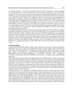
Figure 5 shows the IPCE spectra of the nanostructured TiO
2
electrodes adsorbed with com-
bined CdS/CdSe QDs for different adsorption times, together with that adsorbed with CdS
QDs only. The pre-adsorption time of CdS QD layer is fixed at 40 min. Photoelectrochemical
current in the visible light region due to the adsorbed CdSe QDs can be observed, indicating
the photosensitization by combined CdS/CdSe QDs. With increasing adsorption time, the red-
shift of photoelectrochemical current can be clearly observed, implying the growth of CdSe
QDs. The IPCE peak value increases with the increase of adsorption time up to 8 hours (~
75%), then decreases until 24 h adsorption owing to the increase of recombination centers or
interface states, together with the decrease of energy difference between LUMO in CdSe QDs
and the bottom of conduction band of TiO
2
. Also, the comparison between the adsorption of
CdSe QDs on the TiO
2
electrodes with and without a pre-adsorbed CdS QD layer was carried
out to evaluate the difference in IPCE spectra. For that, Figure 5 shows the IPCE spectra of the
nanostructured TiO
2
electrodes adsorbed with CdSe QDs without a pre-adsorbed layer of CdS
QD layer for different adsorption times. Photoelectrochemical current in the visible light
region due to the adsorbed CdSe QDs can be observed in Fig. 6, also indicating the
photosensitization by CdSe QDs. With increasing adsorption time, the red-shift of
photoelectrochemical current can be clearly observed, implying the growth of CdSe QDs.
However, the appearance of the spectrum in Fig. 6 is different from that of combined
CdS/CdSe QDs, namely in the reduction of maximum IPCE value (~ 60%) and the adsorption
time dependence of the spectrum shape. Also, the IPCE spectra below the CdSe QDs
adsorption time of 8 h agree with that of pure nanostructured TiO
2
electrode within the
experimental accuracy, indicating that the CdSe QDs adsorbed on the nanostructured TiO
2
electrode without a pre-adsorbed CdS layer show very slow growth or no growth similar to
the results of PA characterization in Fig. 3. These results demonstrate that the spectral
response of IPCE is enhanced upon combined CdS/CdSe sensitization rather than single CdSe
QDs sensitization, indicating the possibility of the reduction in recombination centers and
interface states owing to the possibilities of active CdSe QDs by the excess Cd remaining after
CdS adsorption and passivation effect of CdS QDs on the nanostructured TiO
2
surface.
Optical Absorption and Photocurrent Spectra of CdSe Quantum
Dots Adsorbed on Nanocrystalline TiO
2
Electrode Together with Photovoltaic Properties
483
Fig. 5. IPCE spectra of nanostructured TiO
2
electrodes adsorbed with CdS/CdSe quantum dots
for different adsorption times together with that adsorbed with CdS quantum dots only.
Fig. 6. IPCE spectra of nanostructured TiO
2
electrodes adsorbed with CdSe quantum dots
without a preadsorbed CdS QD layer for different adsorption times.
The photocurrent-voltage cureves of (a) combined CdS/CdSe QD- and (b) CdSe QD-
sensitized solar cells are shown in Fig. 7 (a) and (b), respectively, for different adsorption
times, together with that obtained with cells adsorbed with CdS only. However, the
Solar Cells – New Aspects and Solutions
484
appearance of the current-voltage curves of combined CdS/CdSe QD-sensitized solar cells
is different from those of CdSe QD-sensitized solar cells. Figure 8 and 9 illustrates the
photovoltaic parameters ((a) J
sc
; (b) V
oc
; (c) FF; (d) η) of combined CdS/CdSe QD-sensitized
(●) and CdSe QD-sensitized (○) solar cells as a function of CdSe QDs adsorption times.
Fig. 7. Photocurrent-voltage curves of (a) combined CdS/CdSe quantm dot- and (b) CdSe
quantum dot-sensitized solar cells for different adsorption times together with that
adsorbed with CdS quantum dots only.
We observe that the parameter of J
sc
in combined CdS/CdSe QD-sensitized solar cells
increases with the increase of CdSe QDs adsorption times up to 8 h. On the other hand, V
oc
and FF are independent of adsorption times. The performance of solar cells improved with
Optical Absorption and Photocurrent Spectra of CdSe Quantum
Dots Adsorbed on Nanocrystalline TiO
2
Electrode Together with Photovoltaic Properties
485
an increase in adsorption time up to 8 h due, mainly, not only to the increase of the amount
of CdSe QDs but the improvement in crystal quality and decrease of interface states.
However, the increase in adsorption times after more than 8 h leads to deterioration in J
sc
and
V
oc
. High adsorption time of CdSe QDs might cause an increase in recombination centers, poor
penetration of CdSe QDs, and the decrease of energy difference between LUMO in CdSe QDs
and the bottom of conduction band of TiO
2
. Therefore, η of the combined CdS/CdSe QD-
sensitized solar cell shows a maximum of 3.5% at 8 h adsorption times. On the other hand, J
sc
and η below the CdSe QDs adsorption time of 8 h without a pre-adsorbed CdS layer show
very small values close to zero, indicating the very small amount of CdSe QDs adsorption
similar to the results of PA and IPCE characterization. We can observe that J
sc
, V
oc
, FF, and η in
Fig. 8. Dependence of the photovoltaic parameters ((a) J
sc
and (b) V
oc
) on the adsorption
time, both of combined CdS/CdSe (●) and CdSe without a preadsorbed CdS QD layer (○).
Solar Cells – New Aspects and Solutions
486
Fig. 9. Dependence of the photovoltaic parameters( (c) FF and (d) η ) on the adsorption time,
both of combined CdS/CdSe (●) and CdSe without a preadsorbed CdS QD layer (○).
CdSe QD-sensitized solar cells without a pre-adsorbed CdS QD layer increase with the
increase of adsorption times up to 24 h, indicating the difference of the crystal growth and the
formation of recombination centers in combined CdS/CdSe and CdSe QDs.
Figure 9 shows the preliminary ultrafast photoexcited carrier dynamics characterization of
combined CdS/CdSe and CdSe without a pre-adsorbed CdS layer (average diameters of
both CdSe QDs are ~ 6 nm) using a improved transient grating (TG) technique (Katayama et
al., 2003; Yamaguchi et al., 2003; Shen et al., 2010). TG signal is proportional to the change in
the refractive index of the sample due to photoexcited carriers (electrons and holes). TG
method is a powerful time-resolved optical technique for the measurements of various
kinds of dynamics, such as carrier population dynamics, excited carrier diffusion, thermal
Optical Absorption and Photocurrent Spectra of CdSe Quantum
Dots Adsorbed on Nanocrystalline TiO
2
Electrode Together with Photovoltaic Properties
487
diffusion, acoustic velocity and so on. Improved TG technique features very simple and
compact optical setup, and is applicable for samples with rough surfaces. Comparing with
transient absorption (TA) technique, improved TG method has higher sensitivity sue to its
zero background in TG signals, which avoids the nonlinear effect and sample damage.
Figure 9 shows that the hole and electron relaxation times of nanostructured TiO
2
electrodes
adsorbed with combined CdS/CdSe QDs are faster about twice than those with CdSe QDs
without a pre-adsorve CdS layer, indicating the decreases in recombination centers.
Fig. 10. Ultrafast carrier dynamics of combined CdS/CdSe and CdS without preadsorbed
CdS quantum dots layer with a transient grating (TG) technique.
4. Conclusion
We have described the performance of quantum dot-sensitized solar cells (QDSCs) based on
CdSe QD sensitizer on a pre-adsorbed CdS layer (combined CdS/CdSe QDs) together with the
basic studies of optical absorption and photoelectrochemical current characteristics. It can be
observed from optical absorption measurements using photoacoustic (PA) spectroscopy that
the CdSe QDs on the nanostructured TiO
2
electrodes with a pre-adsorbed CdS layer grow
more rapidly during the initial adsorption process than those without a pre-adsorbed CdS
layer. Photoelectrochemical current in the visible light region due to the adsorbed CdSe QDs
can be observed, indicating the photosensitization by combined CdS/CdSe QDs. The
maximum IPCE value (~ 75%) of the CdSe QDs on the nanostructured TiO
2
electrodes with a
pre-adsorbed CdS QD layer is 30% greater than that without a pre-adsorbed CdS layer. It
indicates the possibilities of a decrease in recombination centers, interface states, and inverse
transfer rate that is suggested by the preliminary ultrafast photoexcited carrier carrier
dynamics characterization owing to the possibilities of active CdSe QDs by the excess Cd
remaining after CdS adsorption and passivation effect of CdS QDs on the nanostructured TiO
2
surface. The short-circuit current (J
sc
) in combined CdS/CdSe QD-sensitized solar cells shows
Solar Cells – New Aspects and Solutions
488
maxima with the increase of CdSe QDs adsorption times between 2 h and 24 h, also indicating
the decrease of recombination centers, interface states, and the increase in quasi Fermi level.
The open-circuit voltage (V
oc
) and fill factor (FF) are independent of adsorption times. The
photovoltaic conversion efficiency (η) of the combined CdS/CdSe QD-sensitized solar cell
shows a maximum value of 3.5%.
5. References
Bawendi, M. G.; Kortan, A. R.; Steigerwals, M.; & Brus, L. E. (1989), J. Chem. Phys., Vol. 91, p. 7282.
Chiba, Y.; Islam, A.; Watanabe, Y.; Koyama, R.; Koide, N.; & Han, L. (2006), Jpn. J. Appl.
Phys.Vol. 43, p. L638.
Diguna, L. J.; Shen, Q.; Kobayashi, J.; & Toyoda, T (2007), Appl. Phys. Lett., Vol. 91, p. 023116.
Giménez, S; Mora-Seró, I; Macor, L.; Guijarro, N.; Lala-Villarreal, T.; Gómez, R.; Diguna,
L.;Shen, Q.; Toyoda, T; & Bisquert, J (2009), Nanotechnology, Vol. 20, p. 295204.
Gorer, S.; & Hodes, G. (1994), J. Phys. Chem., Vol. 98, p. 5338.
Hines, M. A.; & Sionnet, P. G. (1996), J. Phys. Chem., Vol. 100, p. 468.
Hodes, G; Manassen, J; & Cahen, D. (1980), J. Electrochem. Soc., Vol. 127, p. 544.
Inoue, Y.; Toyoda, T; & Morimoto, J (2006), Jpn. J. Appl. Phys., Vol. 45, p. 4604.
Jayakrishnan, R.; Nair, J. P.; Kuruvilla, B. A.; & Pandy, R. K. (1996) Semicond. Sci. Tech., Vol.
11, p. 116.
Katayama, K.; Yamaguchi, M.; & Sawada, T. (2003), Appl. Phys. Lett., Vol. 82, p. 2775.
Klimov, V. I. (2006), J. Phys. Chem. B, Vol. 110, p. 16827.
Lee, Y-L.; & Lo, Y-S. (2009), Adv. Func. Mater., Vol. 19, p. 604.
Mora-Seró, I; Giménez, S; Fabregat-Santiago, F.; Gómez, R.; Shen, Q.; Toyoda, T; & Bisquert,
J. (2009), Acc. Chem. Res., Vol. 42, 1848.
Niitsoo, O.; Sarkar, S. K.; Pejoux, P.; Rühle, S.; Cahen, D.; & Hodes, G., J. Photochem.
Photobiol. A, Vol. 182, 306.
Nozik, A. J. (2002), Physica E, Vol. 14, p. 16827.
O’Regan, B.; & Grätzel (1991), Nature, Vol. 353, p. 737.
Rosencwaig, A. & Gersho, A. (1977), J. Appl. Phys., Vol. 47, p. 64.
Schaller, R. D.; Sykora, M.; Pietryga, J. M.; & Klimov, V. I. (2006), Nono Lett., Vol. 6. P. 424.
Shen, Q.; & Toyoda, T (2004), Jpn. J. Appl. Phys., Vol. 43, p. 2946.
Shen, Q.; Arae, D.; & Toyoda, T. (2004), J. Photochem. Photobiol. A, Vol. 164, p. 75
Shen, Q.; Kobayashi, J.; Doguna, L. J.; & Toyoda, T. (2008), J. Appl. Phys., Vol. 103, p. 084304.
Shen, Q.; Ayuzawa, Y.; Katayama, K.; Sawada, T.; & Toyoda, T. (2010), Appl. Phys. Lett.,
Vol. 97, p. 263113.
Shockley, W.; & Queisser, H. J. (1961), J. Appl. Phys., Vol. 32, p. 510.
Sudhager, P.; Jung, J. H.; Park, S; Lee, Y-G.; Sathyamamoorthy, R.; Kang, Y. S.; & Ahn,
H.(2009), Electrochem. Commun., Vol. 11, p. 2220.
Tam, A. C. (1986), Rev. Mod. Phys., Vol. 58, p. 381.
Toyoda, T.; Uehata, T.; Suganuma, R.; Tamura, S; Sato, A; Yamamoto, K.; Shen, Q. &
Kobayashi, N. (2007), Jpn. J. Appl. Phys., Vol. 46, p. 4616.
Toyoda, T; Tsugawa, S.; & Shen, Q. (2009), J. Appl. Phys., Vol. 105, p. 034314.
Trinh, M. T.; Houtepen, A. J.; Schints, J. M; Hanrath, T.; Piris, J.; Knulst, W.; Goossens, P. L.
M.; & Siebbeles, L. D. A. (2008), Nano Lett, Vol. 8, p. 1713
Yamaguchi, M.; Katayama, K.; & Sawada, T. (2003), Chem. Phys. Lett., Vol. 377, p. 589.
Underwood, D. F.; Kippeny, T.; & Rosenthal, S. J. (2001), Eur. Phys, J. D, Vol. 16, p. 241.
Yang, S. M.; Huang, C. H.; Zhai, J.; Wang, Z. S.; & Liang, L. (2002), J. Mater. Chem., Vol.
12,p. 1459.
23
Investigation of Lattice Defects in GaAsN
Grown by Chemical Beam Epitaxy Using
Deep Level Transient Spectroscopy
Boussairi Bouzazi
1
, Hidetoshi Suzuki
2
, Nobuaki Kijima
1
,
Yoshio Ohshita
1
and Masafumi Yamaguchi
1
1
Toyota Technological Institute
2
Myazaki University
Japan
1. Introduction
With only 3 % of N and 9 % of In, InGaAsN with a band gap of 1.04 eV was obtained and
could be lattice matched to GaAs and Ge. This dilute nitride semiconductor has been
selected as a promising candidate for high efficiency multijunction tandem solar cells (Geisz
and Friedman, 2002). However, the diffusion length of minority carriers and the mobility are
still lower than of that in GaAs or InGaAs and showed a considerable degradation with
increasing the N concentration. These electrical properties are insufficient to insure the
current matching in the multijunction solar cell structure AlInGaP/GaAs/InGaAsN/Ge
(Friedman et al., 1998). An obvious reason of such degradation is the high density of N-
related lattice defects that can be formed during growth to compensate for the tensile strain
caused by the small atomic size of N compared with that of arsenic (As) and to the large
miscibility of the gap between GaAs and GaN. These defect centers are expected to act as
active recombination and/or scattering centers in the forbidden gap of the alloy (Zhang &
Wei, 2001). However, no experimental evidence has yet been reported. On the other hand,
the conductivity of undoped p-type InGaAsN or GaAsN and their high background doping
(Friedman et al., 1998; Kurtz et al., 1999; Moto et al., 2000; Krispin et al., 2000) prevent the
design of wide depletion region single junction solar cell and the fabrication of intrinsic
layer to overcome the short minority carrier lifetime. This serious problem was expected in
the first stage to the density of unintentional carbon in the film (Friedman et al., 1998; Kurtz
et al., 1999; Moto et al., 2000). However, the carrier density in some InGaAsN
semiconductors was found to be higher than that of carbon (Kurtz et al., 2002). Furthermore,
the high density of hydrogen (up to 10
20
cm
−3
) and the strong interaction between N and H
in InGaAsN to form N-H related complex were confirmed to be the main cause of high
background doping in InGaAsN films (Li et al., 1999; Janotti et al., 2002, 2003; Kurtz et al.,
2001, 2003; Nishimura et al., 2007). In addition, N-H complex was found theoretically to
bind strongly to gallium vacancies (V
Ga
) to form N-H-V
Ga
with a formation energy of 2 eV
less than that of isolated V
Ga
(Janotti et al., 2003). These predictions were supported
experimentally using positron annihilation spectroscopy results (Toivonen et al., 2003).
Solar Cells – New Aspects and Solutions
490
On the other hand, similar electrical properties were obtained in InGaAsN grown by metal-
organic chemical vapor deposition (MOCVD) and molecular beam epitaxy (MBE) despite
the large difference in the density of residual impurities, which excludes them as a main
cause of low mobilities and short minority carrier lifetimes. For that, lattice defects,
essentially related to the N atom, were expected to be the main reason of such degradation.
Several theoretical and experimental studies have investigated carrier traps in InGaAsN
films. Theoretically, using the first principles pseudo-potential method in local density
approximation, four N-related defects were proposed: (As
Ga
-N
As
)
nn
, (V
Ga
-N
As
)
nn
, (N-N)
As
,
and (N-As)
As
( Zhang & Wei, 2001). While the two first structures were supposed to have
lower formation probabilities, the two split interstitials (N-N)
As
, and (N-As)
As
were
suggested to compensate the tensile strain in the film and to create two electron traps at
around 0.42 and 0.66 eV below the conduction band minimum (CBM) of InGaAsN with a
band gap of 1.04 eV, respectively (Zhang & Wei, 2001). Experimentally, the ion beam
analysis provided a quantitative evidence of existence of N-related interstitial defects in
GaAsN (Spruytte et al., 2001; Ahlgren et al., 2002; Jock, 2009). Furthermore, several carrier
traps were observed in GaAsN and InGaAsN using deep level transient spectroscopy
(DLTS). A deep level (E2/H1), acting as both an electron and a hole trap at 0.36 eV below
the CBM, was observed (Krispin et al., 2001). Other electron traps in GaAsN grown by MBE
were recorded: A2 at 0.29 eV and B1 at 0.27 eV below the CBM of the alloy (Krispin et al.,
2003). In addition, a well known electron trap at 0.2 0.3 eV and 0.3 0.4 eV below the CBM
of p-type and n-type GaAsN grown by MOCVD were observed, respectively (Johnston et al.,
2006). Although the importance of these results as a basic knowledge about lattice defects in
GaAsN and InGaAsN, no recombination center was yet experimentally proved and
characterized. Furthermore, the main cause of high background doping in p-type films was
not completely revealed.
Chemical beam epitaxy (CBE) has been deployed (Yamaguchi et al., 1994; Lee et al., 2005) to
grow (In)GaAsN in order to overcome the disadvantages of MOCVD and MBE. It combines
the use of metal-organic gas sources and the beam nature of MBE. (In)GaAsN films were
grown under low pressure and low temperature to reduce the density of residual impurities
and to avoid the compositional fluctuation of N, respectively. Furthermore, a chemical N
compound source was used to avoid the damage of N species from N
2
plasma source in
MBE. Although we obtained high quality GaAsN films gown by CBE, the diffusion length of
minority carriers is still short (Bouzazi et al., 2010). This indicates that the electrical
properties of GaAsN and InGaAsN films are independent of growth method and the
problem may be caused by the lattice defects caused by N. Therefore, it is necessary to
investigate these defects and their impact on the electrical properties of the film. For that,
this chapter summarizes our recent results concerning lattice defects in GaAsN grown by
CBE. Three defect centers were newly obtained and characterized. The first one is an active
non-radiative N-related recombination center which expected to be the main cause of short
minority carrier lifetime. The second lattice defect is a N-related acceptor like-state which
greatly contributes in the background doping of p-type films. The last one is a shallow
radiative recombination center acceptor-like state.
2. Deep level transient spectroscopy
To characterize lattice defects in a semiconductor, several techniques were used during the
second half of the last century. Between these methods, we cite the thermally stimulated
Investigation of Lattice Defects in GaAsN
Grown by Chemical Beam Epitaxy Using Deep Level Transient Spectroscopy
491
current (TSC) (Leonard & Grossweiner, 1958; Bube, 1960), the admittance spectroscopy
(Losee, 1974), the increase or decay curves of photoconductivity (Rose, 1951; Devore, 1959),
the optically stimulated conductivity (Lambe, 1955; Bube, 1956), and the analysis of space-
charge-limited currents as function of applied voltage (Smith & Rose, 1955; Rose, 1955;
Lampert, 1956). The basic concept of using the change of capacitance under bias conditions
by the filling and emptying of deep levels was already anticipated fifty years ago (Williams,
1966). The thermally stimulated capacitance (TSCAP), which gives the temperature
dependence of junction capacitance (Sah et al., 1978; Sah & Walker, 1973), was used. By
dressing the properties of all these techniques, D. V. Lang found that they lacked the
sensitivity, the speed, the depth range of recorded trap, and the spectroscopic nature to
make them practical for doing spectroscopy on non-radiative centers. For that, in 1974, he
proposed DLTS as a characterization method of lattice defects that can overcome the
disadvantages of the other methods (Lang, 1974). DLTS is based on the analysis of the
change of capacitance due to a change in bias condition at different temperatures. It can be
applied to Schottky contacts and p-n junctions. DLTS has advantages over TSC due to its
better immunity to noise and surface channel leakage currents. It can distinguish between
majority and minority carrier traps, unlike TSC, and has a strong advantage over admittance
spectroscopy, which is limited to majority-carrier traps. Comparing with TSCAP, DLTS has
much greater range of observable trap depths and improved sensitivity. Despite the success
of optical techniques such as photoluminescence to characterize superficial levels, they are
rarely used in the study of non-radiative deep levels. Furthermore, such experiences must
be done in the infrared domain. However, sensors are less sensitive than in the visible
domain. Thus, we need a technique, which can separate between minority and majority
traps and evaluate their concentrations, their energies, and their capture cross sections.
2.1 Fundamental concept of DLTS
2.1.1 Capacitance transient
To fully understand DLTS, it is worth to have a basic knowledge of capacitance transients
arising from the SCR of Schottky contacts or p
+
-n/n
+
-p asymmetric junctions. If a pulse
voltage is applied to one of these device structures that is originally reverse-biased, the SCR
width decreases and the trap centers are filled with carriers (majority or minority depending
on the structure). When the junction is returned to reverse bias condition, the traps that
remains occupied with carriers are emptied by thermal emission and results in a transient
decay. The capacitance transients provide information about these defect centers. Here, we
restrain our description to a p
+
-n junction where the p-side is more much heavily doped
than the n-side, which gives the SCR almost in the low doped side.
The causes of change in capacitance depend on the nature of applied voltage. In case of
reverse biased voltage, the junction capacitance, due to the change in SCR width, is
dominant. However, when the applied voltage is forward biased, the diffusion capacitance,
due to the contribution of minority carrier density, is dominant. The basic equation
governing the capacitance transient in the p
+
-n junction is expressed by
DT T
Rb D D
eN N t N t
Ct A C
VV N N
0
0
() 1exp 1exp
2( ) 2 2
(1)
where A is the contact area, V
b
is the built-in potential,
0
is the permittivity of the
semiconductor material, and e is the elementary charge of an electron. C
0
, N
T
, N
D
, and
Solar Cells – New Aspects and Solutions
492
denote the junction capacitance at reverse bias, the density of filled traps under steady state
conditions, the ionized donor concentration, and the time constant that gives the emission
rate, respectively. The change in capacitance after the recharging of traps is given by
T
D
N
CC
N
0
1
(2)
In most cases of using transient capacitance, the trap centers form only a small fraction of
the SCR impurity density, i.e., N
T
<< N
D
. Hence, using a first-order expansion of Eq. (2)
gives
TD TD
CC NNCNN
00
12 2
(3)
Thus, the trap concentration calculates from the capacitance change C is expressed by
TD
C
NN
C
0
2
(4)
Note that Eq. (3) assumes that N
T
<< N
D
and the traps are filled throughout the total
depletion width. To be more accurate, N
T
should be adjusted to N
Tadj
according to [30]
R
Tadj D
CW
NN
CLL
2
22
012
2
(5)
where W
R
is the total SCR at reverse bias voltage V
R
, L
1
= W
R
- , L
2
= W
p
- , and
FT
D
EE
eN
12
0
2
2
(( ))
(6)
where W
p
, E
F
, and E
T
denote the SCR at V
p
, the Fermi level, and the trap energy level.
2.1.2 Thermal emission of carriers from deep levels
The emission rates for electrons and holes are given, respectively by
CBM T
nnthnc
EE
evN
kT
exp (7)
TVBM
ppthpv
EE
evN
KT
exp (8)
where
n
, N
c
, and v
thn
are the thermal capture cross section, the density of states, and the
thermal velocity of holes, respectively.
p
, N
v
, and v
thp
are the same parameters for holes.
E
CBM
, E
VBM
, and E
T
are the energy levels of the conduction band minimum, the valence band
maximum, and the trap, respectively.
2.2 Other DLTS related techniques
The isothermal capacitance transient spectroscopy (ICTS) and the double carrier pulse DLTS
(DC-DLTS) are two DLTS related methods. They are used to obtain the density profiling of
lattice defects and to check whether they act as recombination centers or not, respectively.
Investigation of Lattice Defects in GaAsN
Grown by Chemical Beam Epitaxy Using Deep Level Transient Spectroscopy
493
2.2.1 Isothermal capacitance transient spectroscopy
ICTS is used to analyze the profiling of lattice defects in the SCR of the semiconductor. It can
be done through three different methods. The first one is obtained by fixing V
R
and varying V
p
to build difference of transients among the SCR of the device. The second method is evaluated
by measuring at constant V
p
and varying V
R
. The last option is obtained by varying V
R
and V
p
,
where the profiling analysis is also possible without building difference of transients. Using
the first method, the medium trap density
T
ij
Nx()
at a point
i
j
x is given by
ij
D
T
ij
RPiPj
C
NA
Nx
CLL
22
0
322
2 ( )
()
()
(9)
where C
ij
is the amplitude difference of the two capacitance transients.
2.2.2 Double carrier pulse DLTS
DC-DLTS is used in asymmetric n
+
-p or p
+
-n junctions (Khan et al., 2005). It aims to check
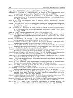
whether a trap is a recombination center or not. As shown in Fig. 1, two pulsed biases are
applied to the sample, in turn, to inject majority and minority carriers to an electron trap. At
the initial state, the junction is under reverse bias, and the energy level E
T
of the trap is
higher than the Fermi level (E
Fn
).When the first pulse voltage is applied to the sample, E
Fn
is
higher than E
T
, which allows the trap to capture electrons. During the second reverse biased
pulse, with a duration t
ip
, holes are injected to the SCR from the pside of the junction. After
the junction pulse is turned off, electrons and holes are thermally emitted. The amount of
trapped carriers can be observed as a change in the DLTS peak height of the trap. If the trap
captures both electrons and holes, the DLTS maximum of the corresponding level decreases
compared with that in conventional DLTS. Such a decrease is explained by the electronhole
(e
h) recombination process, which indicates that the level is a recombination center.
Fig. 1. Basic concept of capture and thermal emission processes from an electron trap located
at an energy level E
T
in p
+
-n junction. A saturating injection pulse is applied to the reverse
biased junction to fill the trap with holes.
V
ip
V
R
t
p
t
ip
V
p
0
(1)Quiescent
reverse bias
(2) Majority
carriers’ in
j
ection
(3) Minority carriers’
in
j
ection
(4)Beginning of
thermal emission
p
+
n
p
+
n
p
+
n
p
+
n
Solar Cells – New Aspects and Solutions
494
To formulate the recombination process, we consider the same notation in § 2.1.2, with
assuming that n
N
D
. The relationship between the total density of recombination centers
and that only occupied by electrons in the n-side of the junction can be expressed by
( ) [ ( )] ( ) [ ( )]
T
pT p T T DnT n T T
dn
ent pcN nt Ncnt eN nt
dt
(10)
where p is the average of injected holes. As a solution of Eq. (10), we have
() ()[(0)-()]exp(- )
ip
T
Tip T T T
t
dn
nt n n n
dt
(11)
where n
T
() = (pc
p
+ e
n
)/(
-1
N
T
),
-1
= pc
p
+ N
D
c
n
+
e
n
+ e
p
), and t
ip
is the width of the injected
pulse. Considering the I
DLTS
and I
DC-DLTS
the peak heights of the recombination center in
conventional and DC-DLTS, respectively. Equation (11) can be rewritten properly as
ip
()
T
DLTS DCDLTS
p
thp ip
TDCDLTS
nt
II
p
vt
NI
(12)
Similarly for hole trap in the p-side of a n
+
-p junction, which acts as recombination center,
we obtain
ip
()
T
DLTS DCDLTS
nthnip
TDCDLTS
nt
II
nvt
NI
(13)
where n is the average of injected electrons.
3. Experimental procedure
All GaAsN films were grown by CBE on high conductive n- or p-type GaAs 2 off toward
[010] substrate using Triethylgallium ((C
2
H
5
)
3
Ga, TEGa), Trisdimethylaminoarsenic
([(CH
3
)
2
N]
3
As, TDMAAs), and Monomethylhydrazine (CH
3
N
2
H
3
, MMHy) as Ga, As, and N
sources, respectively. The flow rates TEGa = 0.1 sccm and TDMAAs = 1.0 sccm were
considered as conventional values. The growth temperatures of 420 C and 460 C were
used for p-type and n-type GaAsN, respectively. Concerning the doping, p-type GaAsN
films are unintentionally doped. The n-type alloys were obtained using a silane (SiH
4
)
source or by growing the films under lower MMHy and high growth temperature.
Three different device structures are used in this study: (i) n- and p-type GaAsN schottky
contacts, (ii) n
+
-GaAs/p-GaAsN/p-GaAs, and (iii) n-GaAsN/p
+
-GaAs hetro-junctions. The N
concentration in all GaAsN layers was evaluated using XRD method. Aluminum (Al) dots
with a diameter of 0.5/1 mm were evaporated under vacuum on the surface of each sample.
Alloys of Au-Ge (88:12 %) and Au-Zn (95:05 %) were deposited at the bottom of n-type and
p-type GaAs substrates for each device, respectively. Some samples were treated by post-
thermal annealing under N
2
liquid gas and using GaAs cap layers to avoid As evaporation
from the surface. The temperature and the time of annealing will be announced depending
on the purpose of making annealing. The background doping and the doping profile in the
extended depletion region under reverse bias condition were evaluated using the
capacitance-voltage (C-V) method. The leakage current in all used samples ranged from 0.3
Investigation of Lattice Defects in GaAsN
Grown by Chemical Beam Epitaxy Using Deep Level Transient Spectroscopy
495
nA to 10
A for a maximum reverse bias voltage of -4 V. A digital DLTS system Bio-Rad
DL8000 was used for DLTS and C-V measurements. The activation energy E
t
and the
capture cross section
n,p
were determined from the slope and the intercept values of the
Arrhenius plot, respectively.
4. Lattice defects in GaAsN grown by CBE
In this section, the distribution of electron and hole traps in the depletion region of GaAsN
grown by CBE will be dressed using DLTS and related methods.
4.1 Electron traps in GaAsN grown by CBE
4.1.1 DLTS spectra and properties of a N-related electron trap
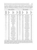
The DLTS spectrum of Fig. 2(a) shows an electron trap (E2) at 0.69 eV below the CBM of GaAs.
After rapid thermal annealing at 720C for 2 min, E2 disappears completely whereas a new
electron trap (E3) appears at 0.34 eV below the CBM. From the Arrhenius plots of Fig. 2(d), the
capture cross sections of E2 and E3 are calculated to be
E2
= 8.1 × 10
-15
cm
2
and
E3
= 7.5 × 10
-18
cm
2
, respectively. Based on previous results about native defects in n-type GaAs,
E2 and E3 are independent of N and considered to be identical to EL2 and EL3, respectively
(Reddy et al., 1996). In order to focus only on N-related lattice defects, these two energy levels
will be excluded from the DLTS spectra of Ncontaining n-type GaAsN. The addition
100 150 200 250 300
0.0
3.4
6.8
Annealed
E2
DLTS signal (arb. unit)
Temperature (K)
E3
x3
(a)
100 150 200 250 300
0.0
0.1
0.2
0.3
0.4
0.5
Tempertaure (K)
DLTS Signal (arb. unit)
As grown
E1
E2
(b)
100 150 200 250 300
0.00
0.05
0.10
0.15
Tempertaure (K)
DLTS Signal (arb. unit)
Annealed
E1
E3
(c)
3.6 5.4 7.2
54.6
56.7
58.8
E1
E3
Ln.v
th
.N
c
)
1000/T (1/K)
E2
(d)
Fig. 2. DLTS spectra of (a) N free as grown and annealed GaAs, (b) as grown n-type
GaAs
0.998
N
0.002
, (c) annealed n-type GaAs
0.998
N
0.002
, and (d) Arrhenius plots of DLTS
spectra.
Solar Cells – New Aspects and Solutions
496
of a small atomic fraction of N to GaAs leads to the record of a new electron trap (E1), at an
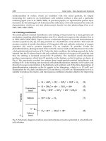
average activation energy 0.3 eV below the CBM of GaAsN. The DLTS spectra of as grown
and annealed n-type GaAs
0.998
N
0.002
are given in Figs. 2. (b) and (c), respectively. The
activation energies (E
E1
) and the capture cross sections (
E1
) of E1 for N varying GaAsN
samples are given Fig. 3 (a) and (b), respectively. The fluctuation of E
E1
from one sample to
another can be explained by the effect of PooleFrenkel emission, where the thermal
emission from E1 is affected by the electric field (Johnston and Kurtz, 2006). As illustrated in
Fig. 3(c), with increasing the filling pulse duration, the DLTS peak height of E1 saturates
0.0 0.1 0.2 0.3 0.4
0.9
1.0
1.1
1.2
1.3
1.4
CBM
As grown
Annealed
Activation energy of E1 (eV)
[N](%)
(a)
0.10.20.30.4
10
-14
10
-13
10
-12
10
-11
As grown
Annealed
Capt. cross sect.
E1
(cm
2
)
[N](%)
(b)
10
-2
10
-1
10
0
0.40
0.45
0.50
0.55
0.60
Peak height of E1 (a. u.)
Filling pulse width tp (s)
Peak saturation
(c)
0.00 0.12 0.24 0.36 0.48
10
15
10
16
10
17
MBE [6]
MOCVD [5]
CBE (annealed)
CBE (as grown)
N
E1
(cm
-3
)
[N] (%)
(d)
60 80 100 120 140
1
10
[N] = 0.036 %
N
E1
profiling (x 10
15
cm
-3
)
Depth (nm)
[N] = 0.212 %
(e)
135 180 225 270
-0.6
-0.3
0.0
DLTS signal (arb. unit)
E2
E1
p-type GaAsN
Temperature (K)
(f)
Fig. 3. Nitrogen dependence of (a) thermal activation energy, (b) capture cross section, and
(d) adjusted density of E1 in as grown and annealed GaAsN samples. The large capture
cross section is confirmed with (c) the filling pulse width dependence of the DLTS peak
height of E1. (e) Density profiling of E1 in the bulk of GaAsN films, and (f) DLTS spectrum
of undoped p-type GaAsN grown by CBE.
Investigation of Lattice Defects in GaAsN
Grown by Chemical Beam Epitaxy Using Deep Level Transient Spectroscopy
497
rapidly. This behavior is explained by the large value of
E1
, compared with that of E2, E3,
and other native defects in GaAs. The adjusted densities of E1 (N
E1
) in as grown and
annealed samples are plotted in Fig. 3(d). N
E1
increases considerably with increasing [N] in
the film and persists to post thermal annealing. This indicates that E1 is a N-related and a
stable electron trap.
The defect center E1 was not observed previously in N free GaAs grown by CBE despite the
existence of N species in the chemical composition of the As source. This can be explained
through three possible scenarios. First, the absence of tensile strain in GaAs prevents the
formation of E1. Second, the N atom in the atomic structure of E1 comes from the N source.
Finally, the N atom comes from the N and As compound sources and in presence of tensile
strain E1 can be formed. The tensile strain was reported in most theoretical and
experimental studies. As given in Fig. 3(e) and using the ICTS, this idea is supported by the
uniform distribution of N
E1
in the bulk of GaAsN. This indicates that E1 is formed during
growth to compensate for the tensile strain in the GaAsN films caused by the small atomic
size of N compared with that of As.
Furthermore, the properties of E1 are identical to that of the famous electron traps reported
by Johnston et Kurtz (Johnston and Kurtz, 2006) and Krispin et al. (Krispin et al., 2003) in
MOCVD and MBE grown ntype GaAsN, respectively. As illustrated in Fig. 3(d), the
densities of these traps are approximately similar to N
E1
despite the large difference in the
density of residual impurities between the three growth methods. Therefore, the atomic
structure of E1 may be free from impurities. Furthermore, by carrying out DLTS
measurements for minority carriers in undoped p-type film, E1 was also observed. This
indicates clearly that E1 is independent of doping atoms (see Fig. 3(f)).
4.1.2 Nature of the electron trap E1
Two methods are used to verify whether E1 is a recombination center or not. The first
method is indirect, in which the activation energy of deep levels is correlated with that of
the reverse bias current in the depletion region of n-type GaAsN Schottky junction and n
+
-
GaAs/p-GaAsN heterojunction. These two device structures are selected because the current
is due mainly to electrons. The second method is direct, in which DC-DLTS is used to show
the behavior of the electron traps in simultaneous injection of majority and minority carriers
in the depletion region.
4.1.2.1 Origin of reverse bias current in GaAsN
The temperature dependence of the reverse bias current in the depletion region of n-type
GaAsN Schottky junction and n
+
-GaAs/p-GaAsN is shown in Fig. 4(a) for reverse bias
voltages of 0.5 and -0.5 V, respectively. At lower temperature, the dark current changes
slowly in the two structures, then fellows an Arrhenius type behavior. As shown in Fig. 4(b),
the same result is obtained by applying reverse bias voltages of 1 and -1 V. Under these
conditions, the reverse bias current I
d
(T) can be expressed by
d
E
IT I
kT
() exp( )
(14)
where I
,
E, k, and T denote the limit of the high-temperature current, the thermal activation
energy of the reverse bias current, the Boltzmann constant, and the temperature, respectively.
The I-V characteristics deviate in the two samples from the thermionic emission. This is
Solar Cells – New Aspects and Solutions
498
explained by the fact that supplying the p-n junction under reverse bias conditions decreases
the product of excess carriers to less than the square of intrinsic carriers. Hence, the Shockley-
Read-Hall (SRH) generation mechanism is activated to increase the product of excess carriers
to assure the balance of charge. The generated carriers are swept to the transition regions by the
electric field in the depletion region. Therefore, an SRH center, with a thermal activation energy
arround 0.3 eV, is the origin of the dark current in the SCR of GaAsN. The thermal activation
energies are measured with respect to majority and minority carriers in n-type GaAsN schottky
junction and n
+
-GaAs/p-GaAsN heterojunction, respectively. This corresponds to the conduction
band in the two structures. By correlating the conduction mechanism and DLTS measurements,
the thermal activation energy of the reverse bias current and the activation energy of the N-
related electron trap E1 are typically identical. Therefore, E1
is responsible for the
generation/recombination current in the depletion region of GaAsN grown by CBE.
36912
10
-11
10
-10
10
-9
10
-8
10
-7
Reverse Bias current |I
d
(A)|
1000/T(K
-1
)
n-type GaAsN
n
+
GaAs/p-GaAsN
(a)
3.08 3.22 3.36 3.50
-16.08
-15.41
-14.74
E
a
= 0.30 eV
n-type GaAsN
Ln(|I
d
(A)|
)
1000/T(K
-1
)
n
+
-GaAs/p-type GaAsN
E
a
= 0.29 eV
(b)
Fig. 4. Temperature dependence of dark current under reverse bias voltages of (a) 0.5 and -
0.5V and (b) 1 and -1V in n-type GaAsN schottky junction and the n
+
-GaAs/p-GaAsN
heterojunction, respectively.
4.1.2.2 DC-DLTS measurements
DC-DLTS is used to confirm the recombination nature of E1 and to characterize the
recombination process via this defect center. An unintentionally doped ntype GaAsN layer
( 1 m) was grown on a ptype GaAs by CBE. This structure is not commonly used for
DLTS measurements. However, the absence of a p-type doping source prevented us to
obtaining a p
+
-n junction. Here, the p-type substrate is used as source of minority carriers. As
shown in Fig. 5(a), the DC-DLTS spectrum is compared with that of the conventional DLTS.
A decrease in the peak height of E1 is observed by varying the voltage of the second injected
pulse and also confirmed by varying its duration. The obvious reason for such reduction is
the mechanism of e-h recombination at the energy level E1 in the forbidden gap of GaAsN.
Hence, E1 is reconfirmed to act as a N-related recombination center. To verify the non-
radiative recombination process, the temperature dependence of
E1
is obtained by varying
the emission rate window e
rw
from 0.5 - 50 s
-1
. The value of
E1
is obtained from the fitting of
the Arrhenius plots for each e
rw
. As shown in Fig. 5(b), the natural logarithmic of
E1
shows a
linear increase with the reciprocal of the temperature. It can be expressed as
Ecape
EkT
1,
ln( )=- ln( )
(15)
where E
cap,e
= 0.13 0.02 eV, k, T, and
= 1.38 x 10
-9
cm
2
denote the barrier height for the
capture of electron, the Boltzmann constant, the temperature, and the capture cross section of
Investigation of Lattice Defects in GaAsN
Grown by Chemical Beam Epitaxy Using Deep Level Transient Spectroscopy
499
electrons at an infinite temperature, respectively. At room temperature,
E1
(300 K) is evaluated
to 8.89 × 10
-12
cm
2
. Such a value is large enough to shorten the lifetime of electrons in p-type
GaAsN. This indicates that E1 is a strongly active recombination center at room temperature
and the e-h recombination process is non-radiative. In addition, from the temperature
dependence of
E1
, the true energy depth of E1 can be obtained by subtracting the barrier
height for electron capture from the thermal activation energy obtained from the Arrhenius
plot. The recombination center E1 is localized at E
a
(E1) = 0.20 0.02 eV from the CBM of
GaAsN. Furthermore, the average capture cross section of holes
p
, at a temperature of T = 175
K, is estimated using Eq. 12 to be
p
(175 K) 5.01 × 10
-18
cm
2
. The physical parameters of E1
can be summarized in a configuration coordinate diagram (CCD), in which the energy state of
E1 is described as a function of lattice configuration (Q). As shown in Fig. 5(c), the CCD of E1
can be presented in three different branches: (i)[0, f.e + f.h]: the charge state of E1 is neutral,
with a free electron and a free hole, (ii)[-, t.e + f.h]: the electron is trapped and the hole remains
free, (iii)[0]: the free hole is captured at the crossed point B and recombined with the already-
trapped electron. E1 losses its charge and becomes neutral. As the recombination process is
non-radiative, the lattice relaxation occurs with the emission of multi-phonon. The energy of
multi-phonon emission can be evaluated as function of N concentration according to
p
honon
g
aca
p
e
ENENEEE
,
() ()((1) )
(16)
150 200 250
0
10
20
30
40
50
E2
2
nd
pulse voltage
(0, -1, -3 V)
DC-DLTS
DLTS signal (x 0.01, arb. unit)
Temperature (K)
E1
(a)
5.0 5.5 6.0 6.5 7.0 7.5
-31.5
-31.0
-30.5
-30.0
-29.5
-29.0
-28.5
-28.0
ln(
E1
(cm
2
))
1000/T(K
-1
)
(b)
Fig. 5. (a) Reduction of peak height of E1 under minority carrier injection spectra, (b)
temperature dependence of
E1
for electrons, and (c) Configuration-coordinate-diagram
showing the different charge states of E1 as function of lattice coordinate parameter.
Lattice coordinate parameter
E(eV)
A
B
E
cap, e
E
th
i
ii
iii
(c)
Solar Cells – New Aspects and Solutions
500
4.1.3 Possible origin of the N-related recombination center E1
It is worth remembering that the atomic structure of E1 may be free from impurities and
doping atoms owing to the difference in the density of residual impurities in GaAsN grown
with MOCVD, MBE, and CBE. Furthermore, the uniform distribution of N
E1
in the bulk of
GaAsN indicates that E1 is formed during growth to compensate for the tensile strain
caused by the small atomic size of N compared with that of As. Therefore, the origin of E1
has high probability to depend only on the atoms of the alloy (N, As, Ga). To confirm these
expectations, the origin of E1 is investigated qualitatively by considering the results of two
different experiments: (i) the dependence of N
E1
to the As source flow rate and (ii) the effect
of H implantation on the distribution of lattice defects in n-type GaAsN.
4.1.3.1 Dependence of N
E1
to As source flow rates
The objective of this experiment is to clarify whether the density of E1 is sensitive to the As
atom or not. The MMHy was supplied to 9.0 sccm and the TDMAAs was varied between
and 0.7 and 1.5 sccm. As shown in Fig. 6. (a), increasing TDMMAs drops the N
concentration in the film and tends to saturate for a flow rate higher than 1 sccm. For two
emission rate e
rw
= {100, 10} s
-1
and filling pulse t
p
= {0.1, 5} ms values, the DLTS spectra are
normalized on the junction capacitance to exclude the effect of various carrier densities in
the samples. The same N-related recombination center E1 was observed in all samples. The
TDMAAs flow rate dependence of the DLTS peak height of E1 for two settings of
measurement parameters is given in Fig. 6(b). A peaking behavior at approximately
TDMAAs = 0.9 sccm was obtained. As N
E1
is uniformly distributed in GaAsN films, the
incorporation of N atom at the growth surface affects both the incorporation of N
As
and the
formation of E1. If E1 depends only on N atom, the decrease of [N] with increasing
TDMMAs flow rate results in monotonically dropping of N
E1
. However, the peaking
behavior of N
E1
indicates the sensitivity of E1 to As atom, either than N.
0.8 1.0 1.2 1.4
0.20
0.25
0.30
[N] (%)
TDMAAS (sccm)
MMHy = 9 sccm
(a)
0.8 1.0 1.2 1.4
1.0
1.5
3.5
4.0
4.5
e
n
=100 s
-1
, t
p
= 0.1ms
C/C
R
(x 10
-3
)
TDMAAs
(
sccm
)
e
n
=10 s
-1
, t
p
= 5.0 ms
(b)
Fig. 6. TDMAAs flow rate dependence of (a) N concentration under supplied MMHy and (b)
normalized DLTS peak height of E1 for two settings of measurement parameters.
4.1.3.2 Effect of H implantation on lattice defects in GaAsN
GaAsN films were treated by H implantation. This experiment was used because H bounds
strongly to N in GaAsN films to form N-H complexes (Suzuki et al., 2008; Amore &
Filippone, 2005). H ions with multi-energy from 10 to 48 keV were implanted into GaAsN
layers with peaks concentration of 5 10
18
(GaAsN
HD1
) and 1 10
19
atom/cm
3
(GaAsN
HD2
),
Investigation of Lattice Defects in GaAsN
Grown by Chemical Beam Epitaxy Using Deep Level Transient Spectroscopy
501
respectively. The depth of implantation was thought to be distributed between 110 and 410
nm from the surface of GaAsN by calculating the SRIM 2003 simulation code (Ziegler, 1985).
After implantation, the samples were treated by post thermal annealing at 500 C for 10 min
under N
2
gas and GaAs cap layers. As plotted in Fig. 7(a) and (b), the crystal quality of
GaAsN films after implantation was controlled using XRD curves and C-V measurements.
DLTS spectra of implanted samples are shown in Fig. 7(c). After implantation, E1 was not
observed; however, two new lattice defects appeared. The signature and the density of these
traps are summarized in Table 1. The thermal emission from them is plotted as an Arrhenius
plot in Fig. 7(d).
GaAsN Traps E
a
(eV)
(cm
2
)
N
t-adj
(cm
-3
) Possible origin
As grown E1 E
CM
-0.331
5.18 10
-15
3.37 10
17
(N-As)
As
Implanted
EP1 E
CM
-0.414
8.20 10
-13
5.88 10
17
EL5 in GaAs
HP1 E
VM
-0.105
5.42 10
-18
1.84 10
16
N-H-V
Ga
Table 1. Summary of E
a
, , adjusted N
t-adj
, and possible origin of defects in as grown and
implanted GaAsN samples.
50 100 150 200
-5
0
5
10
15
20
As grown
GaAsN(HD1)
GaAsN(HD2)
N
t
(x 10
15
cm
-3
)
Temperature (K)
E1
HP1
EP1
(a)
4.5 6.0 7.5 9.0 10.5
49
50
51
52
53
Ln.v
thn
.N
C
)
1000/T
(
1/K
)
HP1
E1
EP1
(b)
Fig. 7. (a)DLTS spectra of as grown and implanted GaAsN and (b) their Arrhenius plots.
The new electron trap (EP1) is located approximately 0.41 eV below the CBM of GaAsN. Its
properties are identical to that of the native defect EL5 in GaAs (Reddy, 1996). Its atomic
structure was discussed in many publications, where the common result indicated that EL5
is a complex defect free from impurities and dominated by As interstitials, such V
Ga
-As
i
or
As
Ga
-V
Ga
(Deenapanray et al., 2000; Yakimova et al., 1993). The second new defect is a hole
trap (HP1) at approximately an average activation energy 0.11 eV above the VBM of GaAsN.
Compared with majority carrier traps in GaAs grown with various techniques, no similar
hole trap to HP1 was reported. However, in p-type GaAsN grown by CBE with around the
same N concentration, E
HP1
and
HP1
are identical to that of the hole trap HC2 in p-type
GaAsN grown by CBE (bouzazi et al., 2011). This defect was confirmed recently to be an
acceptor state in GaAsN films (see § 4.2.3) and to be related to the N-H bond. While the H
impurity was provided by implantation, the N atom can originate through two possibilities:
First; examining XRD results, the N atom can originate from its ideal site. However, [N] in
as grown is much higher than that in implanted samples (10
19
cm
-3
). It is also much higher
than N
HP1
. Second, N atom can be originated from the complete dissociation of E1, since the
Solar Cells – New Aspects and Solutions
502
ratio N
E1
/N
HP1
is less than 2. If E1 is the split interstitial (N-N)
As
, N
HP1
must be at least
equals to that of E1 and one N atom remains free. This expectation is disapproved by DLTS
measurements, where N
HP1
is largely less than N
E1
. This means that E1 contains only one N
atom in its atomic structure. Considering the results of last sub-section, E1 may be the split
interstitial (N-As)
As
formed from one N and one As in a single As site. This result is
supported by the theoretical calculation (Zhang et al., 2001).
4.1.4 Effect of E1 on minority carrier lifetime in GaAsN
The effect of E1 on the electrical properties of GaAsN can be evaluated through the
calculation of minority carrier lifetime using the SRH model for generationrecombination
(Hall, 1952; Shockley & Read, 1952). Such parameter has been estimated to be less than 0.2
ns as a result of the calculation according to
1
111
0.2
EthnEE
v σ Nns
(17)
Therefore, E1 is considered to be the main cause of short minority carrier in GaAsN. It is
required to investigate the formation mechanism of this defect in order to decrease its
density and to recover the minority carrier lifetime in GaAs.
4.2 Hole traps in GaAsN grown by CBE
4.2.1 DLTS spectra and properties of hole traps in GaAsN
Here, we only focus on the hole traps that coexist in all p-type GaAsN based Schottky
junctions and n
+
-GaAs/p-GaAsN heterojunction. The difference between these two
structures is the temperature range in which the DLTS measurements can be carried out due
to the freeze-out of carriers. The DLTS spectrum of p-type GaAsN in the heterojunction is
shown in Fig. 8(a). Three hole traps H0, H2, and H5 are observed at 0.052, 0.185, and 0.662
eV above the VBM of GaAsN. Their peak temperatures are 35, 130, and 300 K, respectively.
The thermal dependence of emission from the hole traps is plotted as an Arrhenius plot in
Fig. 8(b). The activation energy, capture cross section, and density are given in Table 2.
30 35 150 300
0.0
0.5
1.0
1.5
2.0
H5
H2
DLTS signal(a.u)
Temperature (K)
H0
(a)
048242832
51
54
57
H0
H2
Ln(N
v
v
th
.)
1000/T(1/K)
H5
(b)
Fig. 8. (a) DLTS spectra of p-type GaAsN grown by CBE and (b) their Arrhenius plots.
The hole traps H2 and H5 were also observed in Schottky junctions and coexist in all
samples. H2 is a N-related acceptor-like state and was proved to be in good relationship
with high background doping in GaAsN films. These properties will be discussed later. The
Investigation of Lattice Defects in GaAsN
Grown by Chemical Beam Epitaxy Using Deep Level Transient Spectroscopy
503
hole trap H5 presents the same properties as H3 and HA5 (Li et al., 2001; Katsuhata et al.,
1978). It is proposed to be the double donor state (
+
/
++
) of EL2 (Bouzazi et al., 2010). The hole
trap H0 cannot be observed in Schottky junctions owing to the freeze-out effect.
Traps E
t
(eV)
p
(cm
2
)
N
t-adj
(cm
-3
)
H0 0.052
2.16 10
-14
4.64 10
16
H2 0.185
3.87 10
-17
4.52 10
15
H5 0.662
6.16 10
-14
6.24 10
15
Table 2. Summary of E
t
,
p
, and adjusted N
t-adj
of H0, H2, and H5.
4.2.2 Radiative shallow recombination center H0
DC-DLTS measurements were carried out to confirm whether there is a recombination
center among the hole traps or not. As shown in Figs. 9(a) and (b), the DC-DLTS signal is
compared to that of conventional DLTS. A decrease in the DLTS peak height of H0 is
observed and confirmed by varying the voltage and the duration of the injected pulse.
30 35 150 300
0.0
0.5
1.0
1.5
2.0
3.00 V
DC-DLTS
Voltage of the 2
nd
pulse
H3
H2
DLTS signal(a.u)
Tem
p
erature
(
K
)
H0
DLTS
1.75 V
0.0 0.3 0.6 0.9 1.2
0.6
0.9
1.2
1.5
1.8
2.1
DC-DLTS peak height (a. u.)
2
nd
pulse duration (ms)
01234
2
nd
pulse voltage (V)
Fig. 9. (a)DC-DLTS spectra of p-type GaAsN for various second pulse voltage and
(b) H0 DC-DLTS peak height dependence of second pulse voltage and duration.
The shallow hole trap H0 is observed and reported for the first time owing to the
temperature range it was recorded, which cannot be reached with standard DLTS systems.
Second, its capture cross section is large enough to capture majority carriers and minority
carriers. The reduction in the peak height of H0 is explained by the electron hole-
recombination. This implies that H0 is a shallow recombination center in p-type GaAsN
grown by CBE and can also play the role of an acceptor state. To verify whether the
recombination process via H0 is radiative or not, the temperature dependence of the capture
cross section of electrons is obtained by varying the emission rate e
rw
from 1 to 50 s
-1
. As
shown in Fig. 10(a), the peak temperature of H0 shifts to high temperatures with increasing
e
rw
. The value of
H0
is obtained from the fitting of the Arrhenius plots for each e
rw
. It is
important to note that the fitting errors of activation energy and capture cross section are
relatively large owing to the instability of temperature in the range of measurements. As
shown in Fig. 10(b), the capture cross section of H0 does not exhibit an Arrhenius behavior,
which excludes the non-radiative recombination process. Its shallow energy level suggests
Solar Cells – New Aspects and Solutions
504
that H0 plays the role of an intermediate center in the recombination process, with the
exception that the recombination is quite often radiative.
25 30 35 40 45 50 5
5
0.0
0.2
0.4
0.6
0.8
1.0
1.2
1
.
4
DLTS signal (arb. unit)
Temperature (K)
H0
Emission rate window
Peak shift with
(a)
26 28 30 32
10
-18
10
-17
10
-16
10
-15
10
-1
4
Capt. cross sect.
p
(cm
2
)
1000/T
(
1/K
)
(b)
1.26 1.33 1.40
P3
P1
P2
PL intensity (a.u)
Photon Energy (eV)
20k
30k
40k
50k
(c)
20 30 40 50
1.31
1.32
1.38
1.41
P1
P2
Peak Energy (eV)
Temperature (K)
P3
(d)
Fig. 10. (a) Emission rate window dependence of H0 peak, (b) temperature dependence of
capture cross section and activation energy of H0, (c) PL spectra of p-type GaAsN at 20 to 50
K, and (d) temperature dependence of the peaks P1, P2, and P3 obtained from the fitting of
PL spectra.
Furthermore, the capture cross section of electrons can be estimated using Eq. 13 and by the
reduction of the peak height of H0, which follows from the injection of minority carriers. By
varying the injected pulse voltage at fixed duration, the average capture cross section of
electrons
n
, at a temperature T = 35 K, is estimated to be
n
3.64 × 10
-16
cm
2
. However, by
varying the width of the injected pulse at fixed pulse voltage, it is estimated, at the same
temperature, to be
n
3.05 × 10
-16
cm
2
. These two values are nearly identical and indicate
that the capture cross section of electrons and holes of H0 are approximately the same. To
identify this radiative recombination, photoluminescence (PL) measurements were carried
out at low temperature on the same GaAsN sample. The PL spectra at 20, 30, 40, and 50K are
shown in Fig. 10 (c). Three different peaks P1, P2, and P3 can be distinguished from PL
spectra fitting. The temperature dependence of their energies is plotted in Fig. 10 (d). The
three peaks were sufficiently discussed in many N-varying GaAsN samples and they are
proposed to be: (i) P1 is the result of band-to-band transition, (ii) P2 is caused by free exciton
or related to shallow energy level, and (iii) P3 originates from the transition between a
neutral donor and a neutral acceptor pair (DAP) (Inagaki et al., 2011). Therefore, the peak P2
Investigation of Lattice Defects in GaAsN
Grown by Chemical Beam Epitaxy Using Deep Level Transient Spectroscopy
505
is suggested to be in relation with H0. The band diagram of such recombination is shown in
Fig. 11, where the transition occurs between H0 and the CBM and/or a donor-like defect
(E
t
). The transition between free electrons in the CBM and charged H0 is called free-to-
charged bound transition.
Fig. 11. Band diagram of radiative recombination through H0, where the transition occurs
between H0 and the CBM and/or a donor-like defect (E
t
).
Concerning the origin of the acceptor–like hole trap H0, more experiments are required to
discuss it. However, considering its density and the distribution of shallow acceptors in
GaAs, it can be suggested that H0 is a carbon-related acceptor, where the reported ionization
energy from PL and Hall Effect measurements is 0.026 eV and its density in the 10
-15
cm
-3
range (Baldereschi & Lipari, 1974).
4.2.3 Deep N-H related acceptor state H2
The ionized acceptor density (N
A
) is found to be in good linear dependence with N
concentration in p-type GaAsN samples (see Fig. 12 (a)). As given in Figs. 12(b) and (c), the
junction capacitance (C
j
) showed a N-related sigmoid behavior with temperature in the
range 70 to 100 K. This behavior has not yet been observed in GaAs and n-type GaAsN
grown by CBE. It was recorded at 20 K in silicon p-n junction and explained by the
ionization of a shallow energy level (Katsuhata, 1978; 1983). Hence, the N dependence of N
A
and C
j
is explained by the thermal ionization of a N-related acceptor-like state. The thermal
ionization energy of this energy level was estimated in the temperature range 70 to 100 K to
be between 0.1 and 0.2 eV. It is in conformity with the theoretical calculations, which
suggested the existence of a N-related hole trap acceptor-like defect with an activation
energy within 0.03 and 0.18eV above the VBM of GaAsN (Janotti et al., 2003; Suzuki et al.,
2008). Experimentally, a deep acceptor level, A2, was confirmed in CBE grown undoped
GaAsN with ionization energies of E
A1
= 130 ± 20 meV (Suzuki et al., 2008). On the other
hand, the properties of H2 in N-varying GaAsN schottky junctions are cited below: The
peak temperature of H2 is within the temperature range of increase of C
j
. This means that
the electric field at this temperature range fellows the same behavior of C
j
and depends on N
concentration. Hence, the emission of carriers from the charged traps is affect by the Poole-
Frenkel emission (Johnston and Kurtz, 2006). This is confirmed by the fluctuation of E
H2
from one sample to another depending on N concentration (see Table 3). However, the
average of E
H2
is within the energy range of the acceptor level obtained from theoretical
prediction and identical to E
A2
(Suzuki et al., 2008; Janotti et al., 2003). Furthermore, as given
in Fig. 12 (d), N
H2-adj
is in linear dependence with N concentration. Therefore, H2 is proved
to be the N-related hole trap acceptor-like state, which thermal ionization increased C
j
and
E
CBM
E
VBM
E
H0
E
F
E
t
(a)
(b)
E
CBM
E
VBM
E
H0
E
F
E
t
(c)
E
CBM
E
VBM
E
H0
E
F
E
t