Advanced Microwave and Millimeter Wave Technologies Devices, Circuits and Systems Part 7 potx
Bạn đang xem bản rút gọn của tài liệu. Xem và tải ngay bản đầy đủ của tài liệu tại đây (2.29 MB, 40 trang )
AdvancedMicrowaveandMillimeterWave
Technologies:SemiconductorDevices,CircuitsandSystems232
synthesis. It is composed of a divid-by-4/5 dual-modulus prescaler, a divide-by-5 divider,
and a control logic unit. The control logic unit generates the MC signal modulating its
divide rato, and the divide ratio of the four-modulus divider can be set to be 20, 23, 24,
and 25 by varying the duty ratio of the MC signal. And its duty ratio is determined by the
logic values of control bits c
0
and c
1
, as shown in Table of Fig. 10. For example, if c
1
is low
and c
0
is high, the total divide ratio becomes 23; if c
1
is high and c
0
is low, the total divide
ratio becomes 25. Fig. 11 illustrates the timing diagrams of the four-modulus divider. If the
MC signal is low, the divide-by 4/5 prescaler divides the input clock signal by 5. If the
signal MC is high, its divide ratio becomes 4. Therefore, if c
0
is low and c
1
is high, the dual-
modulus prescaler divides the input signal of vco/4 by 4 for two P
o+
cycles and by 5 for
three P
o+
cycles, while the followed divide-by-5 divider swallows five Po+ cycles. Thus, a
total divide ratio (TDR) is calculated as TDR= ( 4) 2 cycles + ( 5) 3 cycles = 23. The
operating timing waveform of the four-modulus divider is illustrated in Fig. 11. Using the
same technique as explained above, the modulus number of the four-modulus divider could
be extended to more numbers of divide ratios.
Fig. 10. Four-modulus divider and its divide ratio
Fig. 11. Operating timing waveform of the four-modulus divider
The implementation of a high-speed prescaler in mixed-signal environment requires careful
attention to certain aspects of the circuit design to contribute low noise to such sensitive
analog circuit as VCO, which shares the same substrate with noisy circuits, and to the
synthesized output signal. Here, both current-mode logic (CML) and ECL-like D-flipflops
instead of a static CMOS logic are used to implement the four-modulus divider. The CML
logic uses constant current source, which generates lower digital noise, and differential
signals at both input and output, which reduce common-mode noise coupled from the
power supply line and substrate because the differential circuit topology does inherently
suppress the common-mode power supply and substrate noise [Park, 1998]. Another issue
of the programmable divider design is reduction in power consumption at a given
frequency range. Most power consumption in divider occurs in the front-end synchronous
4/5 dual-modulus prescaler because it is a part of the circuit operating at the maximum
frequency of the input signal. The 4/5 synchronous dual-modulus prescaler shown in Fig.
12 contains two high-frequency fully functional ECL-like D-flipflops and one ECL-like D-
flipflop with NOR logic. In the dual-modulus prescaler, the outputs of both the second D-
flipflop and the third D-flipflop are feedback into the NOR D-F/F as the control inputs for
generating proper division ratio. The MC signal is given to the third NOR D-F/F for
modulating division ratio. The delay requirement in a critical path of the prescaler loop is
severe because the 4/5 dual-modulus prescaler must operate up to a maximum of 10 GHz.
The operating speed of the prescaler is limited by the delay time of each D-flipflops, and the
prescaler layout. Therefore, the prescaler should be designed and laid out to achieve a delay
time as small as possible and to obtain an operating frequency as high as possible.
Fig. 12. 4/5 dual-modulus prescaler
52-GHzMillimetre-WavePLLSynthesizer 233
synthesis. It is composed of a divid-by-4/5 dual-modulus prescaler, a divide-by-5 divider,
and a control logic unit. The control logic unit generates the MC signal modulating its
divide rato, and the divide ratio of the four-modulus divider can be set to be 20, 23, 24,
and 25 by varying the duty ratio of the MC signal. And its duty ratio is determined by the
logic values of control bits c
0
and c
1
, as shown in Table of Fig. 10. For example, if c
1
is low
and c
0
is high, the total divide ratio becomes 23; if c
1
is high and c
0
is low, the total divide
ratio becomes 25. Fig. 11 illustrates the timing diagrams of the four-modulus divider. If the
MC signal is low, the divide-by 4/5 prescaler divides the input clock signal by 5. If the
signal MC is high, its divide ratio becomes 4. Therefore, if c
0
is low and c
1
is high, the dual-
modulus prescaler divides the input signal of vco/4 by 4 for two P
o+
cycles and by 5 for
three P
o+
cycles, while the followed divide-by-5 divider swallows five Po+ cycles. Thus, a
total divide ratio (TDR) is calculated as TDR= ( 4) 2 cycles + ( 5) 3 cycles = 23. The
operating timing waveform of the four-modulus divider is illustrated in Fig. 11. Using the
same technique as explained above, the modulus number of the four-modulus divider could
be extended to more numbers of divide ratios.
Fig. 10. Four-modulus divider and its divide ratio
Fig. 11. Operating timing waveform of the four-modulus divider
The implementation of a high-speed prescaler in mixed-signal environment requires careful
attention to certain aspects of the circuit design to contribute low noise to such sensitive
analog circuit as VCO, which shares the same substrate with noisy circuits, and to the
synthesized output signal. Here, both current-mode logic (CML) and ECL-like D-flipflops
instead of a static CMOS logic are used to implement the four-modulus divider. The CML
logic uses constant current source, which generates lower digital noise, and differential
signals at both input and output, which reduce common-mode noise coupled from the
power supply line and substrate because the differential circuit topology does inherently
suppress the common-mode power supply and substrate noise [Park, 1998]. Another issue
of the programmable divider design is reduction in power consumption at a given
frequency range. Most power consumption in divider occurs in the front-end synchronous
4/5 dual-modulus prescaler because it is a part of the circuit operating at the maximum
frequency of the input signal. The 4/5 synchronous dual-modulus prescaler shown in Fig.
12 contains two high-frequency fully functional ECL-like D-flipflops and one ECL-like D-
flipflop with NOR logic. In the dual-modulus prescaler, the outputs of both the second D-
flipflop and the third D-flipflop are feedback into the NOR D-F/F as the control inputs for
generating proper division ratio. The MC signal is given to the third NOR D-F/F for
modulating division ratio. The delay requirement in a critical path of the prescaler loop is
severe because the 4/5 dual-modulus prescaler must operate up to a maximum of 10 GHz.
The operating speed of the prescaler is limited by the delay time of each D-flipflops, and the
prescaler layout. Therefore, the prescaler should be designed and laid out to achieve a delay
time as small as possible and to obtain an operating frequency as high as possible.
Fig. 12. 4/5 dual-modulus prescaler
AdvancedMicrowaveandMillimeterWave
Technologies:SemiconductorDevices,CircuitsandSystems234
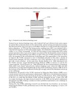
Fig. 13 represents the divider circuit consisting of master-slave D-type latches. They are a
rising edge-triggered E
2
CL D-flipflop with embedded NOR gate and a E
2
CL D-type flipflop,
which are used in the front-end design to achieve a maximum speed and a minimum power.
The master-slave D flipflop is driven by an applied clock signal (CK), and the Q of D-flipflop
changes on each rising edge of the clock. Each latch consists of a differential stage (T
r3
/T
r4
,
T
r7
/T
r8
) for the read-data operation and a cross-coupled stage (T
r1
/T
r2
, T
r5
/T
r6
) for the hold
operation. Both load resistance R
L
and bias current I
L
determine logical swing. There are
four distinct states that the D latch may occupy, representing state transition between
latched and transparent, and on every edge of the clock the D flipflop changes state. To
complete a cycle, all four-state transitions in which both master and slave latches alternate
between transparent and latched states should be carried out in the divider. The maximum
speed of operation of the divider circuit shown in Fig.13 can be determined by the sum of
the delays of each transition. The D latches have two basic operations. The first is a current
steering operation in the T
r9
, T
r10
/T
r11
and T
r12
, T
r13
/T
r14
differential pairs, moving between
latched and transparent settings. The second is a voltage operation that can only occur after
the current steering, changing the output voltage at I and Q nodes. Both of these operations
introduce delay into the divider circuit and limit the maximum operating speed of the
divider. Here, the delay contribution of the master’s transition should be commonly
improved because the master latch shows more slow cycle transition than the slave [Collins,
2005]. Also, in each latch, high-speed operation could be impaired whenever the cross-
coupled stage of each latch failed to accomplish the hold-data phase. Therefore, in the
master-slave D-type flip-flop, the cross-coupled pair with capacitive degeneration (C
d
) is
used for enhancing operation speed. In this case, it can be shown that the input conductance
G() of the cross-coupled pair is negative up to the frequency given by (3).
B
d
T
G
r
CC
f
f
11
2
2
1
0
(3)
Here, C
is base-emitter capacitance of transistor, r
B
is base resistance, and
T
is cut-off
frequency. From (3), the capacitive-degeneration cross-coupled pair has higher conductance-
zero frequency point than the common cross-coupled pair, and hence there is less possibility
to miss the hold-data phase at higher operating frequency. In the capacitive-degeneration
divider, drawbacks such as local instabilities and unwanted oscillations could be expected.
Nevertheless, a careful choice of C
d
and tail current I
L
results in a high free-running
switching time so that oscillations do not start due to the current steering of the bottom
differential pair operating at the input clock frequency [Girlando, 2005]. The method finding
the optimum values of C
d
and I
L
is illustrated in the simulation curves of Fig. 14 through
which their values are set to guarantee both operating speed as high as possible and no
oscillation in the divider. First, the proper value of I
L
should be set within the range of no
oscillation. The Nyquist diagram of Fig. 14(a) shows the divider oscillates above 2.5mA of I
L
,
and then, the tail current is set by 1.5mA in this design considering power and speed. The
clockwise encirclement of 1 at the horizontal axis of the Nyquist polar chart means that the
transfer function of the divider circuit has poles in the right half plane i.e, it oscillates [Paul,
2001][Lee, 2002]. Second, after fixing I
L
, we must check whether the divider oscillates by
sweeping the value of C
d
. As shown in the Nyquist diagram of Fig.14(b), the divider
oscillates over 900f, and the optimum value of C
d
is set to 100fF, considering process
variation and speed. The value of C
d
is the smaller, the higher increases the
G
of Eq. (3).
When C
d
is fixed to 100fF, the conductance zero frequency point of the divider is simulated
by 84GHz, as shown in Fig.14(c)
(a)
(b)
Fig. 13. (a) E
2
CL D-type flipflop with embedded NOR gate (b) E
2
CL D-type flipflop
52-GHzMillimetre-WavePLLSynthesizer 235
Fig. 13 represents the divider circuit consisting of master-slave D-type latches. They are a
rising edge-triggered E
2
CL D-flipflop with embedded NOR gate and a E
2
CL D-type flipflop,
which are used in the front-end design to achieve a maximum speed and a minimum power.
The master-slave D flipflop is driven by an applied clock signal (CK), and the Q of D-flipflop
changes on each rising edge of the clock. Each latch consists of a differential stage (T
r3
/T
r4
,
T
r7
/T
r8
) for the read-data operation and a cross-coupled stage (T
r1
/T
r2
, T
r5
/T
r6
) for the hold
operation. Both load resistance R
L
and bias current I
L
determine logical swing. There are
four distinct states that the D latch may occupy, representing state transition between
latched and transparent, and on every edge of the clock the D flipflop changes state. To
complete a cycle, all four-state transitions in which both master and slave latches alternate
between transparent and latched states should be carried out in the divider. The maximum
speed of operation of the divider circuit shown in Fig.13 can be determined by the sum of
the delays of each transition. The D latches have two basic operations. The first is a current
steering operation in the T
r9
, T
r10
/T
r11
and T
r12
, T
r13
/T
r14
differential pairs, moving between
latched and transparent settings. The second is a voltage operation that can only occur after
the current steering, changing the output voltage at I and Q nodes. Both of these operations
introduce delay into the divider circuit and limit the maximum operating speed of the
divider. Here, the delay contribution of the master’s transition should be commonly
improved because the master latch shows more slow cycle transition than the slave [Collins,
2005]. Also, in each latch, high-speed operation could be impaired whenever the cross-
coupled stage of each latch failed to accomplish the hold-data phase. Therefore, in the
master-slave D-type flip-flop, the cross-coupled pair with capacitive degeneration (C
d
) is
used for enhancing operation speed. In this case, it can be shown that the input conductance
G() of the cross-coupled pair is negative up to the frequency given by (3).
B
d
T
G
r
CC
f
f
11
2
2
1
0
(3)
Here, C
is base-emitter capacitance of transistor, r
B
is base resistance, and
T
is cut-off
frequency. From (3), the capacitive-degeneration cross-coupled pair has higher conductance-
zero frequency point than the common cross-coupled pair, and hence there is less possibility
to miss the hold-data phase at higher operating frequency. In the capacitive-degeneration
divider, drawbacks such as local instabilities and unwanted oscillations could be expected.
Nevertheless, a careful choice of C
d
and tail current I
L
results in a high free-running
switching time so that oscillations do not start due to the current steering of the bottom
differential pair operating at the input clock frequency [Girlando, 2005]. The method finding
the optimum values of C
d
and I
L
is illustrated in the simulation curves of Fig. 14 through
which their values are set to guarantee both operating speed as high as possible and no
oscillation in the divider. First, the proper value of I
L
should be set within the range of no
oscillation. The Nyquist diagram of Fig. 14(a) shows the divider oscillates above 2.5mA of I
L
,
and then, the tail current is set by 1.5mA in this design considering power and speed. The
clockwise encirclement of 1 at the horizontal axis of the Nyquist polar chart means that the
transfer function of the divider circuit has poles in the right half plane i.e, it oscillates [Paul,
2001][Lee, 2002]. Second, after fixing I
L
, we must check whether the divider oscillates by
sweeping the value of C
d
. As shown in the Nyquist diagram of Fig.14(b), the divider
oscillates over 900f, and the optimum value of C
d
is set to 100fF, considering process
variation and speed. The value of C
d
is the smaller, the higher increases the
G
of Eq. (3).
When C
d
is fixed to 100fF, the conductance zero frequency point of the divider is simulated
by 84GHz, as shown in Fig.14(c)
(a)
(b)
Fig. 13. (a) E
2
CL D-type flipflop with embedded NOR gate (b) E
2
CL D-type flipflop
AdvancedMicrowaveandMillimeterWave
Technologies:SemiconductorDevices,CircuitsandSystems236
(a) (b)
(c)
Fig. 14. (a) Nyquist test diagram for oscillation vs I
L
, (b) Nyquist test diagram for oscillation
vs C
d
, (c)
G
simulation vs C
d
, here C
d
= C
v
The CML DFF used in the divide-by-5 circuit is made up of a cascade of a master D-latch
and a slave latch with the clocks reversed in the second ones as shown in Fig. 15. The
differential clocks steer the current of the current source from one side to the other side, and
from the tracking mode to the hold mode. The values of load resistors are set to be as large
as possible to confirm high speed at low current consumption. Transistors such as M1, M2,
M3, and M4 are sized just large enough to be able to completely steer the current at worst
case. Transistors M5 and M6 must be just large enough to quickly regenerate the current
state during the hold mode. Finally, the current magnitude of Is must be high enough to
allow a large swing at the output node and not limit switching bandwidth [Lam, 2000].
Fig. 15. CML D-type flipflop
As static logics require single-ended rail-to-rail swing, the non-rail-to-rail differential swing
of the prescaler must be converted appropriately. A differential-to-single-ended signal level
converter (DSC) must be inserted at the output Q
2
of the CML DFF in figure 10. The simplest
circuit for this task is the four-transistor circuit shown in Fig. 16. The differential outputs of
the CML DFF drive the input PMOS transistors (P1, P2), and then the single-ended output is
at the drains of P2 and N2. P2 charges the output, and N2 discharges it.
Fig. 16. Differential-to-single-ended converter
In designing this circuit, there are two factors to keep in mind. The first is the load
capacitance at the input and output. The second is the power consumption since the current
52-GHzMillimetre-WavePLLSynthesizer 237
(a) (b)
(c)
Fig. 14. (a) Nyquist test diagram for oscillation vs I
L
, (b) Nyquist test diagram for oscillation
vs C
d
, (c)
G
simulation vs C
d
, here C
d
= C
v
The CML DFF used in the divide-by-5 circuit is made up of a cascade of a master D-latch
and a slave latch with the clocks reversed in the second ones as shown in Fig. 15. The
differential clocks steer the current of the current source from one side to the other side, and
from the tracking mode to the hold mode. The values of load resistors are set to be as large
as possible to confirm high speed at low current consumption. Transistors such as M1, M2,
M3, and M4 are sized just large enough to be able to completely steer the current at worst
case. Transistors M5 and M6 must be just large enough to quickly regenerate the current
state during the hold mode. Finally, the current magnitude of Is must be high enough to
allow a large swing at the output node and not limit switching bandwidth [Lam, 2000].
Fig. 15. CML D-type flipflop
As static logics require single-ended rail-to-rail swing, the non-rail-to-rail differential swing
of the prescaler must be converted appropriately. A differential-to-single-ended signal level
converter (DSC) must be inserted at the output Q
2
of the CML DFF in figure 10. The simplest
circuit for this task is the four-transistor circuit shown in Fig. 16. The differential outputs of
the CML DFF drive the input PMOS transistors (P1, P2), and then the single-ended output is
at the drains of P2 and N2. P2 charges the output, and N2 discharges it.
Fig. 16. Differential-to-single-ended converter
In designing this circuit, there are two factors to keep in mind. The first is the load
capacitance at the input and output. The second is the power consumption since the current
AdvancedMicrowaveandMillimeterWave
Technologies:SemiconductorDevices,CircuitsandSystems238
is not fixed and it must still be operated at a relatively high frequency. A current source
cannot be used to bias this circuit because a rail-to-rail swing at the output is required. The
size of input PMOS pairs must be as small as possible while providing the necessary current
to charge the output node. The amount of current N2 gets to discharge the output node is
determined by the current mirror configuration of N1 and N2. Thus, those transistors can
almost be minimum size and still provide enough current to discharge the output node if N1
is smaller than N2. This results in a multiplication of the current through N1 to N2. In this
design, N2 is 1.5 times larger than N1. For sharper rise and fall edges, one inverter is added
at its output.
Fig. 17 represents a single-phase CML OR/NOR logic, which receives two single-phase
inputs and then outputs complementary differential logic signals. In the CML logic, both
road resistor and current-mirror transistor should be optimally sized to achieve high speed
and low current at the same time. The gate voltage of inverted MOS transistor outputting Q
is fixed by the voltage divider configured with R
1
and R
2
, which determins the output logic
level.
Fig. 17. Single phase complementary OR/NOR logic
3.4 Design of LC-tank VCO
In this section, a 26-GHz LC-tank VCO with 6 % tuning range is described. Here, we should
design only a 26-GHz VCO because a 52-GHz frequency doubler follows it. Fig. 18(a)
illustrates the circuit diagram of the 26-GHz LC-tank VCO used in the 52-GHz frequency
synthesizer. It is a basic balanced differential oscillator that uses a cross-coupled differential
pair. In the VCO circuit, the cross-coupled pair consisting of Q1 and Q2 generates negative
conductance to compensate the LC-tank loss. In Fig. 18(a), one of three 700-pH inductors is
used in the LC-tank resonator, another is connected to the collector node of oscillation
transistors(Q
1
and Q
2
), the remaining inductor is used as the load impedance of the
common- emitter amplifier.
(a)
(b)
Fig. 18. (a) LC-tank VCO circuit (b) Differential Q-factor of center-tapped inductor
As shown in Fig. 18(b), the center-tapped inductor represents a quality factor of 16.8 around
26GHz. For compensating loss due to the resistance component of inductor and
guaranteeing enough oscillation, a cross-coupled pair having much larger negative
conductance around 26 GHz should be used. That is, since only the cross-coupled pair does
not replenish enough energy causing oscillation around 26GHz due to the large loss of
inductor, in Fig.18(a), the feedback capacitor C
f
is inserted into the positive feedback path of
the cross-coupled pair, and thus negative conductance is increased. The feedback capacitor
52-GHzMillimetre-WavePLLSynthesizer 239
is not fixed and it must still be operated at a relatively high frequency. A current source
cannot be used to bias this circuit because a rail-to-rail swing at the output is required. The
size of input PMOS pairs must be as small as possible while providing the necessary current
to charge the output node. The amount of current N2 gets to discharge the output node is
determined by the current mirror configuration of N1 and N2. Thus, those transistors can
almost be minimum size and still provide enough current to discharge the output node if N1
is smaller than N2. This results in a multiplication of the current through N1 to N2. In this
design, N2 is 1.5 times larger than N1. For sharper rise and fall edges, one inverter is added
at its output.
Fig. 17 represents a single-phase CML OR/NOR logic, which receives two single-phase
inputs and then outputs complementary differential logic signals. In the CML logic, both
road resistor and current-mirror transistor should be optimally sized to achieve high speed
and low current at the same time. The gate voltage of inverted MOS transistor outputting Q
is fixed by the voltage divider configured with R
1
and R
2
, which determins the output logic
level.
Fig. 17. Single phase complementary OR/NOR logic
3.4 Design of LC-tank VCO
In this section, a 26-GHz LC-tank VCO with 6 % tuning range is described. Here, we should
design only a 26-GHz VCO because a 52-GHz frequency doubler follows it. Fig. 18(a)
illustrates the circuit diagram of the 26-GHz LC-tank VCO used in the 52-GHz frequency
synthesizer. It is a basic balanced differential oscillator that uses a cross-coupled differential
pair. In the VCO circuit, the cross-coupled pair consisting of Q1 and Q2 generates negative
conductance to compensate the LC-tank loss. In Fig. 18(a), one of three 700-pH inductors is
used in the LC-tank resonator, another is connected to the collector node of oscillation
transistors(Q
1
and Q
2
), the remaining inductor is used as the load impedance of the
common- emitter amplifier.
(a)
(b)
Fig. 18. (a) LC-tank VCO circuit (b) Differential Q-factor of center-tapped inductor
As shown in Fig. 18(b), the center-tapped inductor represents a quality factor of 16.8 around
26GHz. For compensating loss due to the resistance component of inductor and
guaranteeing enough oscillation, a cross-coupled pair having much larger negative
conductance around 26 GHz should be used. That is, since only the cross-coupled pair does
not replenish enough energy causing oscillation around 26GHz due to the large loss of
inductor, in Fig.18(a), the feedback capacitor C
f
is inserted into the positive feedback path of
the cross-coupled pair, and thus negative conductance is increased. The feedback capacitor
AdvancedMicrowaveandMillimeterWave
Technologies:SemiconductorDevices,CircuitsandSystems240
has a role to block DC flow and couple the RF signal power. Also, C
f
prevents the forward
bias of the base-collector junction of the oscillation transistor, which results in high negative
conductance as well as high oscillation signal amplitude. The high signal swing lowers
phase noise of VCO. That is, the negative conductance is pulled up to higher frequency and
increased. Both input negative resistance and effective input capacitance of the cross-
coupled pair with feedback capacitor can be estimated as (4) and (5) [Veenstra, 2004][Jung,
2004].
)
11
()(
)
1
(
1
2)(2
2
2
2
e
mfT
T
eb
e
m
T
f
eb
in
r
gC
rr
r
gC
rr
R
(4)
Here, g
m
is transconductance, C
f
is feedback capacitance, r
e
is intrinsic emitter resistance, and
r
b
is intrinsic base resistance. In (4), negative resistance decreases with frequency, and then
the zero-point frequency negative resistance becomes zero is finally reached. Therefore, the
addition of the feedback capacitor in the cross-coupled path raises the zero-point frequency
upward higher frequency band. This is proved by the factor of (1/C
f
)
2
in the nominator of
(4).
2
2
2
)
1
)((
1
22
)2
11
(
e
m
T
f
eb
eb
mfT
T
in
r
gC
rr
rr
gC
C
(5)
As shown in (5), the effective input capacitance is a function of the feedback capacitance C
f
.
It is noted that the effective input capacitance decreases in proportional to the factor of
(1/C
f
)
2
in the denominator. As a result, the oscillation frequency can be increased due to
the reduced C
in
.
Commonly, the quality factor of LC-tank resonator in VCO is degraded by the load
connected to it, and therefore, the LC-tank resonator consisting of a center-tappled inductor
and two NMOS varactors is wired on the base node of the cross-couled pair. As shown in
Fig.19(a), the collector and base nodes of the cross-coupled pair is separated by C
f
, which
has a role to protect the LC-tank resonator against the load. Additionally, it is worth noting
that the negative conductance of the cross-coupled pair is different, depending upon the
position looking into it from the LC-tank resonator, as illustrated in Fig.19. The curve of G
cin
represents the input negative conductance looking into the collector node of the cross-
coupled pair, and the bold line serves as the curve of G
bin
looking into the base node of the
cross-coupled pair. In Fig. 19, it is clearly apparent that G
bin
is greater than G
cin
about 25GHz
frequency. That is, G
bin
could be made greater than G
cin
in some target frequency range by
tuning C
f
and tail current, which results in larger oscillation amplitude and lower phase
noise. In summary, the feedback capacitor C
f
does not only improve the loaded quality
factor of the VCO, but also enlarge negative conductance at target frequency.
Fig. 19. Simulated input negative conductance of the cross-coupled pair
3.5 Design of 52GHz Frequency Doubler
A 52-GHz frequency doubler is presented as shown in Fig. 20. In the doubler circuit, the
collector nodes of the differential amplifier configured with Q1 and Q2 are put together for
extracting the even-mode signal. Also, another even-mode signal with different phase is
extracted from the combined emitter node of the differential amplifier. The common-base
amplifier Q3 is used for amplifying the even-mode signal extracted from the emitter node.
Both Cm and Rm are used to tune the amplitude and phase difference between the signal
extracted from the emitter node and the signal extracted from the collector node [Gruson,
2004]. The common-emitter amplifiers of Q4 and Q5 are used to amplify the extracted even-
mode differential signals. Fig. 21 shows the simulated output spectrum of the frequency
doubler, which suppresses the fundamental frequency component of 26GHz by 75dB, the
third harmonic frequency component of 78GHz by 90dB, and the fourth harmonic
component of 104GHz by 25dB. Since other harmonic components have been suppressed
above 20dB, therefore, the second harmonic frequency component of 52GHz will show a
linear sine waveform without distortion.
52-GHzMillimetre-WavePLLSynthesizer 241
has a role to block DC flow and couple the RF signal power. Also, C
f
prevents the forward
bias of the base-collector junction of the oscillation transistor, which results in high negative
conductance as well as high oscillation signal amplitude. The high signal swing lowers
phase noise of VCO. That is, the negative conductance is pulled up to higher frequency and
increased. Both input negative resistance and effective input capacitance of the cross-
coupled pair with feedback capacitor can be estimated as (4) and (5) [Veenstra, 2004][Jung,
2004].
)
11
()(
)
1
(
1
2)(2
2
2
2
e
mfT
T
eb
e
m
T
f
eb
in
r
gC
rr
r
gC
rr
R
(4)
Here, g
m
is transconductance, C
f
is feedback capacitance, r
e
is intrinsic emitter resistance, and
r
b
is intrinsic base resistance. In (4), negative resistance decreases with frequency, and then
the zero-point frequency negative resistance becomes zero is finally reached. Therefore, the
addition of the feedback capacitor in the cross-coupled path raises the zero-point frequency
upward higher frequency band. This is proved by the factor of (1/C
f
)
2
in the nominator of
(4).
2
2
2
)
1
)((
1
22
)2
11
(
e
m
T
f
eb
eb
mfT
T
in
r
gC
rr
rr
gC
C
(5)
As shown in (5), the effective input capacitance is a function of the feedback capacitance C
f
.
It is noted that the effective input capacitance decreases in proportional to the factor of
(1/C
f
)
2
in the denominator. As a result, the oscillation frequency can be increased due to
the reduced C
in
.
Commonly, the quality factor of LC-tank resonator in VCO is degraded by the load
connected to it, and therefore, the LC-tank resonator consisting of a center-tappled inductor
and two NMOS varactors is wired on the base node of the cross-couled pair. As shown in
Fig.19(a), the collector and base nodes of the cross-coupled pair is separated by C
f
, which
has a role to protect the LC-tank resonator against the load. Additionally, it is worth noting
that the negative conductance of the cross-coupled pair is different, depending upon the
position looking into it from the LC-tank resonator, as illustrated in Fig.19. The curve of G
cin
represents the input negative conductance looking into the collector node of the cross-
coupled pair, and the bold line serves as the curve of G
bin
looking into the base node of the
cross-coupled pair. In Fig. 19, it is clearly apparent that G
bin
is greater than G
cin
about 25GHz
frequency. That is, G
bin
could be made greater than G
cin
in some target frequency range by
tuning C
f
and tail current, which results in larger oscillation amplitude and lower phase
noise. In summary, the feedback capacitor C
f
does not only improve the loaded quality
factor of the VCO, but also enlarge negative conductance at target frequency.
Fig. 19. Simulated input negative conductance of the cross-coupled pair
3.5 Design of 52GHz Frequency Doubler
A 52-GHz frequency doubler is presented as shown in Fig. 20. In the doubler circuit, the
collector nodes of the differential amplifier configured with Q1 and Q2 are put together for
extracting the even-mode signal. Also, another even-mode signal with different phase is
extracted from the combined emitter node of the differential amplifier. The common-base
amplifier Q3 is used for amplifying the even-mode signal extracted from the emitter node.
Both Cm and Rm are used to tune the amplitude and phase difference between the signal
extracted from the emitter node and the signal extracted from the collector node [Gruson,
2004]. The common-emitter amplifiers of Q4 and Q5 are used to amplify the extracted even-
mode differential signals. Fig. 21 shows the simulated output spectrum of the frequency
doubler, which suppresses the fundamental frequency component of 26GHz by 75dB, the
third harmonic frequency component of 78GHz by 90dB, and the fourth harmonic
component of 104GHz by 25dB. Since other harmonic components have been suppressed
above 20dB, therefore, the second harmonic frequency component of 52GHz will show a
linear sine waveform without distortion.
AdvancedMicrowaveandMillimeterWave
Technologies:SemiconductorDevices,CircuitsandSystems242
Fig. 20. 52GHz frequency doubler
Fig. 21. Simulated output spectrum of the frequency doubler
In designing the 52GHz frequency synthesizer of Fig. 2, its full circuit is simulated using
Cadence Spectre RF simulator. In the frequency synthesizer, the 3
rd
order loop filter is used,
and is implemented by using poly resistor and MIM capacitor. In the test circuit, 262MHz
reference frequency is used for close-loop simulation. Fig. 22 shows the simulated close-loop
settling time of the frequency synthesizer, which is about 0.8s.
Fig. 22. Simulated close-loop settling time of the frequency synthesizer
4. Measured results
Fig.23 represents the chip microphotograph of the 52-GHz PLL synthesizer whose die area
is 1.2mm
2
area including bonding pads. The PLL chip was designed and fabricated using
0.25-m SiGe:C BiCMOS process technology. Both
T
and
max
of a HBT (hetero-junction
bipolar transistor) used in this design are 180GHz and 200GHz, respectively. The PLL chip
was measured using Agilent E4440A 26.5-GHz spectrum analyzer and 11970V harmonic
mixer after it was mounted on probe station.
Fig. 23. Chip photograph of the frequency synthesizer
Fig. 24 shows the measured frequency tuning range of the cross-coupled differential LC
VCO. Its tuning range is measured from 24.72GHz to 26.44GHz, consuming a current of 38
mA at 2.5 V. Fig. 25 shows the locked signal of 52.4GHz when 262 MHz is input to PFD and
a divide ratio of 100 is selected. The PLL synthesizes two channels of 50.304GHz and
52-GHzMillimetre-WavePLLSynthesizer 243
Fig. 20. 52GHz frequency doubler
Fig. 21. Simulated output spectrum of the frequency doubler
In designing the 52GHz frequency synthesizer of Fig. 2, its full circuit is simulated using
Cadence Spectre RF simulator. In the frequency synthesizer, the 3
rd
order loop filter is used,
and is implemented by using poly resistor and MIM capacitor. In the test circuit, 262MHz
reference frequency is used for close-loop simulation. Fig. 22 shows the simulated close-loop
settling time of the frequency synthesizer, which is about 0.8s.
Fig. 22. Simulated close-loop settling time of the frequency synthesizer
4. Measured results
Fig.23 represents the chip microphotograph of the 52-GHz PLL synthesizer whose die area
is 1.2mm
2
area including bonding pads. The PLL chip was designed and fabricated using
0.25-m SiGe:C BiCMOS process technology. Both
T
and
max
of a HBT (hetero-junction
bipolar transistor) used in this design are 180GHz and 200GHz, respectively. The PLL chip
was measured using Agilent E4440A 26.5-GHz spectrum analyzer and 11970V harmonic
mixer after it was mounted on probe station.
Fig. 23. Chip photograph of the frequency synthesizer
Fig. 24 shows the measured frequency tuning range of the cross-coupled differential LC
VCO. Its tuning range is measured from 24.72GHz to 26.44GHz, consuming a current of 38
mA at 2.5 V. Fig. 25 shows the locked signal of 52.4GHz when 262 MHz is input to PFD and
a divide ratio of 100 is selected. The PLL synthesizes two channels of 50.304GHz and
AdvancedMicrowaveandMillimeterWave
Technologies:SemiconductorDevices,CircuitsandSystems244
52.4GHz by 2.096GHz step. The spurious noise level is measured as – 42dBc, and this poor
suppression about spurious noise is due to the small value of capacitors used in the loop
filter. In this PLL chip, the size of the loop capacitors has been reduced as small as possible
due to the limited chip area. The output power of the PLL is measured as – 17.6 dBm, and
the decreased output power is due to both cable loss and unexpected low quality factor of
the load inductor used in the amplifiers of Q
4
and Q
5
. Fig. 26 represents the output power
spectrum in span of 8MHz.
0.0 0.5 1.0 1.5 2.0 2.5
24.6
24.8
25.0
25.2
25.4
25.6
25.8
26.0
26.2
26.4
26.6
oscillation frequency [GHz]
tuning voltage [V]
Fig. 24. Measured frequency tuning range of VCO
Fig. 25. Measured output spectrum of 52.4GHz locked carrier
Fig. 26. Output spectrum of the PLL in span of 8MHz
Fig. 27 represents its measured phase noises, which are – 89dBc/Hz from 26.2GHz and –
81dBc/Hz from 52.4GHz, respectively, at 1MHz offset frequency. Its integrated RMS phase
noise from 1MHz to 100MHz is estimated as 7.42. The phase noise of the 52.4GHz second
harmonic carrier is approximately estimated from formula (6) using the measured phase
noise data of 26.2GHz first harmonic carrier in Fig. 27. Since the 26.2GHz carrier having a
phase noise of – 109dBc/Hz at 10MHz offset doubles to 52.4 GHz due to the doubling
operation of the frequency doubler, the phase noise of 52.4GHz carrier increases by 6 dB and
becomes approximately – 102dBc/Hz due to the (
o
)
2
term of formula (6), which does almost
fit to the measured phase noise curve of Fig. 27. That is, the phase noise of the 52.4-GHz
carrier is degraded by about 7dB at offset frequency under 10MHz, compared with that of
26.2GHz fundamental carrier. This is close to the expected degradation of 6dB caused by the
operation doubling frequency. Above 10MHz offset, the phase noise degradation of the
doubled 52.4GHz carrier increases more and more due to the noise floor of the measurement
system.
off
f
ooff
o
off
f
f
P
FkT
Qf
f
fL
3
/1
2
1
22
1log10)(
(6)
Here,
o
is carrier frequency, Q is loaded factor, F is noise floor of active oscillator, k is
Boltzman constant, P
o
is signal power,
off
is offset frequency, and
1/f
3
is 1/
3
corner
frequency [Lee, 2000][Leeson, 1966].
In Table 1, the measured results of the 52GHz PLL synthesizer are summarized. Here, the
settling time of the PLL is simulated as 800ns in Fig. 22. The PLL chip consumes a total
current of 160mA of which 45% is drawn by the programmable divider.
52-GHzMillimetre-WavePLLSynthesizer 245
52.4GHz by 2.096GHz step. The spurious noise level is measured as – 42dBc, and this poor
suppression about spurious noise is due to the small value of capacitors used in the loop
filter. In this PLL chip, the size of the loop capacitors has been reduced as small as possible
due to the limited chip area. The output power of the PLL is measured as – 17.6 dBm, and
the decreased output power is due to both cable loss and unexpected low quality factor of
the load inductor used in the amplifiers of Q
4
and Q
5
. Fig. 26 represents the output power
spectrum in span of 8MHz.
0.0 0.5 1.0 1.5 2.0 2.5
24.6
24.8
25.0
25.2
25.4
25.6
25.8
26.0
26.2
26.4
26.6
oscillation frequency [GHz]
tuning voltage [V]
Fig. 24. Measured frequency tuning range of VCO
Fig. 25. Measured output spectrum of 52.4GHz locked carrier
Fig. 26. Output spectrum of the PLL in span of 8MHz
Fig. 27 represents its measured phase noises, which are – 89dBc/Hz from 26.2GHz and –
81dBc/Hz from 52.4GHz, respectively, at 1MHz offset frequency. Its integrated RMS phase
noise from 1MHz to 100MHz is estimated as 7.42. The phase noise of the 52.4GHz second
harmonic carrier is approximately estimated from formula (6) using the measured phase
noise data of 26.2GHz first harmonic carrier in Fig. 27. Since the 26.2GHz carrier having a
phase noise of – 109dBc/Hz at 10MHz offset doubles to 52.4 GHz due to the doubling
operation of the frequency doubler, the phase noise of 52.4GHz carrier increases by 6 dB and
becomes approximately – 102dBc/Hz due to the (
o
)
2
term of formula (6), which does almost
fit to the measured phase noise curve of Fig. 27. That is, the phase noise of the 52.4-GHz
carrier is degraded by about 7dB at offset frequency under 10MHz, compared with that of
26.2GHz fundamental carrier. This is close to the expected degradation of 6dB caused by the
operation doubling frequency. Above 10MHz offset, the phase noise degradation of the
doubled 52.4GHz carrier increases more and more due to the noise floor of the measurement
system.
off
f
ooff
o
off
f
f
P
FkT
Qf
f
fL
3
/1
2
1
22
1log10)(
(6)
Here,
o
is carrier frequency, Q is loaded factor, F is noise floor of active oscillator, k is
Boltzman constant, P
o
is signal power,
off
is offset frequency, and
1/f
3
is 1/
3
corner
frequency [Lee, 2000][Leeson, 1966].
In Table 1, the measured results of the 52GHz PLL synthesizer are summarized. Here, the
settling time of the PLL is simulated as 800ns in Fig. 22. The PLL chip consumes a total
current of 160mA of which 45% is drawn by the programmable divider.
AdvancedMicrowaveandMillimeterWave
Technologies:SemiconductorDevices,CircuitsandSystems246
Fig. 27. Measured phase noise of the PLL
Technology
0.25m SiGe:C BiCMOS
Supply voltage 2.5V
Reference frequency 262-264MHz
VCO tuning range 24.723 – 26.439GHz (6%)
PLL output frequency 24.9–26.50GHz
(PLL + doubler) output frequency 50.1 –52.8GHz
Loop bandwidth 600kHz-1 MHz
In-band phase noise @100kHz offset -80 dBc/Hz from 26.2 GHz
-73 dBc/Hz from 52.4 GHz
Out-band phase noise @1MHz offset
-89 dBc/Hz from 26.2 GHz
-81 dBc/Hz from 52.4 GHz
Out-band phase noise @10MHz
offset
-109 dBc/Hz from 26.2 GHz
-102 dBc/Hz from 52.4 GHz
RMS Jitter
7.42 (from 1MHz to
100MHz)
Spurious noise level < - 42 dBc
Settling time < 800 ns
Current consumption 160mA at 2.5V
Chip size
1.0 mm 1.2 mm
Table 1. Measured results of the 52GHz frequency synthesizer
5. Conclusion
In this chapter, we design and fabricate a 52GHz frequency synthesizer for 60GHz dual-
conversion receiver using SiGe BiCMOS process technology. The designed PLL-based
frequency synthesizer consists of a 26-GHz PLL and a 52-GHz frequency doubler. In the
programmable divider, a capacitive-degeneration D-F/F is used to achieve high-speed
operation. The method finding the optimum values of both degeneration capacitance and
tail current is presented in order to attain high speed and guarantee no self-oscillation in the
degeneration D-F/F circuit. A cross-coupled differential LC VCO with feedback capacitor is
designed to generate 26GHz oscillation frequency. By tuning feedback capacitance and tail
current properly, the input negative conductance at the base node of the cross-coupled pair
could be enlarged at target frequency, and also, the feedback capacitance stops the loaded
quality factor of VCO from being degraded by the load.
The 52GHz PLL synthesizer provides two channels of 50.304GHz and 52.4GHz by 2.096GHz
step through the frequency doubler. The phase noises of the PLL are measured as –
89dBc/Hz at 1MHz offset from 26.2GHz first harmonic carrier, and – 81dBc/Hz at the same
offset frequency from 52.4GHz second harmonic carrier. The PLL consumes 160mA at 2.5V
and takes silicon-die area of 1.2mm
2
.
6. References
Schott, Reynolds et al. (2006). A Silicon 60-GHz receiver and transmitter chipset for
broadband communications, IEEE J. Solid-State Circuits, Vol.41, No. 12, (December
and 2006) (2820-2831), ISSN 0018-9200
Razavi, B. (2001). Design of Analog CMOS Integrated Circuits, McGraw-Hill International
edition, (550-566), ISBN 0-07-237371-0, U.S.A
Razavi, B. (2006). A 60-GHz CMOS receiver front-end, IEEE J. Solid-State Circuits, Vol.41, No.
1, (January and 2006) (17-22), ISSN 0018-9200
Lee, J-Y et al. (2008). A 28.5-32-GHz fast setttling mutichannel PLL synthesizer for 60-GHz
WPAN radio, IEEE Trans. Microwave Theory Techniques, Vol.56, No. 5, (May and
2008) (1234-1246), ISSN 0018-9480
Floyd, B. A. (2008). A 16-18.8-GHz sub-integer-N frequency synthesizer for a 60-GHz
transceivers, IEEE J. Solid-State Circuits, Vol.43, No. 5, (May and 2008) (1076-1086),
ISSN 0018-9200
Winkler, W. et al. (2005). A fully integrated BiCMOS PLL for 60GHz wireless applications,
Proceedings of Int. Solid-State Circuit Conf., pp. 406-407, ISSN 0193-6530
Lee, C. et al. (2007). A 58-to-60.4GHz frequency synthesizer in 90nm CMOS, Proceedings of
IEEE Int. Solid-State Circuit Conf., pp. 196-197, ISSN 0193-6530
Mansuri, M. et al. (2002). Fast frequency acquition phase-frequency detectors for
Gsamples/s phase-locked loops, IEEE J. Solid-State Circuits, Vol.37, No. 10, (October
and 2002) (1331-1334), ISSN 0018-9200
Tak, G. Y. et al. (2005). A 6.3-9-GHz CMOS fast settling PLL for MB-OFDM UWB
applications, IEEE J. Solid-State Circuits, Vol.40, No. 8, (August and 2005) (1671-
1677), ISSN 0018-9200
Rhee, W. (1999). Design of high-performance CMOS charge pumps in phase-locked loops,
Proceedings of IEEE International Sym. On Circuits and Systems (ISCAS), vol.2, pp.
545-548, ISBN 0-7803-5471-0
Magnusson, H. ;Olsson, H. (2003). Design of a high-speed low-voltage (1V) charge-pump for
wideband phase-locked loops, Proceedings of 10
th
IEEE International Conf. On
Electronics, Circuits and Systems (ICECS), vol.1, pp. 14-17, ISBN 0-7803-8163-7
52-GHzMillimetre-WavePLLSynthesizer 247
Fig. 27. Measured phase noise of the PLL
Technology
0.25m SiGe:C BiCMOS
Supply voltage 2.5V
Reference frequency 262-264MHz
VCO tuning range 24.723 – 26.439GHz (6%)
PLL output frequency 24.9–26.50GHz
(PLL + doubler) output frequency 50.1 –52.8GHz
Loop bandwidth 600kHz-1 MHz
In-band phase noise @100kHz offset -80 dBc/Hz from 26.2 GHz
-73 dBc/Hz from 52.4 GHz
Out-band phase noise @1MHz offset
-89 dBc/Hz from 26.2 GHz
-81 dBc/Hz from 52.4 GHz
Out-band phase noise @10MHz
offset
-109 dBc/Hz from 26.2 GHz
-102 dBc/Hz from 52.4 GHz
RMS Jitter
7.42 (from 1MHz to
100MHz)
Spurious noise level < - 42 dBc
Settling time < 800 ns
Current consumption 160mA at 2.5V
Chip size
1.0 mm 1.2 mm
Table 1. Measured results of the 52GHz frequency synthesizer
5. Conclusion
In this chapter, we design and fabricate a 52GHz frequency synthesizer for 60GHz dual-
conversion receiver using SiGe BiCMOS process technology. The designed PLL-based
frequency synthesizer consists of a 26-GHz PLL and a 52-GHz frequency doubler. In the
programmable divider, a capacitive-degeneration D-F/F is used to achieve high-speed
operation. The method finding the optimum values of both degeneration capacitance and
tail current is presented in order to attain high speed and guarantee no self-oscillation in the
degeneration D-F/F circuit. A cross-coupled differential LC VCO with feedback capacitor is
designed to generate 26GHz oscillation frequency. By tuning feedback capacitance and tail
current properly, the input negative conductance at the base node of the cross-coupled pair
could be enlarged at target frequency, and also, the feedback capacitance stops the loaded
quality factor of VCO from being degraded by the load.
The 52GHz PLL synthesizer provides two channels of 50.304GHz and 52.4GHz by 2.096GHz
step through the frequency doubler. The phase noises of the PLL are measured as –
89dBc/Hz at 1MHz offset from 26.2GHz first harmonic carrier, and – 81dBc/Hz at the same
offset frequency from 52.4GHz second harmonic carrier. The PLL consumes 160mA at 2.5V
and takes silicon-die area of 1.2mm
2
.
6. References
Schott, Reynolds et al. (2006). A Silicon 60-GHz receiver and transmitter chipset for
broadband communications, IEEE J. Solid-State Circuits, Vol.41, No. 12, (December
and 2006) (2820-2831), ISSN 0018-9200
Razavi, B. (2001). Design of Analog CMOS Integrated Circuits, McGraw-Hill International
edition, (550-566), ISBN 0-07-237371-0, U.S.A
Razavi, B. (2006). A 60-GHz CMOS receiver front-end, IEEE J. Solid-State Circuits, Vol.41, No.
1, (January and 2006) (17-22), ISSN 0018-9200
Lee, J-Y et al. (2008). A 28.5-32-GHz fast setttling mutichannel PLL synthesizer for 60-GHz
WPAN radio, IEEE Trans. Microwave Theory Techniques, Vol.56, No. 5, (May and
2008) (1234-1246), ISSN 0018-9480
Floyd, B. A. (2008). A 16-18.8-GHz sub-integer-N frequency synthesizer for a 60-GHz
transceivers, IEEE J. Solid-State Circuits, Vol.43, No. 5, (May and 2008) (1076-1086),
ISSN 0018-9200
Winkler, W. et al. (2005). A fully integrated BiCMOS PLL for 60GHz wireless applications,
Proceedings of Int. Solid-State Circuit Conf., pp. 406-407, ISSN 0193-6530
Lee, C. et al. (2007). A 58-to-60.4GHz frequency synthesizer in 90nm CMOS, Proceedings of
IEEE Int. Solid-State Circuit Conf., pp. 196-197, ISSN 0193-6530
Mansuri, M. et al. (2002). Fast frequency acquition phase-frequency detectors for
Gsamples/s phase-locked loops, IEEE J. Solid-State Circuits, Vol.37, No. 10, (October
and 2002) (1331-1334), ISSN 0018-9200
Tak, G. Y. et al. (2005). A 6.3-9-GHz CMOS fast settling PLL for MB-OFDM UWB
applications, IEEE J. Solid-State Circuits, Vol.40, No. 8, (August and 2005) (1671-
1677), ISSN 0018-9200
Rhee, W. (1999). Design of high-performance CMOS charge pumps in phase-locked loops,
Proceedings of IEEE International Sym. On Circuits and Systems (ISCAS), vol.2, pp.
545-548, ISBN 0-7803-5471-0
Magnusson, H. ;Olsson, H. (2003). Design of a high-speed low-voltage (1V) charge-pump for
wideband phase-locked loops, Proceedings of 10
th
IEEE International Conf. On
Electronics, Circuits and Systems (ICECS), vol.1, pp. 14-17, ISBN 0-7803-8163-7
AdvancedMicrowaveandMillimeterWave
Technologies:SemiconductorDevices,CircuitsandSystems248
Bahreyni, B. (2002). A novel design for deadzone-less charge-pump with low harmonic
content at the output, Proceedings of 45
th
Midwest Sym. On Circuits and Systems
(MWSCAS), vol.3, pp. 397-400, ISBN 0-7803-7523-8
Park, B. H. & Allen .P. E. (1998). A 1GHz, low-phase-noise CMOS frequency synthesizer
with integrated LC VCO for wireless communications, Proceedings of IEEE Custom
Integrated Circuits Conf., pp. 567-570, ISBN 0-7803-4292-5
Collins, T. E. et al. (2005). Design analysis and circuit enhancements for high-speed bipolar
flip-flops, IEEE J. Solid-State Circuits, Vol.40, No.5, (May and 2005) (1166-1174),
ISSN 0018-9200
Girlando, G. et al (2005). A monolithic 12-GHz heterodyne receiver for DVB-S applications
in silicon bipolar technology, IEEE Trans. Microwave Theory Techniques, Vol.53, No.3,
(March and 2005) (952-959), ISSN 0018-9480
Paul, R. G. et al. (2001). Analysis and Design of Analog Integrated Circuits, John Willy & Sons 4
th
edition, (733-741), ISBN 0-471-32168-0, U.S.A
Lee, J-Y et al. (2003). An 1.8GHz voltage-controlled oscillator using current-current negative
feedback network, Proceedings of 6
th
European Conf. On Wireless Technology (EuWiT),
pp. 113-116, ISBN 2-9600551-5-2
Lam, C. & Razavi, B. et al. (2000). A 2.6-GHz/5.2-GHz frequency synthesizer in 0.4-m
CMOS technology, IEEE J. Solid-State Circuits, Vol.35, No.5, (May and 2000) (788-
794), ISSN 0018-9200
Veenstra, H & Heijden E. (2004). A 35.2-37.6GHz LC VCO in a 70/100GHz
T
/
max
SiGe
technology, Proceedings of IEEE Int. Solid-State Circuit Conf., pp. 394-395, ISSN 0193-
6530
Jung, B. & Harjani, R. (2004). High-frequency LC VCO design using capacitive degeneration,
IEEE J. Solid-State Circuits, Vol.39, No.12, (December and 2004) (2359-2370), ISSN
0018-9200
Gruson, F. et al. (2004). A frequency doubler with high conversion gain and good
fundumental suppression, Proceedings of IEEE International Microwave Sym. Dig.
(IMS), vol.1, pp. 175-178, ISBN 0-7803-8331-1
Lee, T.H. & Hajimiri, A. (2000). Oscillator phase noise : a tutorial, IEEE J. Solid-State Circuits,
Vol.35, No.3, (March and 2000) (326-336), ISSN 0018-9200
Leeson, D.B. (1966). A simple model of feedback oscillator noise spectrum, Proceedings of the
IEEE, vol.54, No. 2, (February and 1966) (329-330), ISSN 0018-9219
MetamaterialTransmissionLineanditsApplications 249
MetamaterialTransmissionLineanditsApplications
ChangjunLiuandKamaHuang
x
Metamaterial Transmission Line
and its Applications
Changjun Liu and Kama Huang
School of Electronics and Information Engineering,
Sichuan University, China
1. Introduction
Metamaterial structures have found a wide interest around the world since the properties of
left-handed media were proposed for the first time in 1967 by a Soviet physicist Veselago.
Besides many successful investigations on three-dimensional metamaterials, e.g. invisible
cloaks and perfect lens, there are many researches on two-dimensional and one-dimensional
metamaterials. Homogeneous negative index transmission lines or left-handed transmission
lines are, generally speaking, metamaterial transmission lines, which belong to one-
dimensional metamaterials. They do not exist in nature, and have to be approached by some
artificial structures, which are usually constructed from a series of discontinuous sections
operating in a restricted frequency range.
A typical realization of metamaterial transmission line is found in a quasi-lumped
transmission line with elementary cells consisting of a series capacitor and a shunt inductor.
As in practice, the normal shunt capacitance and series inductance cannot be avoided, the
concept of the composite right/left-handed (CRLH) transmission line was developed, and a
number of novel applications have been demonstrated.
In this chapter, we focus on metamaterial transmission line designs and applications. Firstly,
the concept of metamaterial transmission line is introduced briefly. Secondly, the circuit
models, which facilitate the analysis of metamaterial transmission lines, are discussed. The
relations between composite right/left-handed transmission line and band-pass filters are
analyzed. Finally, some applications of metamaterial transmission lines in microwave
components, e.g. diplexers, baluns, and power dividers, are presented.
2. Basic models
2.1 Full circuit models
The equivalent circuit model of a conventional right-handed transmission line is shown in
Fig. 1(a). It consists of series inductors and shunt capacitors, of which the dimensions are
much less than the wavelength of the operating frequency. It is well known that many
important characteristics, such as characteristic impedance, phase velocity, dispersions and
so on, can be obtained from the circuit model.
13
AdvancedMicrowaveandMillimeterWave
Technologies:SemiconductorDevices,CircuitsandSystems250
The equivalent circuit model of a left-handed transmission line is shown in Fig. 1(b), which
is a dual of Fig. 1(a). All series inductors in the right-handed transmission line model are
replaced by capacitors in the left-handed transmission line model, and all shunt capacitors
are substituted by inductors. It is an ideal model, which does not exist in nature.
(a) Pure right-handed transmission line (b) Pure left-handed transmission line
Fig. 1. Equivalent circuit model of right-handed and left-handed transmission line
A composite right/left-handed transmission line model, as shown in Fig. 2, is more suitable
than the left-handed transmission line circuit model, since the parasite series inductance and
shunt capacitance cannot be avoided in nature. It consists of series resonators L
R
and C
L
and
shunt resonators C
R
and L
L
, where the subscript “L” and “R” denote left-handed and right-
handed, respectively. This transmission line circuit model is a combination of left-handed
and right-handed transmission line. At low frequency, C
L
and L
L
are dominant, the
transmission line shows left-handed characteristics; at high frequency, L
R
and C
R
are
dominant, the transmission line shows right-handed characteristics.
Fig. 2. Equivalent circuit model of composite right/left-handed transmission line
There is no band-gap between left-handed and right-handed regions, if a so-called balanced
condition is satisfied. The balanced condition is
L R R L
L C = L C (1)
which implies the series and shunt LC resonators have the same resonant frequency –
transition frequency - ω
0
. The characteristic impedance of the composite right/left-handed
transmission line is
E
L R
Z
= Z = Z (2)
where
L
L
L
L
Z =
C
and
R
R
R
L
Z =
C
are the pure left-handed and right-handed characteristic
impedances which are frequency independent with the homogenous transmission line
approach. The cut-off frequencies of the composite right/left-handed transmission line is
1 1
1 1
L
cL R
R
L
cR R
R
ω
= ω +
ω
ω
= ω + +
ω
(3)
where
1
L
L L
=
L
C
and
1
R
R
R
=
L
C
are the resonant frequencies of the left-handed and
right-handed LC circuit, respectively. The transition frequency can be written as
2
0
1
cL cR L R
L R L R
= ω ω = ω ω =
L L C C
(4)
Considering the degree of freedom in the composite right/left-handed transmission line
design with periodic elements, there are four parameters, namely L
L
, C
L
, L
R
, and C
R
. When
the balanced condition is applied, there are only three independent parameters left. Once
two cut-off frequencies and the characteristic impedance Z
E
(matching to the system
impedance Z
0
) are fixed, a unique CRLH TL configuration is determined
0
0 0
0
0
0
0 0
1
2
1 2
R
L cR cL
R
L cR cL
L Z
C
C
L Z
(5)
2.2 Relation between filters and metamaterial transmission line models
The circuit model of a composite right/left-handed transmission line is very close to a high
order band-pass filter, as shown in Fig. 3. The circuit model is a periodic structure, while a
band-pass filter is usually not. However, for high order Chebyshev filters, the central part is
a periodic structure as well. Are there some relations between circuit models of Chebyshev
filters and composite right/left-handed transmission line? We review the standard band-
pass filter design procedure and reveal the relation between them.
+
V
G
Z
0
Z
0
L
1
C
1
L
2
C
2
L
j
C
j
L
N
C
N
C
N-1
L
N-1
C
k
L
k
Fig. 3. Equivalent circuit of a band-pass filter
An N
th
order band-pass filter in principle has the same LC circuit model. The band-pass
filter design is usually achieved from the low-pass to band-pass transformation, in which a
low-pass prototype filter is applied. The mapping formulas is
0
0 j 0
0 2 1
0
0 k
0 k 2 1 0
1
for series resonators
1
for shunt resonators
j
j
k
L = g Z
C ω
g
C
L ω ω Z
(6)
where g
i
is the i
th
element value (either the inductance or the capacitance) in a prototype
low-pass filter, ω
1
and ω
2
are the lower and higher cut-off frequencies, respectively, and
0 1 2
ω = ω ω is the central frequency of the band-pass filter. Z
0
is the system impedance.
MetamaterialTransmissionLineanditsApplications 251
The equivalent circuit model of a left-handed transmission line is shown in Fig. 1(b), which
is a dual of Fig. 1(a). All series inductors in the right-handed transmission line model are
replaced by capacitors in the left-handed transmission line model, and all shunt capacitors
are substituted by inductors. It is an ideal model, which does not exist in nature.
(a) Pure right-handed transmission line (b) Pure left-handed transmission line
Fig. 1. Equivalent circuit model of right-handed and left-handed transmission line
A composite right/left-handed transmission line model, as shown in Fig. 2, is more suitable
than the left-handed transmission line circuit model, since the parasite series inductance and
shunt capacitance cannot be avoided in nature. It consists of series resonators L
R
and C
L
and
shunt resonators C
R
and L
L
, where the subscript “L” and “R” denote left-handed and right-
handed, respectively. This transmission line circuit model is a combination of left-handed
and right-handed transmission line. At low frequency, C
L
and L
L
are dominant, the
transmission line shows left-handed characteristics; at high frequency, L
R
and C
R
are
dominant, the transmission line shows right-handed characteristics.
Fig. 2. Equivalent circuit model of composite right/left-handed transmission line
There is no band-gap between left-handed and right-handed regions, if a so-called balanced
condition is satisfied. The balanced condition is
L R R L
L C = L C (1)
which implies the series and shunt LC resonators have the same resonant frequency –
transition frequency - ω
0
. The characteristic impedance of the composite right/left-handed
transmission line is
E
L R
Z
= Z = Z (2)
where
L
L
L
L
Z =
C
and
R
R
R
L
Z =
C
are the pure left-handed and right-handed characteristic
impedances which are frequency independent with the homogenous transmission line
approach. The cut-off frequencies of the composite right/left-handed transmission line is
1 1
1 1
L
cL R
R
L
cR R
R
ω
= ω +
ω
ω
= ω + +
ω
(3)
where
1
L
L L
=
L
C
and
1
R
R
R
=
L
C
are the resonant frequencies of the left-handed and
right-handed LC circuit, respectively. The transition frequency can be written as
2
0
1
cL cR L R
L R L R
= ω ω = ω ω =
L L C C
(4)
Considering the degree of freedom in the composite right/left-handed transmission line
design with periodic elements, there are four parameters, namely L
L
, C
L
, L
R
, and C
R
. When
the balanced condition is applied, there are only three independent parameters left. Once
two cut-off frequencies and the characteristic impedance Z
E
(matching to the system
impedance Z
0
) are fixed, a unique CRLH TL configuration is determined
0
0 0
0
0
0
0 0
1
2
1 2
R
L cR cL
R
L cR cL
L Z
C
C
L Z
(5)
2.2 Relation between filters and metamaterial transmission line models
The circuit model of a composite right/left-handed transmission line is very close to a high
order band-pass filter, as shown in Fig. 3. The circuit model is a periodic structure, while a
band-pass filter is usually not. However, for high order Chebyshev filters, the central part is
a periodic structure as well. Are there some relations between circuit models of Chebyshev
filters and composite right/left-handed transmission line? We review the standard band-
pass filter design procedure and reveal the relation between them.
+
V
G
Z
0
Z
0
L
1
C
1
L
2
C
2
L
j
C
j
L
N
C
N
C
N-1
L
N-1
C
k
L
k
Fig. 3. Equivalent circuit of a band-pass filter
An N
th
order band-pass filter in principle has the same LC circuit model. The band-pass
filter design is usually achieved from the low-pass to band-pass transformation, in which a
low-pass prototype filter is applied. The mapping formulas is
0
0 j 0
0 2 1
0
0 k
0 k 2 1 0
1
for series resonators
1
for shunt resonators
j
j
k
L = g Z
C ω
g
C
L ω ω Z
(6)
where g
i
is the i
th
element value (either the inductance or the capacitance) in a prototype
low-pass filter, ω
1
and ω
2
are the lower and higher cut-off frequencies, respectively, and
0 1 2
ω = ω ω is the central frequency of the band-pass filter. Z
0
is the system impedance.
AdvancedMicrowaveandMillimeterWave
Technologies:SemiconductorDevices,CircuitsandSystems252
Once these parameters are fixed, the band-pass filter is uniquely determined. From Eq. (6), it
can be obtained
2
0
1
j j k k
L C L C
ω
(7)
which means that the balanced condition of a composite right/left-handed transmission line
always holds in a band-pass filter design. Since the mapping formula is a generic formula, it
may be applied to other kinds of prototype LPF as well. Thus the balanced case of a
composite right/left-handed transmission line is automatically realized in band-pass filters
from any kind of prototype low-pass filter with series and shunt LC resonators that are built
from the mapping formula Eq. (6). Butterworth, Gaussian, or Chebyshev band-pass filters
with any pass-band ripple constructed from Eq. (6) will satisfy the balanced condition of a
composite right/left-handed transmission line. In most prototype low-pass filters, the
element values g
i
usually vary in a certain range and lead to a non-periodic structure. The
central section of a high order Chebyshev filter, however, has a periodic structure and is
very close to a CRLH TL. Fig. 4 shows an example of a 21
st
order Chebyshev prototype LPF
with different pass-band ripples. For elements not close to either end, the element values are
periodic. It should be noted that always two adjacent filter elements form one equivalent
transmission line cell, thus the central part of a Chebyshev is a periodic structure,
independently of the ripple.
0 5 10 15 20
0.0
0.5
1.0
1.5
2.0
2.5
3.0
3.5
g
i
i
th
element
Pass-band ripple
0.001dB
0.01dB
0.1dB
1dB
Fig. 4. Element values of 21st order Chebyshev prototype low-pass filters
As shown in Fig. 4, the lower the pass-band ripple, the smoother are the element values. In
the limiting case, the values of the central elements are close to g
i
=2. Moreover, the higher
the filter order, the better is the approach to a periodic structure. When the element value is
2, Eq. (5) and Eq. (6) are same. Thus, when the Chebyshev band-pass filter and the
composite right/left-handed transmission line have the same cut-off frequencies (
1 cL
,
2 cH
) and system impedance Z
0
, they will own the same LC circuit determined by Eq.
(5) and Eq. (6), respectively. This implies that once three parameters (two cut-off frequencies
and the matching impedance) are fixed, the corresponding composite right/left-handed
transmission line in the balanced case and the central part of the corresponding high order
Chebyshev BPF with low pass-band ripple have identical LC configurations.
Once two cut-off frequencies and the system impedance are given, a uniform composite
right/left-handed transmission line in the balanced case and a high order Chebyshev band-
pass filter with low pass-band ripple can be uniquely implemented with LC circuit,
respectively. The composite right/left-handed transmission line and the central part of the
Chebyshev BPF own the same periodic LC structures. In other words, a uniform composite
right/left-handed transmission line in the balanced case can be considered a part of a high-
order low-ripple Chebyshev band-pass filter with the same cut-off frequencies and system
impedance.
Therefore, it has been proved that a composite right/left-handed transmission line - in the
balanced case - is identical to the central part of a high-order low pass-band ripple
Chebyshev band-pass filter with the same characteristic impedance and cut-off frequencies.
Theoretically the composite right/left-handed transmission line can be analyzed as a special
band-pass filter.
There is an extra parameter in Chebyshev band-pass filters – the pass-band ripples. The
central part of a high-ripple high-order Chebyshev band-pass filter is equivalent to a
composite right/left-handed transmission line with mismatched impedance to the source
and load. With similar analysis, a dual-composite right/left handed transmission line can be
regarded as a part of a high order Chebyshev band-stop filter with low pass-band ripples.
Thus, the relations between composite right/left handed transmission lines and filters have
been presented. The negative phase velocity exists in filters for a long time. But it has not
been studied as in a metamaterial transmission line. The discussion on the relations between
filters and composite right/left-handed transmission lines give one more freedom in
metamaterial transmission line design. It helps the impedance matching, e.g. achieving a
broader pass-band with better frequency responses near cut-off frequencies. It helps the
design of metamaterial transmission lines from classical filter theory.
3. Implementations of metamaterial transmission lines
3.1 Composite right/left-handed transmission line realization
A common metamaterial transmission line is a composite right/left-handed transmission
line, which is shown in Fig. 5. It is a periodic structure, which consists of series capacitors, i.e.
interdigital capacitors, and shunt inductors, i.e. short-ended microstrip lines. There are
series inductors and shunt capacitors as well due to the parasite effects. The dimension of
each unit should be much less than the guided wavelength, e.g. p < λ
g
/5 . Otherwise, it
cannot approach a transmission line from discrete units.
Fig. 5. Microstrip structure of a composite right/left-handed transmission line
MetamaterialTransmissionLineanditsApplications 253
Once these parameters are fixed, the band-pass filter is uniquely determined. From Eq. (6), it
can be obtained
2
0
1
j j k k
L C L C
ω
(7)
which means that the balanced condition of a composite right/left-handed transmission line
always holds in a band-pass filter design. Since the mapping formula is a generic formula, it
may be applied to other kinds of prototype LPF as well. Thus the balanced case of a
composite right/left-handed transmission line is automatically realized in band-pass filters
from any kind of prototype low-pass filter with series and shunt LC resonators that are built
from the mapping formula Eq. (6). Butterworth, Gaussian, or Chebyshev band-pass filters
with any pass-band ripple constructed from Eq. (6) will satisfy the balanced condition of a
composite right/left-handed transmission line. In most prototype low-pass filters, the
element values g
i
usually vary in a certain range and lead to a non-periodic structure. The
central section of a high order Chebyshev filter, however, has a periodic structure and is
very close to a CRLH TL. Fig. 4 shows an example of a 21
st
order Chebyshev prototype LPF
with different pass-band ripples. For elements not close to either end, the element values are
periodic. It should be noted that always two adjacent filter elements form one equivalent
transmission line cell, thus the central part of a Chebyshev is a periodic structure,
independently of the ripple.
0 5 10 15 20
0.0
0.5
1.0
1.5
2.0
2.5
3.0
3.5
g
i
i
th
element
Pass-band ripple 0.001dB
0.01dB
0.1dB
1dB
Fig. 4. Element values of 21st order Chebyshev prototype low-pass filters
As shown in Fig. 4, the lower the pass-band ripple, the smoother are the element values. In
the limiting case, the values of the central elements are close to g
i
=2. Moreover, the higher
the filter order, the better is the approach to a periodic structure. When the element value is
2, Eq. (5) and Eq. (6) are same. Thus, when the Chebyshev band-pass filter and the
composite right/left-handed transmission line have the same cut-off frequencies (
1 cL
,
2 cH
) and system impedance Z
0
, they will own the same LC circuit determined by Eq.
(5) and Eq. (6), respectively. This implies that once three parameters (two cut-off frequencies
and the matching impedance) are fixed, the corresponding composite right/left-handed
transmission line in the balanced case and the central part of the corresponding high order
Chebyshev BPF with low pass-band ripple have identical LC configurations.
Once two cut-off frequencies and the system impedance are given, a uniform composite
right/left-handed transmission line in the balanced case and a high order Chebyshev band-
pass filter with low pass-band ripple can be uniquely implemented with LC circuit,
respectively. The composite right/left-handed transmission line and the central part of the
Chebyshev BPF own the same periodic LC structures. In other words, a uniform composite
right/left-handed transmission line in the balanced case can be considered a part of a high-
order low-ripple Chebyshev band-pass filter with the same cut-off frequencies and system
impedance.
Therefore, it has been proved that a composite right/left-handed transmission line - in the
balanced case - is identical to the central part of a high-order low pass-band ripple
Chebyshev band-pass filter with the same characteristic impedance and cut-off frequencies.
Theoretically the composite right/left-handed transmission line can be analyzed as a special
band-pass filter.
There is an extra parameter in Chebyshev band-pass filters – the pass-band ripples. The
central part of a high-ripple high-order Chebyshev band-pass filter is equivalent to a
composite right/left-handed transmission line with mismatched impedance to the source
and load. With similar analysis, a dual-composite right/left handed transmission line can be
regarded as a part of a high order Chebyshev band-stop filter with low pass-band ripples.
Thus, the relations between composite right/left handed transmission lines and filters have
been presented. The negative phase velocity exists in filters for a long time. But it has not
been studied as in a metamaterial transmission line. The discussion on the relations between
filters and composite right/left-handed transmission lines give one more freedom in
metamaterial transmission line design. It helps the impedance matching, e.g. achieving a
broader pass-band with better frequency responses near cut-off frequencies. It helps the
design of metamaterial transmission lines from classical filter theory.
3. Implementations of metamaterial transmission lines
3.1 Composite right/left-handed transmission line realization
A common metamaterial transmission line is a composite right/left-handed transmission
line, which is shown in Fig. 5. It is a periodic structure, which consists of series capacitors, i.e.
interdigital capacitors, and shunt inductors, i.e. short-ended microstrip lines. There are
series inductors and shunt capacitors as well due to the parasite effects. The dimension of
each unit should be much less than the guided wavelength, e.g. p < λ
g
/5 . Otherwise, it
cannot approach a transmission line from discrete units.
Fig. 5. Microstrip structure of a composite right/left-handed transmission line
AdvancedMicrowaveandMillimeterWave
Technologies:SemiconductorDevices,CircuitsandSystems254
The balanced condition can be achieved by adjusting the series and shunt resonators,
respectively. The bandwidth of this structure is much limited. The pass-band of upper
frequency branch becomes worse due to the self-resonance of the interdigital capacitors. The
frequency response of the right-handed region is not as good as the left-handed region. The
other drawback is the high insertion loss of the metamaterial transmission line from the
interdigital capacitors and the radiation from shunt short-ended microstrip lines.
A microstrip directional coupler at 2.45 GHz is shown in Fig. 6. It is composed of a
composite right/left-handed transmission line (the lower one) and a conventional
microstrip transmission line (the upper one). Tight coupling is achieved in this coupler. It is
a quasi-zero dB directional coupler, which means all incident power is coupled instead of
being transmitted. The structure of the composite right/left-handed transmission line is as
in Fig. 5.
Fig. 6. A directional coupler from composite right/left-handed transmission line and
conventional microstrip transmission line
At the transition frequency, there is a phenomenon called zeroth order resonance. The
metamaterial transmission line share the same phase and the phase velocity goes to zero,
which implies the wavelength is infinite. However, the group velocity is not zero and the
incident power can be delivered.
The composite right/left-handed transmission line has found many successful applications,
and extends the performance of conventional microwave components.
3.2 Composite right/left-handed transmission lines with lumped elements
Based on the theory of composite right/left-handed transmission line and the LC circuit
network, a composite right/left-handed transmission line using surface mounted capacitors
and short-ended microstrip lines is available. The interdigital capacitors are replaced by
lumped capacitors, e.g. ATC chip capacitors. With chip capacitors, a higher series
capacitance is easier to reach, and the metamaterial transmission line is more compact.
Moreover, the limitation of self-resonance of interdigital capacitors has been released, and a
better frequency response can be achieved. A composite right/left-handed transmission line
with lumped capacitors is shown in Fig. 7. Six chip capacitors and five short-ended
microstrip lines comprise a section of metamaterial transmission line.
The substrate of the metamaterial transmission line is F4B-2 with relative dielectric constant
2.65 and thickness 1 mm. Six chip capacitors are ATC600S series with 0603 package. The
capacitance of the capacitor at each end is 5.6 pF, and the capacitance of the capacitors in
between is 1.8 pF. The dimension of the microstrip line is: l
RH
= 5.14 mm, w
RH
= 2.78 mm,
l
ind
= 9.47 mm, and w
ind
= 1 mm.
Fig. 7. A composite right/left-handed transmission line with lumped capacitors and the
microstrip structure
The performance of the composite right/left-handed transmission line is fabricated and
measured with Agilent N5230A vector network analyzer. The amplitude and phase
response are shown in Fig. 8. Its bandwidth is from 1 GHz to 5 GHz while the center
frequency is at 2.97 GHz, at which there is no phase shifting. When the frequency is between
1 GHz and 2.97 GHz, it works in the left-handed mode ( < 0); when the frequency is
between 2.97 GHz and 5 GHz, it works in the right-handed mode ( > 0).
1 2 3 4 5
-40
-20
0
Magnitude (dB)
Frequency (GHz)
Measured |S
11
| |S
21
|
Simulated |S
11
| |S
21
|
1
2
3
4
5
-400 -200 0 200
(1/m)
Frequency (GHz)
Measured
Simulated
Fig. 8. Amplitude and dispersion of the metamaterial transmission line
This composite right/left-handed transmission line is compact and easy to fabricate, and the
insertion loss is less than 1.3 dB, and the return loss is greater than 10 dB. Measurements
agree well with simulation results. A broad pass-band is achieved with this metamaterial
transmission line. The shortcoming of this metamaterial transmission line is that the
performance is strongly dependent on the chip capacitors, which makes the cost higher as
well.
MetamaterialTransmissionLineanditsApplications 255
The balanced condition can be achieved by adjusting the series and shunt resonators,
respectively. The bandwidth of this structure is much limited. The pass-band of upper
frequency branch becomes worse due to the self-resonance of the interdigital capacitors. The
frequency response of the right-handed region is not as good as the left-handed region. The
other drawback is the high insertion loss of the metamaterial transmission line from the
interdigital capacitors and the radiation from shunt short-ended microstrip lines.
A microstrip directional coupler at 2.45 GHz is shown in Fig. 6. It is composed of a
composite right/left-handed transmission line (the lower one) and a conventional
microstrip transmission line (the upper one). Tight coupling is achieved in this coupler. It is
a quasi-zero dB directional coupler, which means all incident power is coupled instead of
being transmitted. The structure of the composite right/left-handed transmission line is as
in Fig. 5.
Fig. 6. A directional coupler from composite right/left-handed transmission line and
conventional microstrip transmission line
At the transition frequency, there is a phenomenon called zeroth order resonance. The
metamaterial transmission line share the same phase and the phase velocity goes to zero,
which implies the wavelength is infinite. However, the group velocity is not zero and the
incident power can be delivered.
The composite right/left-handed transmission line has found many successful applications,
and extends the performance of conventional microwave components.
3.2 Composite right/left-handed transmission lines with lumped elements
Based on the theory of composite right/left-handed transmission line and the LC circuit
network, a composite right/left-handed transmission line using surface mounted capacitors
and short-ended microstrip lines is available. The interdigital capacitors are replaced by
lumped capacitors, e.g. ATC chip capacitors. With chip capacitors, a higher series
capacitance is easier to reach, and the metamaterial transmission line is more compact.
Moreover, the limitation of self-resonance of interdigital capacitors has been released, and a
better frequency response can be achieved. A composite right/left-handed transmission line
with lumped capacitors is shown in Fig. 7. Six chip capacitors and five short-ended
microstrip lines comprise a section of metamaterial transmission line.
The substrate of the metamaterial transmission line is F4B-2 with relative dielectric constant
2.65 and thickness 1 mm. Six chip capacitors are ATC600S series with 0603 package. The
capacitance of the capacitor at each end is 5.6 pF, and the capacitance of the capacitors in
between is 1.8 pF. The dimension of the microstrip line is: l
RH
= 5.14 mm, w
RH
= 2.78 mm,
l
ind
= 9.47 mm, and w
ind
= 1 mm.
Fig. 7. A composite right/left-handed transmission line with lumped capacitors and the
microstrip structure
The performance of the composite right/left-handed transmission line is fabricated and
measured with Agilent N5230A vector network analyzer. The amplitude and phase
response are shown in Fig. 8. Its bandwidth is from 1 GHz to 5 GHz while the center
frequency is at 2.97 GHz, at which there is no phase shifting. When the frequency is between
1 GHz and 2.97 GHz, it works in the left-handed mode ( < 0); when the frequency is
between 2.97 GHz and 5 GHz, it works in the right-handed mode ( > 0).
1 2 3 4 5
-40
-20
0
Magnitude (dB)
Frequency (GHz)
Measured
|S
11
| |S
21
|
Simulated
|S
11
| |S
21
|
1
2
3
4
5
-400 -200 0 200
(1/m)
Frequency (GHz)
Measured
Simulated
Fig. 8. Amplitude and dispersion of the metamaterial transmission line
This composite right/left-handed transmission line is compact and easy to fabricate, and the
insertion loss is less than 1.3 dB, and the return loss is greater than 10 dB. Measurements
agree well with simulation results. A broad pass-band is achieved with this metamaterial
transmission line. The shortcoming of this metamaterial transmission line is that the
performance is strongly dependent on the chip capacitors, which makes the cost higher as
well.