Solar energy 2012 Part 4 pot
Bạn đang xem bản rút gọn của tài liệu. Xem và tải ngay bản đầy đủ của tài liệu tại đây (3.74 MB, 30 trang )
Efficient Silicon Solar Cells Fabricated with a Low Cost Spray Technique
83
3. Brief description of the film properties
3.1 Tin-doped indium oxide (ITO) films
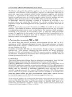
The X-ray diffraction (XRD) measurements shown in Figure 1 indicate that all deposited ITO
films, with thickness 160-200 nm and fabricated from the chemical solutions with different
Sn/In ratio, present a cubic bixebyte structure in a polycrystalline configuration with a (400)
preferential grain orientation.
10 20 30 40 50 60 70
0
2000
4000
6000
8000
(622)
(611)
(440)
(411)
(400)
(222)
T=480 °C
[Sn]/[In]=0 %
[Sn]/[In]=5 %
[Sn]/[In]=11 %
Counts (a. u.)
2 θ (grad)
Fig. 1. XRD spectra of the ITO films fabricated from precursors with different Sn/In ratio
The average size of the grains, 30-50 nm, was determined using the classical Debye-Scherrer
formula from the half-wave of the (400) reflections of the XRD patterns
A surface roughness about 30 nm was determined from images of the films surfaces
obtained with the atomic force microscope (Figure 2).
Fig. 2. AFM images of the In
2
O
3
film (left) and the ITO film with 5% Sn/In (right)
Figures 3 and 4 show the dependence of electric parameters of the spray deposited ITO film
on the ratio Sn/In. The sheet resistance R
s
shown in Figure 3 presents a minimum of 12 Ω/□
the films prepared from the solution with a 5% Sn/In ratio.
Solar Energy
84
Fig. 3. The sheet resistance as a function of the Sn/In ratio in the precursor used for the film
deposition. The thicknesses of the films are also shown
The minimal value of resistivity obtained for the films deposited for the solution with 5%
Sn/In ratio is 2×10
-4
Ω-cm. The variation of mobility and carrier concentration as a function
of the Sn/In ratio are shown in Figure 4.
Fig. 4. Dependence of mobility (μ) and carrier concentration (n) on the Sn/In ratio
Figure 5 shows the optical transmission spectra for the ITO films spray-deposited on a
sapphire substrate as a function of the wavelength for solutions with different Sn/In
contents.
The use sapphire substrates allow for determining the optical energy gap of the ITO films by
extrapolating the linear part of α
2
(hν) curves to α
2
=0, where α is the absorption coefficient.
Efficient Silicon Solar Cells Fabricated with a Low Cost Spray Technique
85
400 600 800 1000 1200
0
20
40
60
80
100
c
b
a
T=480°C
a- Sn/In=0
b- Sn/In=5%
c- Sn/In=11%
Percentage tracmission
Wavelength [nm]
Fig. 5. Optical transmission spectra for the ITO films spray-deposited for different
precursors as a function of the wavelength
The optical gap increases with the carrier concentration, corresponding to the well known
Burstein-Moss shift. For the Ito films fabricated using the solution with a 5% Sn/In ratio this
shift is 0.48 eV, and the optical gap is 4.2 ± 0.1 eV. Such high value for the optical gap offers
transparency in the far ultraviolet range, which is important for the application of these
films in solar cells.
Because of the opposite dependence of the conductivity (σ) and transmission (T) on the
thickness (t) of the ITO, both parameters need to be optimized.
A comparison of the performance for different films is possible using the φ
TC
=T
10
/R
s
=σt
exp(-10αt) figure of merit (Haacke, 1976). Table 1 compares the values of φ
TC
for the spray
deposited ITO films reported in this work with some results obtained by other authors using
different deposition techniques.
Process
R
s
, Ω/□ T (%)
φ
TC,
(Ω
-1
) ×10
-3
Author
spray 26.0 90 13.4 Gouskov, 1983.
spray 9.34 85 21.0 Vasu et al., 1990
spray 10.0 90 34.9 Manifacier, 1981
spray 4.4 85 44.7 Saxena, 1984
sputtering 12.5 95 47.9 Theuwissen, 1984
evaporation 25.0 98 32.6 Nath, 1980
spray 12.0 93.7 43.5 Present work
Table 1. Comparison of the values of φ
TC
for ITO films
3.2 Fluorine-doped tin oxide (FTO) films
The X-ray diffraction (XRD) measurements indicate that all the spray-deposited FTO films
present a tetragonal rutile structure in a polycrystalline configuration with a (200)
Solar Energy
86
preferential grain orientation. The XRD spectra of the FTO films fabricated using precursors
with different F/Sn ratios are shown in Figure 6.
0 204060
0
5
10
15
20
25
30
F/Sn =0
F/Sn=0.35
F/Sn=0.50
F/Sn=0.65
F/Sn=0.85
F/Sn =1
(301)(310)
(211)
(200)
(110)
Counts (x10
3
), a.u.
Angle of diffraction 2
θ
(degree)
Fig. 6. The XRD spectra for the FTO films fabricated using precursors with different F/Sn
ratio
The surface morphology of the films fabricated using precursors with different F/Sn ratio,
and obtained with a scanning electron microscopy (SEM), is shown in Figure 7.
Fig. 7. The surface morphology obtained with a SEM for the films fabricated using
precursors with different F/Sn ratios
The dependence of the average value of the grain size on the F/Sn ratio shows a maximum
(∼ 40 nm) for the films prepared using a precursor with F/Sn=0.5. The roughness variation
Efficient Silicon Solar Cells Fabricated with a Low Cost Spray Technique
87
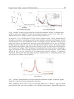
obtained with atomic force microscope for the FTO film fabricated using solutions with
different F/Sn ratios presents a minimum of 8-9 nm at the F/Sn=0.5 ratio.
Figure 8 shows that the electrical characteristics also present some peculiarities for the films
prepared using a precursor with this F/Sn ratio.
Fig. 8. Variation of the sheet resistance (above graph), resistivity (ρ), mobility (μ) and carrier
concentration (n) (below graph) for the FTO films fabricated using precursors with different
F/Sn ratios. The thicknesses of the films are also shown
Solar Energy
88
200 400 600 800 1000
0
20
40
60
80
100
b
c
a
Transmittance [%]
Wavelength [nm]
a- F/Sn-0
b- F/Sn-0.50
c- F/Sn-0.85
0.00.20.40.60.81.0
4.3
4.4
4.5
4.6
4.7
F/Sn ratio in solution
E
g
opt
[eV]
Fig. 9. Optical transmission (above graph) and dependence of the optical gap (below graph)
for the FTO films fabricated using solutions with different F/Sn contents and spray-
deposited on a glass substrate as a function of the wavelength
The optical energy gap (Fig. 9) was determined from the analysis of the absorption spectra
for the films deposited on the sapphire substrate. The Burstein-Moss shift presents a
Efficient Silicon Solar Cells Fabricated with a Low Cost Spray Technique
89
maximum value of 0.6 eV for the films fabricated using the precursor with F/Sn =0.5, which
also corresponds to the highest electron concentration (1.8×10
21
cm
-3
). Figure 10 shows the
Φ=T
10
/R
s
figure of merit for the FTO films reported in this work.
0.0 0.2 0.4 0.6 0.8 1.0
0
20
40
60
80
F/Sn ratio in solution
φ
TC
[10
-3
,
Ω
-1
]
Fig. 10. Variation of the figure of merit Φ=T
10
/R
s
versus the F/Sn ratio used in the solution
for the FTO films reported in this work
The value we obtained for this figure of merit was Φ =75×10
-3
Ω
-1
for the films prepared
using a precursor with F/Sn =0.5; this is more than twice the value (Φ =35×10
-3
Ω
-1
) reported
in the literature (Moholkar et al., 2007) for spray deposited FTO films.
4. Solar cells based on ITO/n-Si heterojunctions
4.1 Physical model of the solar cells
When the ITO (or FTO) film is deposited on the silicon surface, a metal-semiconductor
contact-like is formed due to the metallic electric properties of the degenerated metal oxide.
Ideally, the barrier height (ϕ
b
) formed between the metal and the n-type semiconductor is
determined by the difference between the metal (or in our case the metal oxide) work
function (ϕ
M
) and the electron affinity (χ
s
) in the semiconductor. Actually, the surface states
present in the interface pin the Fermi level, which makes the barrier height less sensitive to
the metal work function (Sze, 2007). The surface has to experiment a reconstruction due to
the discontinuity of the lattice atoms on the surface. Each surface atom present a dangling
bond and shares a dimer bond with its neighbor atom, thus giving place to surface states
inside the Si band gap (Trmop, 1985).
Recently, it has been shown that the barrier height in a metal-silicon junction can take an
almost ideal value if the n-Si surface is passivated with sulfur (Song, 2008). Also the open-
circuit voltage of an Al/ultrathin SiO
2
/n-Si solar cell (Fujiwara, 2003) was improved when
the silicon surface was passivated by a cyanide treatment.
Solar Energy
90
In this chapter we will discuss the properties of the ITO/n-Si solar cells presenting
extremely high values of the potential barrier at the silicon interface obtained by passivating
the surface with a hydrogen-peroxide solution.
If the ITO film is deposited on cleared n-type silicon, the barrier height not exceeds 0.76 eV.
For this value of the barrier height, the ITO/nSi heterojunctions fabricated on silicon
substrates with a resistivity of a few Ω-cm, operate as majority carrier devices, whose
characteristics are well described by the Schottky theory. Usually, such type of devices
present a high value for the dark current originated by the thermo-ionic mechanism, and the
open circuit voltage for these structures designed as solar cells shows a sufficiently low
value. The introduction of a very thin (∼ 2 nm) intermediate SiO
x
layer (Feng, 1979)
decreases the dark current and increases the open-circuit voltage. However, the use of this
approach to improve the characteristics of the surface-barrier solar cells requires a
simultaneous and careful control of the intermediate oxide thickness. Furthermore, the
thermal grown intermediate SiO
x
layer always presents a positive fixed charge located at the
SiO
x
/Si interface, which decreases the barrier height in the case of n-type silicon.
Using known data for the work function of ITO films deposited by spray pyrolysis, whose
average value is reported as 5.0 eV (Nakasa et al., 2005, Fukano, 2005), and the electron
affinity of silicon as 4.05 eV, the ideal barrier height between ITO and n-type silicon is 0.95
eV according to the Mott-Schottky theory. After a treatment of the n-type silicon surface in
the hydrogen-peroxide (H
2
O
2
) solution with a controlled temperature (60
0
C) during 10
minutes, a barrier height of 0.9 eV was obtained with capacitance-voltage measurements.
This value exceeds by 0.14 eV the barrier height obtained after the deposition of the ITO film
on the silicon surface cleaned in HF without the treatment in an H
2
O
2
solution.
It is worth discussing the possible reason for this increment of the barrier height after the
treatment of the silicon surface, as well as the operation of the ITO/n-Si junctions with an
extremely high barrier height. Obviously, a junction with such barrier height fabricated on
the silicon substrates with moderate resistivity could behave as p-n junctions, in which a
surface p-layer is induced by the high surface band bending.
Such situation was obtained (Shewchun, 1980) in solar cells ITO/ultrathin SiO
x
/p-Si
structures. However, in this case the inversion of the conductivity type of the p-Si at the
surface was caused by other factors, such as the low work function of the sputtered ITO film
and the presence of positive charge at the SiO
x
/p-Si interface.
What is the physical reason for the increment of the barrier height in the ITO/n-Si
heterojunctions after the treatment of the silicon substrate in heated 30% H
2
O
2
solutions? It
has been shown (Verhaverbeke, 1997) that the treatment of the silicon in H
2
O
2
leads to the
growth of oxide on the silicon surface. The analysis shows that the main oxidant responsible
for this oxide growth is the peroxide anion, HO
2
¯
. It was also found that the oxide thickness
is limited to a value around 0.8-1.0 nm due to the presence of localized negative charge
(HO
2
¯
) at the silicon surface. From this point of view the HO
2
¯
at the silicon surface can play
a double role. First, these ions can form a chemical composition with the silicon atoms
having dangling bounds in the surface. This can be thought as a passivation of the silicon
surface, which leads to an increment of the potential barrier during the formation of the
ITO/Sl heterostructure. On the other hand, the negative charge of these ions can produce a
band-bending (φ
s
) at the silicon surface due to an outflow of electrons under the influence of
the electrostatic force. Under such conditions, the electron affinity (χ
s
) of the silicon at the
surface will be lower than that at the bulk by Δχ=χ
s
-φ
s
. The presence of a depletion layer at
Efficient Silicon Solar Cells Fabricated with a Low Cost Spray Technique
91
the silicon surface plays an important role for the formation of the potential barrier during
the deposition of the ITO film. The barrier will prevent an electron flow from the silicon to
the ITO film. The surface barrier between the ITO and the silicon will be formed by the flow
of valence electrons from the silicon valence band into the ITO film, creating a hole excess at
the silicon surface. Taking into account the initial band-bending at the silicon surface, the
formation of an inversion layer is possible. As it was already mentioned, the experimentally
determined barrier height at the ITO/Si interface is 0.9 eV. Schematically, the energy
diagram of the ITO/n-Si heterojunction is shown in Figure 11.
Fig. 11. Energy diagram (in kT units) of the heavy doped ITO/n-Si heterojunction
For sake of simplicity, we do not show the very thin (around 1 nm) intermediate SiO
x
layer
present between the ITO film and the silicon, because at this thickness it does not present
any effect on the electro-physical characteristics of the heterojunction. Since the heavily
doped ITO film is a degenerated semiconductor, in which the Fermi level lies above the
minimum of the conduction band, we can consider this ITO film as a “transparent metal.”
The inversion layer at the silicon interface appears when the barrier height φ
b
is higher than
one-half of the Si energy gap. If such inversion p-n junction were connected in a circuit,
which source of holes would be present in order to form an inversion p-layer that
complicates the current flow across the forward-biased structure working as a solar cell? To
answer this question we calculated the number of empty energy states in the conduction
band of a heavy doped ITO, which are available to accept the electrons transferred from the
top of the silicon valence band located at a distance
Δ
below the Fermi level (Malik et al.,
2006). The probability that an energy state E below the Fermi level E
FM
in the degenerated
ITO is empty was calculated using the Fermi-Dirac distribution. Using a barrier height
φ
n
=0.9 eV, Δ=0.3 eV, and three different values for (E
FM
-E
CM
), which is the distance between
the Fermi level an the conducting band of the ITO. This characterizes the degree of
degeneration of the ITO film. The calculated number of empty states available to accept the
E
FM
/kT
E
CM
/kT=0
Δ
E/kT
E
CS
/kT
E
FS
/kT
ξ
(ITO)
φ
b
/kT
eφ
p
/kT
x = 0
x
E
opt
g
/kT
E
VS
/kT
Solar Energy
92
electrons from the silicon valence band forming the additional amount of the holes is shown
in Figure 12 as triangles. For comparison the number of empty states in the case of a
gold/silicon contact with the same barrier height is also shown. For such calculations, the
difference between the effective mass of electrons in the ITO and that in gold has been taken
into account.
Fig. 12. Calculated number of empty states available to accept the electrons from the silicon
valence band (Malik et al., 2006)
From the discussion presented above, and the amount of the calculated number of empty
states in the ITO, leads to the important conclusion that a heavy doped ITO layer serves as
an efficient source of holes necessary to form the inversion p-layer in the ITO/n-Si
structures.
4.2 Evidence of the inversion in the type conductivity in the ITO/n-Si heterostructures
Based on the barrier height (0.9 eV) obtained from the measured C-V characteristics for the
ITO/n-Si heterostructures on 10 Ω-cm monocrystalline silicon, one can discuss about the
physical nature of such heterojunctions. Because the barrier height exceeds one half of the
silicon band gap, the formation of an inversion p-layer at the silicon surface is obvious from
the band diagram. To avoid any speculations on this issue and in order to present a clear
evidence for the existence of a minority (hole) carrier transport in these heterojunctions, a
bipolar transistor structure was fabricated on a 10 Ω-cm monocrystalline silicon substrate, in
which the emitter and the collector areas, on opposite sides of the silicon substrate, were
fabricated based on the ITO/n-Si junctions. The ITO film was deposited using the spray
deposition technique described in section 2.1 followed by a photolithographic formation of
the emitter and the collector areas. The treatment in the H
2
O
2
solution described above was
applied to the silicon substrate. An ohmic n
+
-contact (the base) was formed using local
diffusion of phosphorous in the silicon substrate. The dependence of the collector current
versus the collector-base voltage, using the emitter current as a parameter, are shown in
Efficient Silicon Solar Cells Fabricated with a Low Cost Spray Technique
93
Figure 13, together with the emitter injection efficiency of the ITO/n-Si/ITO transistor
(Malik et al., 2004).
Fig. 13. Dependence of the collector current on the collector-base voltage (the emitter current
is used as a parameter). The emitter injection efficiency of the ITO/n-Si/ITO transistor
fabricated on a 10 Ω-cm silicon substrate is also shown. (Malik et al., 2004)
Hence, even in non-optimized transistors (wide base), an efficient hole injection of around
0.2 was observed. This is an obvious evidence of the existence of an inversion layer in the
ITO/n-Si heterostructures with a barrier height of 0.9 eV. We can also present two indirect
evidences of the p-n nature of the ITO/n-Si heterojunctions. The first one is based on the
observation of an efficient radiation emission from the ITO/n-Si structures under a forward
bias (Malik et al., 2004). In metal-semiconductor contacts operated as majority carriers’
devices (described by the Schottky theory), the injection ratio does not exceed 10
-4
. Thus, an
efficient electroluminescence, in contrast to our devices, is not possible to observe. The next
evidence is based on the observed modulation of the conductivity in the forward-biased
ITO/n-Si diodes fabricated on high resistivity silicon, which operate as p-i-n diodes. So, the
0.9 eV barrier height belongs to an inversion ITO/n-Si heterojunction. This gives us the
Solar Energy
94
possibility to analyze theoretically such structures based on the well-known theory of p-n
junctions.
4.3 Limit of applicability of the p-n model for the ITO/n-Si solar cells
Once we know the physical nature of the ITO/n-Si heterojunctions with extremely high
potential barrier, it is possible to apply correctly the theory for their modelling, which is
known as the theory of p-n based solar cells. The problem now is to find the range of
resistivity of the silicon substrate on which the p-n theory can be applied to the ITO/n-Si
heterojunction with extremely high potential barrier. Based on results published recently
(Malik et al., 2008), the condition for strong inversion in the ITO/n-Si heterojunction
requires that
(
)
iFs
EE
−
≥ 2
ϕ
, (1)
where
)/ln(
idiF
nNkTEE
=
−
, (2)
s
ϕ
is the surface potential at the Si/SiO
x
interface, k is the Boltzmann constant, T is the
temperature, n
i
is the intrinsic carrier concentration, and N
d
is the donor concentration in the
n-Si substrate. On the other hand,
)(
FCbs
EE −−=
ϕϕ
, (3)
)/ln(
dCFC
NNkTEE
=
−
, (4)
where
b
ϕ
is the potential barrier for carriers from the ITO side of the structure, and N
C
is the
effective density of states in the conduction band.
Moreover, the surface hole concentration is
)/exp()/()0(
2
kTNnxp
sds
i
ϕ
==
(5)
Combining equations (2)-(5), it is possible to obtain the surface concentration of the minority
carriers at the Si/SiO
x
interface under strong inversion of the conductivity type:
(
)
)./exp()/(0
2
kTNnxp
bCs
i
ϕ
==
(6)
This concentration depends only on the barrier height and not on N
d
. Figure 14 shows the
two possible models in the space p
s
(x=0)/N
d
vs. N
d
in the substrate for different barrier
heights.
The two shaded areas are related to the two possible models: a Schottky model for
p
s
(x=0)/N
d
<0.01 and an induced p-n junction, in which p
s
(x=0)/N
d
>10. For instance, at a
barrier height of 0.7 V, the green line takes two intercepts: one with the border of the area
that is related to the Schottky barrier model, and the other one with the border of the area
that is valid for the p-n inversion model. Thus, for N
d
>3x10
14
cm
-3
the structures behave as
Schottky-barrier structures, whereas the structures with N
d
<4x10
13
cm
-3
, behave as p-n
Efficient Silicon Solar Cells Fabricated with a Low Cost Spray Technique
95
10
13
10
14
10
15
10
16
10
-7
1
x10
-5
10
-3
10
-1
10
1
10
3
p
s
/N
d
N
d
[cm
-3
]
ϕ
b
=0.6 V
ϕ
b
=0.7 V
ϕ
b
=0.8 V
ϕ
b
=0.9 V
p
s
(x=0)/N
d
<0.1
p
s
(x=0)/N
d
>10
Fig. 14. Schematically representation of two possible models of the ITO/n-Si heterojunction
in coordinates of p
s
(x=0)/N
d
vs. concentration N
d
in the silicon substrate. The different
barrier height serves as a parameter (Malik et al., 2008)
junctions. With the potential barrier height of 0.9 eV achieved in this work, the structures
may be considered as a symmetrical p-n (
ds
Np
=
) for N
d
=8x10
15
cm
-3
(0.3 Ω-cm resistivity
of the substrate), or as an asymmetrical p
+
-n junctions (
ds
Np 10≥
) for N
d
=8x10
14
cm
-3
(5 Ω-
cm resistivity of the substrate). Due to the substrate resistivity used in this work, 10 Ω-cm
(N
d
=5x10
14
cm
-3
), our solar cells with a barrier height of 0.9 eV present an asymmetrical p
+
-n
junctions, and the theoretical analysis of such structures will be conducted based on the
theory of p+-n junctions.
We underline again that the intermediate SiO
x
layer formed after the treatment of the silicon
substrate in the H
2
O
2
solution is sufficiently “transparent” for the carriers; then the
tunneling current through this layer provides an ohmic contact between the ITO film and
the surface-induced p
+
-Si layer.
Thus, we can apply the diffusion theory of the p-n junction based solar cells for modelling
the ITO/n-Si solar cells with a barrier height of 0.9 eV (the barrier height does not depend
on the substrate carrier concentration) for a silicon substrate resistivity higher than 0.5 Ω-cm
(or a carrier concentration lower than 8×10
15
cm
-3
).
4.4 ITO/n-Si solar cells: design, fabrication and characterization
The solar cells were fabricated using (100) n-type (phosphorous doped) single-crystalline
silicon wafers with a 10 Ω-cm resistivity. Both sides of the wafer were polished. Standard
wafer cleaning procedure was used. To form the barrier, an 80 nm-thick ITO film with a
sheet resistance of 30 Ω/□ was deposited by spray pyrolysis on the silicon substrate treated
Solar Energy
96
in the H
2
O
2
solution. This ITO thickness was chosen in order to obtain an effective
antireflection action of the film. Metal, as an ohmic contact in the back side of the wafer, was
deposited on an n
+
-layer previously created by diffusion. The device area for measurements
was 1-4 cm
2
. Approximately 1 μm-thick Cr/Cu/Cr film was evaporated through a metal
mask to create a grid pattern (approximately 10 grid-lines/cm). After fabrication, the
capacity-voltage characterization was conducted to control the value of the potential barrier.
Then the following parameters were measured under AMO and AM1.5 illumination: open
circuit voltage V
oc
, short circuit current I
sc
, fill factor FF, and efficiency. No attempt was
made to optimize the efficiency of the cells by improving the collection grid. The series
resistance (R
s
) of the cell was measured using the R
s
=(V-V
oc
)/I
sc
relationship (Rajkanan,
Shewchun, 1979), where V is the voltage from the dark I-U characteristics evaluated at I=I
sc
.
It was shown above that the ITO/n-Si heterostructures with a potential barrier height at the
silicon surface of 0.9 eV behave as pseudo classical diffusion p-n junctions. Thus, it is
expected that the diffusion of holes in the silicon bulk dominates the carrier transport
instead of the dominance of the thermo-ionic emission in the Schottky and the metal/tunnel
oxide/semiconductor structures. A straightforward measurement of the dependence of the
dark current on temperature is, in principle, sufficient to identify a bipolar device in which
the thermo-ionic current is negligible in comparison to the minority-carrier diffusion current
J
d
(in units of current density). A simple Shockley’s analysis of the p-n diode including the
temperature dependence of the silicon parameters (diffusion length, diffusion coefficient,
minority carrier life-time, and the intrinsic concentration) (Tarr, Pulfrey, 1979) shows that
0
[exp ( / ) 1]
dd
JJ qVkT
=
−
(7)
and
00
exp ( / )
dg
J
TEkT
γ
∝−
, (8)
where γ = 2.4 and E
g0
= 1.20 eV.
From Eq.(8) it can be seen that the plot log(J
0d
/T
γ
) vs. 1/T should produce a straight line,
and that the slope of this line should be the energy E
g0
. In the case of MS and MIS devices
this slop must be equal to the value of the barrier ϕ
b
.
Usually, the series resistance of the device affects the I-V characteristics at high forward
current densities. To prevent this effect, we must measure the J
sc
vs V
oc
dependences
(Rajkanan, Shewchun, 1979). The photogenerated current is equal to the saturation
photocurrent. For minority-carrier MIS diode with a thin insulating layer (Tarr, Pulfrey,
1979)
)()(
ocdocrgsc
VJVJJ
+
=
. (9)
For an increasing bias, J
d
increases faster than the recombination current density J
rg
; in the
high illumination limit we should have
),/exp(
0
nkTqVJJ
ocdsc
=
(10)
which gives an n factor approximately equal to 1.
Figure 15 shows the measured dependence of J
sc
on V
oc
at room temperature. The value of
J
0d
in (10) was determined by measuring J
sc
and V
oc
at different temperatures, and under
Efficient Silicon Solar Cells Fabricated with a Low Cost Spray Technique
97
illumination with a tungsten lamp. An optical filter was used to prevent the heating of the
cell by the infra-red radiation. For each J
sc
- V
oc
pair lying in the range where n ≈ 1, J
0d
=J
02
was calculated from (10). After making the correction for the
γ
T
factor appearing in Eq.(8),
the J
0d
values were plotted as a function of the reciprocal temperature, as shown in the insert
of Figure 15.
0 5 10 15 20 25
10
-6
1x10
-5
1x10
-4
10
-3
10
-2
10
-1
3.5 4.0 4.5 5.0
10
-20
10
-17
1x10
-14
1x10
-11
±
±
±±
E
0d
= 1.21± 0.02 eV
J
02
[A/cm
2
]
1000/T [K
-1
]
160 200 240 280
0,90
0,92
0,94
0,96
Barrier Height [eV]
Temperature [K]
n = 1.02
(J
02
)
n = 2.26
(J
01
)
J
SC
[A/cm
2
]
qV
OC
/kT
Fig. 15. Measured dependence of J
sc
on V
oc
at room temperature, and calculated dependence
of the current density J
02
=J
0d
at high illumination level corrected for the
γ
T
factor, as function
of reciprocal temperature for ITO/n-Si solar cells with the barrier height of 0.9 eV. The
dependence of the barrier height on temperature is also shown in the insert
The slope of the J
02
vs. 1/T line was found to correspond to an energy E
g0
from Eq.(8). It can
be concluded that for high current densities the current in the cell is carried almost
exclusively by holes injected from the ITO contact that later diffuse into the base of the cell.
The output characteristics of the ITO/n-Si solar cell measured under AM0 and AM1.5
illumination conditions, as well as the calculated dependence of output power of the cell
versus the photocurrent, are shown in Figure 16.
Solar Energy
98
Fig. 16. I-V characteristics (above graph) of the ITO/n-Si solar cell measured under AM0
and AM1.5 illumination conditions, and the calculated dependence of the output power of
the cell (below graph) versus the photocurrent
The fill factor (FF) and the efficiency calculated from these characteristics are 0.68 and 10.8%
for AM0 illumination conditions; and 0.68 and 12.1% for AM1.5 illumination conditions. The
fill factor and efficiency obtained are not optimized because of the cell design and the used
silicon substrate with relatively high resistivity. Below, a theoretical analysis followed for
increasing the output parameters of the cells using silicon substrates with lower resistivity is
presented.
Efficient Silicon Solar Cells Fabricated with a Low Cost Spray Technique
99
4.5 Optimization of the output characteristics of the cells: theoretical analysis
Recently, a detailed theoretical modelling of the ITO/n-Si solar cells has been reported
(Malik et al, 2008). Based on these published results, here we show the most important
conclusions; further details can be consulted in that work.
For all the calculations, the thickness of the silicon substrate, sheet resistance and thickness
of the ITO film were taken as d=500 μm, 30 Ω/, and t=80 nm, respectively. We considered
the case when the diffusion length of minority carriers is shorter than the thickness of the
silicon substrate, and assumed that the carrier recombination rate at the back contact of the
silicon substrate is infinite. The total series resistance of the cell with an area of 1 cm
2
used
for these calculations was taken as 1.8 Ω.
In order to calculate the theoretical parameters of the solar cells we assumed also that the
equation for the I-V characteristic for an illuminated cell (Sze & Ng, 2007) is
()
00
ln 1
sc s
s
sh
JJ VJR
q
VJR
JJR kT
γ
⎛⎞
+−
−+=−
⎜⎟
⎝⎠
, (11)
where J is the current density, J
0
the saturation dark current density, J
sc
is the short-circuit
current density, V is the output voltage, R
s
and R
sh
are the series and shunt resistances, and
γ
is the “ideality” factor of the solar cell. According to our experimental results,
γ
was taken as
1 for the calculations.
In order to calculate the photocurrent density we integrated the next equation based on the
spectral distribution of the incident solar radiation, and the parameters of silicon (absorption
coefficient α(λ), diffusion length for minority carriers L
p
, and thickness of the silicon
substrate d):
2
22
1
(1 ) (1 ) (1 )
1
d
p
p
W W
sc p
p
p
d
cosh e
L
L
J
qRF e L RFed
L
d
sinh
L
α
λ
α α
λλ λλ
λ
α
α
λ
α
−
− −
⎧⎫
⎛⎞
⎛⎞
⎪⎪−
⎜⎟
⎜⎟
⎜⎟
⎛⎞
⎪⎪
⎜⎟
⎝⎠
=− ×− +− −
⎜⎟
⎨⎬
⎜⎟
⎜⎟
−
⎛⎞
⎪⎪
⎝⎠
⎜⎟
⎜⎟
⎪⎪
⎜⎟
⎜⎟
⎝⎠
⎝⎠
⎩⎭
∫
(12)
where q is the electron charge, W is the depletion width in the silicon substrate, and R(λ) is
the spectral reflectance from the ITO/Si interface calculated from the optical constants of
silicon and ITO (Malik et al, 2008).
The spectral distribution F
λ
of the solar radiation, which are related to the AM0 (136
mW/cm
2
) and AM1.5 (100 mW/cm
2
) conditions, have been used in the calculations
according to the 2000 ASTME-490-00 and ASTM G-173-03 standards, respectively.
The values of the open-circuit voltage under AM0 and AM1 conditions were calculated
according to the equation
⎟
⎟
⎠
⎞
⎜
⎜
⎝
⎛
+= 1ln
0
J
J
q
kT
V
sc
oc
γ
, (13)
where the saturation dark current density J
0
is calculated from the equation
Solar Energy
100
2
0
i
p
dp p
D
d
Jqn coth
NL L
=
(14)
Here, n
i
and N
d
are the intrinsic and donor concentrations in the silicon substrate,
respectively, and D
p
is the diffusion coefficient for holes.
Figure 17 shows the experimental (dots) and calculated (lines) I-V characteristics of the solar
cell (using equation (11)) with an area of 1 cm
2
fabricated on 10 Ω-cm silicon under both
AM0 and AM1.5 illumination conditions. Initially, these characteristics were calculated
using J
sc
= 40 mA/cm
2
, R
s
= 1.8 Ω, and R
sh
= ∞. Then, in order to improve the fitting with the
experimental results, the calculated characteristics were corrected using R
sh
= 300 Ω. One can
see an excellent coincidence between the experimental and calculated characteristics, as well
as for the parameters of the cell (fill factor F.F. and conversion efficiency
η
).
Fig. 17. Experimental (dots) and calculated (solid lines, using equation (11)) I-V
characteristics of the solar cell with an area of 1 cm
2
, and fabricated on a 10 Ω-cm silicon
substrate, under both AM0 and AM1.5 illumination conditions
Figure 18 (above graph) shows the dependence of the short-circuit current density J
sc
on the
diffusion length in the silicon substrate, under AM0 and AM1.5 illumination conditions.
The values of the open-circuit voltage under the same conditions were calculated according
to equations. (13) and (14). From equation (14), the value of J
0
decreases with the resistivity
ρ
of the silicon substrate. The calculated dependence for the open-circuit voltage (V
OC
) on the
resistivity of the Si substrate is also shown in Figure 18 (below graph).
The calculations show that the conversion efficiency of the ITO-SiO
x
-nSi solar cells can be
improved by using silicon with a lower resistivity. Under the AM1.5 conditions, the
calculated dependences of the open circuit voltage, fill factor, and efficiency on the
Efficient Silicon Solar Cells Fabricated with a Low Cost Spray Technique
101
resistivity of the silicon substrate, are shown in Figure 19. The surface recombination
velocity (S
p
) was taken into account for these calculations. The value of S
p
for the ITO/n-Si
heterostructures under investigation, and determined from the analysis of the transistor
structures, was 500 cm/s approximately.
0 100 200 300 400 500
15
20
25
30
35
40
AM1.5
AM0
J
sc
[ mA/cm
2
]
Diffusion length L
p
[
μ
m]
0 5 10 15 20
0.48
0.50
0.52
0.54
0.56
0.58
0.60
0.62
d
c
b
a
AM0 d=500
μ
m
Voc [ Volts ]
Resistivity [ Ohms-cm ]
a Lp=100
μ
m
b
Lp=200
μ
m
c
Lp=300
μ
m
d
Lp=400
μ
m
Fig. 18. Calculated dependence of J
sc
and V
OC
for the ITO/n-Si solar cells
Solar cells fabricated on silicon substrates with a resistivity of 1Ω-cm and a hole diffusion
length of L
p
= 200 μm may present an efficiency of 14 %. For an experimentally found
potential barrier of 0.9 eV it is not possible to achieve a further reduction of the silicon
resistivity for structures with a p-n inversion layer or minority carrier devices. Such
structures are majority carrier devices, and their properties are described by the theory of
Schottky barriers. In such cases, a lower efficiency is expected due to a higher saturation
current. Solar cells using FTO films present similar characteristics.
Solar Energy
102
Fig. 19. Calculated dependences of the series resistance, fill factor, and efficiency of the cells,
on the resistivity of the silicon substrate.
5. Conclusions
ITO-nSi solar cells have been produced using a spraying technique. Transparent and
conductive tin-doped indium oxide films, as well as fluorine-doped tin oxide films,
presenting excellent structural, optical and electrical parameters, were fabricated using a
very simple, low cost, and no-time consuming method. The cells obtained in such a way can
be considered as structures presenting an inversion p-n junction. Under the AM0 and AM1.5
solar illumination conditions, the efficiency is 10.8% and 12.2%, respectively. The theoretical
modelling based on p-n solar cells show an excellent coincidence between the theoretical
and the experimental results. It is also shown that using 1 Ω-cm silicon substrates is a
promising alternative for obtaining solar cells with 14% efficiency under AM1.5 illumination
conditions. The use of substrates with a lower resistivity leads to a reduction of the
conversion efficiency due to the formation of Schottky barriers, which gives place to a
higher saturation dark current than that presented by p-n structures. The fabrication of
reported solar cells is more controllable than that needed for obtaining metal-insulator-
silicon solar cells because of the necessity of controlling a very thin (nearly 2 nm)
intermediate oxide layer on the silicon substrate. Moreover, a detailed theoretical analysis
(Shewchun et al., 1980) shows a higher efficiency for p-n inversion solar cells in comparison
with those based on majority-carrier MIS structures.
6. References
Ashok, S.; Sharma, P. & Fonash, S. (1980). Spray-deposited ITO-silicon SIS heterojunction
solar cells. IEEE Trans. Electron. Dev., Vol.ED-27, N.4, 725-730, ISSN 0018-9383
Efficient Silicon Solar Cells Fabricated with a Low Cost Spray Technique
103
Dawar, A. & Joshi J. (1984). Semiconducting transparent thin films: their properties and
applications. J. Mater. Sci., Vol.19, 1-23, ISSN 0022-2461
DuBow, J.; Burk, D. & Sites, J. (1976). Efficient photovoltaic heterojunctions of indium tin
oxides on silicon. Appl. Phys. Lett., Vol.29, N.8, 494-496, ISSN 0003-6951
Feng, T.; Ghosh, A. & Fishman, G. (1979). Efficient electron-beam-deposited ITO/n-Si solar
cells, J. Appl. Phys., Vol.50, N.7, 4972-4974, ISSN 0022-3727
Fukano, T.; Motohiro, T. & Ida, T. (2005). Ionization potential of transparent conductive
indium oxide films covered with a single layer of fluorine-doped tin oxide
nanoparticles grown by spray pyrolysis deposition, J. Appl. Phys., Vol.97, N.8,
Nanoscale science and design, ISSN 0022-3727
Fujiwara, N.; Fujinaga, T.; Niinobe, D.; Maida, O.; Takahashi, M. & Kobayashi, H. (2003).
Passivation of defect states in Si and Si/SiO
2
interface states by cyanide treatment:
improvement of characteristics of pin-junction amorphous Si and crystalline Si-
based metal-oxide-semiconductor junction solar cells. Acta Phys. Slovaca, Vol.53,
N.3, 195-205, ISSN 0323-0465
Granqvist, C. (1993). Transparent Conductive Electrodes for Electrochromic Devices: A
Review. Appl. Phys., Vol.A57, 19-24, ISSN 0947-8396
Gouskov, L.; Saurel, J.; Gril, C.; Boustani, M. & Oemry, A. (1983). Sprayed indium tin oxide
layers: Optical parameters in the near-IR and evaluation of performance as a
transparent antireflecting and conducting coating on GaSb or Ga
1-x
Al
x
Sb for IR
photodetection. Thin Solid Films, Vol.99, N.4, 365-369, ISSN 0040-6090
Haacke, J. (1976). New figure of merit for transparent conductors. J. Appl. Phys., Vol.47, 4086-
4089, ISSN 0022-3727
Hamberg, J. & Granqvist, C. (1986). Evaporated Sn-doped In2O3 films: basic optical
properties and applications to energy-efficient windows. J. Appl. Phys., V.60, n.11,
R13, ISSN 0022-3727
Hartnagel, H.; Dawar, A.; Jain, A. & Jagadish, C. (1995). Semiconducting Transparent Thin
Films, IOP Publishing Ltd., ISBN 0 7503 03220, Bristol UK
Malik, A.; Baranyuk, V. & Manasson, V. (1979). Solar cells based on the SnO
2
–SiO
2
-Si
heterojunction. Appl. Sol. Energy, N. 2, 83-84, ISSN 0003-701X
Malik, A.; Baranyuk, V. & Manasson, V. (1980). Improved model of solar cells based on the
In
2
O
3
/ SnO
2
-
SiO
x
-nSi structure. Appl. Sol. Energy, N.1, 1-2, ISSN 0003-701X
Malik, O.; Grimalsky, V.; Torres-J., A. & De la Hidalga-W, J. Room Temperature
Electroluminescence from Metal Oxide-Silicon. Proceedings of the 16
th
International
Conference on Microelectronics (ICM 2004), pp. 471-474, ISBN 0-7803-8656-6, Tunis,
December 06-08, 2004, IEEE, Tunisia
Malik, O.; Grimalsky, V. & De la Hidalga-W, J. (2006). Spray deposited heavy doped indium
oxide films as an efficient hole supplier in silicon light-emitting diodes. J. Non-
Cryst. Sol., Vol.352, 1461-1465, ISSN 0022-3093
Malik, O.; De la Hidalga-W, J.; Zúñiga-I, C. & Ruiz-T, G. (2008). Efficient ITO-Si solar cells
and power modules fabricated with a low temperature technology: results and
perspectives. J. Non-Cryst. Sol., Vol.354, 2472-2477, ISSN 0022-3093
Manifacier, J. & Szepessy, L. (1977). Efficient sprayed In
2
O
3
:Sn n-type silicon heterojunction
solar cell. Appl. Phys. Lett., Vol.31, N.7, 459-462, ISSN 0003-6951
Manifacier, J.; Fillard, J. & Bind J. (1981). Deposition of In
2
O
3
-SnO
2
layers on glass substrates
using a spraying method. Thin Solid Films, Vol. 77, N.1-3, 67-80, ISSN 0040-6090
Solar Energy
104
Moholkar, A.; Pawar, S.; Rajpure, K.; & Bhosale, C. (2007). Effect of solvent ratio on the
properties of highly oriented sprayed fluorine-doped tin oxide thin films. Mater.
Lett., Vol.61, N.14-15, 3030-3036, ISSN 0167-577X
Nagatomo, T.; Endo, M. & Omoto, O. (1979). Fabrication and characterization of SnO2/n-Si
solar cells, Jpn. J. Appl. Phys., Vol.18, 1103-1109, ISSN 0021-4922
Nagatomo, T.; Inagaki, Y.; Amano, Y. & Omoto, O. (1982). A comparison of spray deposited
ITO/n-Si and SnO2/n-Si solar cells, Jpn. J. Appl. Phys., Vol.21, N. 21-2, 121-124,
ISSN 0021-4922
Nakasa, A.; Adachi, M.; Suzuki, E.; Usami, H. & Fujimatsu, H. (2005). Increase in
conductivity and work function of pyrosol indium tin oxide by infrared irradiation,
Thin Solid Films, Vol.84, N.1-2, 272-277, ISSN 0040-6090
Nath, P. & Bunshah, R. (1980). Preparation of In
2
O
3
and tin-doped In
2
O
3
films by novel
activated reactive evaporation technique. Thin Solid Films, Vol.69, N.1, 63-68, ISSN
0040-6090
Rajkanan, K. & Shewchun, J.(1979) A better approach to the evaluation of the series
resistance of solar cells, Sol. St. Electron., Vol.22, N.2-E, 193-197, ISSN 0038-1101
Saxena, A.; Singh, S.; Thangaraj, R. & Agnihotri O. (1984). Thickness dependence of the
electrical and structural properties of In
2
O
3
:Sn films, Thin Solid Films, Vol.117, N.2,
95-100, ISSN 0040-6090
Shewchun, J.; Burc, D. & Spitzer, M. (1980). MIS and SIS solar cells, IEEE Trans. Electron.
Dev., Vol.ED-27, N.4, 705-716, ISSN 0018-9383
Song, G.; Ali, M. & Tao, M. (2008). A high Schottky barrier between Ni and S-passivated n-
type Si (100) surface. Sol. St. Electron., Vol.52, 1778-1781, ISSN 0038-1101
Sze, S. & Ng, K. (2007). Physics of semiconductor devices, 3
rd
ed., John Wiley and Sons, ISBN
9780471143239, N.Y.
Tarr, N. & Pulfrey, D. (1979). New experimental evidence for minority-carrier MIS diodes.
Appl. Phys. Lett., V.34, N.4, 15 February 1979, 295-297, ISSN 0003-6951
Theuwissen, A. & Declerck, G. (1984). Optical and electrical properties of reactively d. c.
magnetron-sputtered In
2
O
3
:Sn films. Thin Solid Films, Vol.121, N.2, 109-119, ISSN
0040-6090
Trmop, R.; Hamers, R. & Demuth, J. (2005). Si (100) dimmer structure observed with
scanning tunneling microscopy, Phys. Rev. Lett., Vol.55, N.12, 1303- 1308, ISSN
0031-9007
Vasu, V. & Snbrahmanyam, A. (1990). Reaction kinetics of the formation of indium tin oxide
films grown by spray pyrolysis. Thin Solid Films, Vol.193-194, n.2, 696-703, ISSN
0040-6090
Verhaverbeke, S.; Parker, J. & McConnell, C. (1997). The role of HO
2
¯
: in SC-1 cleaning
solutions. In: Mat. Res. Soc. Symp. Proc., Vol. 477: Science and Technology of
Semiconductor Surface Preparation, 47-56, MRS, ISBN 1-55899-381-9, N.Y.
6
Efficiency of Thin-Film CdS/CdTe Solar Cells
Leonid Kosyachenko
Chernivtsi National University
Ukraine
1. Introduction
Over the last two decades, polycrystalline thin-film CdS/CdTe solar cells fabricated on glass
substrates have been considered as one of the most promising candidates for large-scale
applications in the field of photovoltaic energy conversion (Surek, 2005; Goetzberger et al.,
2003; Romeo et al., 2004). CdTe-based modules have already made the transition from pilot
scale development to large manufacturing facilities. This success is attributable to the
unique physical properties of CdTe which make it ideal for converting solar energy into
useful electricity at an efficiency level comparable to traditional Si technologies, but with the
use of only about 1% of the semiconductor material required by Si solar cells.
To date, the record efficiencies of laboratory samples of CdS/CdTe solar cells and large-area
modules are ~ 16.5 % and less than 10 %, respectively (Britt & Ferekides, 1993; Hanafusa et
al., 1997; Meyers & Albright, 2000; Wu et al., 2001; Hanafusa et al., 2001; Bonnet, 2003). Thus,
even the record efficiency of such type solar cells is considerable lower than the theoretical
limit of 28-30% (Sze, 1981). Next challenge is to improve the performance of the modules
through new advances in fundamental material science and engineering, and device
processing. Further studies are required to reveal the physical processes determining the
photoelectric characteristics and the factors limiting the efficiency of the devices.
In this chapter, we present the results of studying the losses accompanying the photoelectric
conversion in the thin-film CdS/CdTe heterostructures and hence reducing the efficiency of
modules on glass substrate coated with a semitransparent ITO or SnO
2
conducting layer. We
discuss the main parameters of the material used and the barrier structure determining the
photoelectric conversion efficiency in CdS/CdTe solar cell: (i) the width of the space-charge
region, (ii) the lifetime of minority carriers, (iii) their diffusion length and drift length,
(iv) the surface recombination velocity, and (v) the thickness of the CdTe absorber layer.
Among other factors, one of the important characteristics determining the efficiency of a
solar cell is the spectral distribution of the quantum efficiency which accounts for the
formation of the drift and diffusion components of the photocurrent and ultimately the
short-circuit current density. In the paper particular attention is given to this aspect of solar
cell. We demonstrate the possibility to describe quantitatively the quantum efficiency
spectra of the thin-film CdS/CdTe solar cells taking into account the recombination losses at
the CdS-CdTe interface and the back surface of the CdTe absorber layer.
Charge collection efficiency in thin-film CdS/CdTe solar cells are also discussed taking into
consideration losses caused by a finite thickness of the p-CdTe layer, recombination losses at
the front and back surfaces as well as in the space-charge region. The dependences of the
Solar Energy
106
drift and diffusion components of short-circuit current on the uncompensated acceptor
concentration, charge carrier lifetime, recombination velocities at the interfaces are
evaluated and discussed.
The mechanism of the charge transport in the CdS/CdTe heterostructure determining the
other photoelectric parameters of the solar cell, namely, the open-circuit voltage and fill
factor is also considered. It is shown that the above-barrier (diffusion) current of minority
carriers is important only at high bias voltage, and the dominant charge transport
mechanism is the generation-recombination occurring in the depletion layer. The observed
I–V characteristics in the dark and the light are described mathematically in the context of
the Sah-Noyce-Shockley theory.
2. Spectral distribution of quantum efficiency of CdS/CdTe heterostructure
In this section we will describe mathematically the spectral distribution of quantum
efficiency of the thin-film CdS/CdTe solar cells taking into account the main parameters of
the material used and the barrier structure, recombination in the space-charge region, at the
CdS-CdTe interface and the back surface of the CdTe absorber layer.
Quantum efficiency η
ext
is the ratio of the number of charge carriers collected by the solar
cell to the number of photons of a given energy (wavelength
λ
) shining on the solar cell.
Quantum efficiency relates to the response (A/W) of a solar cell to the various wavelengths
in the spectrum. In the case of monochromatic radiation (narrow spectral range) η
ext
(λ)
relates to the radiation power P
opt
and the photocurrent I
ph
by formula
ph
ext
opt
/
()
/
Iq
Ph
ηλ
ν
=
, (1)
where q is the electronic charge, h
ν
is the photon energy.
2.1 Experimental
Fig. 1(a) shows the quantum efficiency spectra of the CdS/CdTe solar cell taken at different
temperatures. The substrates used for the development of thin film layers were glass plates
coated with a semitransparent ITO (SnO
2
+ In
2
O
3
) layer. The window layer CdS (∼ 0.1 µm)
was developed by chemical bath deposition (CBD); the absorber layer CdTe (1-3 µm) was
deposited on top of CdS by close-space sublimation (CSS) (Mathew et al., 2007).
Non-rectifying ohmic contact to the CdTe layer was fabricated by sputtering Ni in vacuum
after bombarding the CdTe surface by Ar ions with energy ~ 500 eV. The electrical
characteristics of two neighboring Ni contacts on the CdTe surface were linear over the
entire range of measured currents.
The spectral characteristics of the samples in the 300-900 nm range were recorded with a
photoresponse spectral system equipped with a quartz halogen lamp. The spectral
distribution of the photon flux at the outlet slit of the system was determined using a
calibrated Si photodiode.
As can be seen from Fig. 1(a), compared with the literature data, the measured curves seem
to reflect the most common features of the corresponding spectral curves for these devices
(Sites et al., 2001; McCandless et al., 2003; Ferekides et al., 2004).
In the long-wavelength region, the spectra are restricted to the value
λ
g
corresponding to the
band gap of CdTe which is equal to 1.46 eV at 300 K (
λ
g
= hc/E
g
= 845 nm). In the short-
Efficiency of Thin-Film CdS/CdTe Solar Cells
107
300 500 700 90
0
0
0.1
0.2
0.3
0.4
λ
(
nm
)
η
(λ)
356 K
246
K
293 K
315 K
336 K
271
K
0
0.2
0.4
0.6
0.8
1.0
500 700 900
λ
(nm)
T
ITO
,
T
CdS
300
T
CdS
T
ITO
Fig. 1. (a) Spectral distribution of the quantum efficiency of CdS/CdTe device measured at
different temperatures. (b) The transmission curves of the ITO coated glass (T
ITO
) and the
CdS layer (T
CdS
) as a functions of the wavelength
λ
.
wavelength side, the quantum efficiency decays due to the lower transmission through the
thin film layers: CdS in the range
λ
< 500-520 nm and ITO at
λ
< 350 nm (Fig. 1(b)).
The external quantum efficiency
η
ext
is related with the quantum efficiency of photoelectric
conversion in the CdTe absorber layer, the transmission of the glass plate coated by ITO,
T
ITO
, and the transmission of the CdS layer, T
CdS
, by the expression:
ext ITO CdS int
TT
η
η
=
(2)
where
η
int
is the ratio of photogenerated carriers collected to the photon flux that arrives at
the CdTe absorber layer.
In order to describe the external quantum efficiency spectrum
η
ext
we used the measured
spectral dependences T
ITO
(
λ
) and T
CdS
(
λ
) shown in Fig. 1(b). The quantum efficiency
η
int
will
be determined in the following by considering the photoelectric processes in the diode
structure.
2.2 Width of the space-charge region and energy diagram of thin-film CdS/CdTe
heterostructure
One of the parameters of a solar cell that determines the electrical and photoelectric
characteristics is the width of the space-charge region W. It is known that in CdS/CdTe solar
cells only the CdTe is contributing to the light-to-electric energy conversion and the window
layer CdS absorbs light in the range λ < 500-520 nm thereby reducing the photocurrent.
Therefore in numerous papers where the energy band diagram of a CdS/CdTe junction is
discussed a band bending in the CdS layer (and hence a depletion layer) is not depicted
(see, for example, Goetzberger et al, 2003; Birkmire & Eser, 1997; Fritsche et al., 2001).
Analyzing the efficiency of CdS/CdTe solar cells, however, one is forced to assume the
concentration of uncompensated acceptors in the CdTe layer to be 10
16
-10
17
cm
–3
and even
higher (a narrow depletion layer is assumed). It may appear that the latter comes into
conflict with the commonly accepted model of CdS/CdTe as a sharply asymmetrical p-n
heterojunction. In fact, this is not the case because the width of space-charge region of a