Solid State Circuits Technologies Part 3 doc
Bạn đang xem bản rút gọn của tài liệu. Xem và tải ngay bản đầy đủ của tài liệu tại đây (2.21 MB, 30 trang )
Solid State Circuits Technologies
52
Fig. 3. Experimental
I
ds
versus V
DS
characteristics of the NMOS transistor with physical gate
oxide thickness of 300 Å (a) L =10 μm, W =10 μm, (b) L = 3 μm, W =10 μm.
For short-channel MOS transistors (L < 1 μm), (Taur et al., 1993) proposed that the drain
current saturation, which occurs at V
DS
smaller than the long-channel current-saturation
drain voltage (
V
Dsat
= V
GS
- V
th,sat
), is caused by velocity saturation. From Fig.4, when the
lateral electric field (E
lateral
) is small (i.e. V
DS
is low), the drift velocity (v
drift
) is proportional to
E
lateral
with
μ
eff
as the proportionality constant. When E
lateral
is further increased to the critical
electric field (E
critical
) that is around 10
4
V/cm, v
drift
approaches a constant known as the
saturation velocity (v
sat
) (Thornber, 1980).
Based on the time-of-flight measurement, at
temperature of 300 K,
v
sat
for electrons in silicon is 10
7
cm/s while v
sat
for holes in silicon is
6
×10
6
cm/s (Norris & Gibbons, 1967).
Drift velocity, v
drift
Lateral electric field, E
lateral
v
sat
= 10
7
cm/s
E
critical
≈ 10
4
V/cm
Slope =
μ
eff
Drift velocity, v
drift
Lateral electric field, E
lateral
v
sat
= 10
7
cm/s
E
critical
≈ 10
4
V/cm
Slope =
μ
eff
Fig. 4. Schematic diagram of the drift velocity (
v
eff
) as a function of the lateral electric field
(
E
lateral
). Note that E
lateral
≈ V
DS
/ L
eff
.
According to the velocity saturation model, the equation of the saturation I
ds
for the
nanoscale MOS transistor is given by (Taur & Ning, 1998, c),
(
)
ds sat ox GS th,sat
IvWCVV=− (5)
The Evolution of Theory on Drain Current Saturation Mechanism
of MOSFETs from the Early Days to the Present Day
53
In contrast with the theoretical predictions that
v
sat
is independent of
μ
eff
(Thornber, 1980),
the experimental data show that the carrier velocity in the nanoscale transistor and the low-
field mobility are actually related (Khakifirooz & Antoniadis, 2006).
This can be better
understood as follows. The effects of strain on
μ
eff
can be investigated qualitatively in a
simple way through Drude model,
μ
eff
= q
τ
/m
*
where
τ
is the momentum relaxation time,
m
*
is the effective conductivity mass, and q is the electron charge (Sun et al., 2007). For <110>
NMOS transistors that are fabricated on (100) Si substrate, there are four in-plane
conduction band valleys (1, 2, 3, 4) and two out-of-plane conduction band valleys (5, 6), as
shown in Fig. 5(a). The application of <110> uniaxial tensile stress will remove the
degeneracy of the conduction band valleys such that the out-of-plane valleys (5, 6) will have
a lower electron energy state that the in-plane valleys (1, 2, 3, 4). Since electrons will
preferentially occupy the lower electron energy state, there will be more electrons in valleys
(5, 6) compared to valleys (1, 2, 3, 4) and thus the effective in-plane mass becomes smaller.
Besides the strain-induced splitting of the conduction band valleys, the strain-induced
warping of the out-of-plane valleys (5, 6) in (100) silicon plane also plays a part in the
electron mobility enhancement. In the absence of mechanical stress, the energy surface of
the out-of-plane valleys (5, 6) is “ circle“ shaped and the effective mass of valleys (5,6) is
m
T
.
When <110> tensile stress is applied, the effective mass of valleys (5, 6) along the stress
direction (
m
T,//
) is decreased but the effective mass of valleys (5, 6) that is perpendicular to
the stress direction (
m
T,
⊥
) is increased (Uchida et al., 2005). By taking into account the change
in the effective mass of the out-of-plane valleys (5, 6) and the strain-induced conduction
subband splitting , the low-field mobility enhancement of the bulk <110> NMOS transistors
under uniaxial <110> tensile stress can be modeled (Uchida et al., 2005).
Fig. 5. Effects of <110> uniaxial tensile stress on the conduction band valleys of (100) silicon
plane (a) Four in-plane valleys (1, 2, 3, 4) and two out-of-plane valleys (5,6), (b) Energy
contours of the out-of-plane valleys (5, 6) , which is modified from (Uchida et al., 2005). Note
that
a
0
is the unstrained silicon lattice constant. k
x
, k
y
and k
z
are the wave vectors along x
direction,
y direction and z direction , respectively. m
T,//
is the effective mass of valleys (5,6)
along the stress direction ,and
m
T,
⊥
is the effective mass of valleys (5,6) in the direction that is
perpendicular to the stress direction. m
T
is the effective mass of valleys (5,6) in the absence of
mechanical stress.
Solid State Circuits Technologies
54
For <110> p-channel MOS (PMOS) transistors that are fabricated on (100) Si substrate, the
lowest energy valence band edge has four in-plane wings (I1, I2, I3, I4) and eight out-of-
plane wings (O1, O2, O3, O4). Fig.6, which is modified from (Wang et al., 2006), shows the
effects of mechanical stress on the iso-energy contours of the valence band edge. In the
absence of mechanical stress, the innermost contours are “star” shaped. When uniaxial
compressive stress is applied along <110> channel direction, the innermost contours become
oval shaped. In addition, the spacing between the contours increases for I1 and I3 wings
while decreases for I2 and I4 wings. This indicates the hole energy lowering of I1 and I3
wings, and the hole energy rise of I2 and I4 wings. Since holes will preferentially occupy the
lower hole energy state, there will be a carrier repopulation from I2 and I4 wings to I1 and I3
wings. As the channel length is along the direction of I2 and I4 wings, the hole mobility of
<110> PMOS transistor will be improved. On the other hand, the application of uniaxial
tensile stress along <110> channel direction leads to the opposite conclusion. The carriers
are redistributed from I1 and I3 wings to I2 and I4 wings, leading to a hole mobility
degradation in <110> PMOS transistor.
Fig. 6. Iso-energy contours separated by 25 meV in (100) silicon substrate for valence band
edge, modified from (Wang et al., 2006). (a) No mechanical stress, (b) Uniaxial compressive
stress along <110> direction, (c) Uniaxial tensile stress along <110> direction. Note that
a
0
is
the unstrained silicon lattice constant.
k
x
and k
y
are the wavevectors along x direction and y
direction, respectively. The arrow indicates the direction of the mechanical stress.
The Evolution of Theory on Drain Current Saturation Mechanism
of MOSFETs from the Early Days to the Present Day
55
In addition to the simulation results of the strain-induced variation to the conduction band
edge and the valence band edge, the change in the effective carrier mass by mechanical
stress can also be studied by piezoresistance measurements. Device-level piezoresistance
measurements in the channel plane can be readily done. From Table I, which is modified
from (Chiang et al., 2007), the piezoresistance coefficient along the channel direction (
π
L
) is
negative for NMOS transistor and is positive for PMOS transistor. This indicates that
uniaxial tensile stress will decrease the effective carrier mass along the channel direction
(
m
x
) for NMOS transistor but will increase m
x
for PMOS transistor. In the other words,
<110> tensile stress will increase the electron mobility of <110> NMOS transistor while
<110> compressive stress will increase the hole mobility of <110> PMOS transistor. Since the
on-state current (
I
on
) enhancement is observed in the nanoscale transistors with the
implementation of various strain engineering techniques (Yang et al., 2004; C-H. Chen et al.,
2004; Yang et al., 2008; Wang et al. , 2007), the carrier velocity in the nanoscale transistor
must be related to the low-field mobility, and thus equation (5) needs to be modified so as to
account for the strain-induced
I
on
enhancement.
Table I Device-level piezoresistance coefficients in the longitudinal direction (
π
L
), the
tranverse direction (
π
T
), and the out-of-plane (
π
out
) direction for <110> channel MOS
transistors that are fabricated on (100) Si substrate (Chiang et al., 2007). The units are in 10
-11
m
2
/N. Note that “longitudinal” means parallel to the direction of channel length in the
channel plane, “transverse” means perpendicular to the direction of channel length in the
channel plane, and “out-of-plane” means in the direction of the normal to the channel plane.
NMOS transistor PMOS transistor
π
L
-49 +90
π
T
-16 -46
π
out
+87 -44
However, for short channel transistors, the experimental
V
Dsat
is smaller than that predicted
by equation (3) (Taur et al., 1993). Using the concept of velocity saturation, (Suzuki & Usuki,
2004) proposed an equation for
V
Dsat
that can account for the disparity between the
experimental V
DS
and the V
Dsat
that is predicted by equation (3).
()
GS th,sat
Dsat
eff GS th,sat
sat
0.5 0.25
eff
VV
V
VV
vL
μ
−
=
−
++
(6)
Since velocity overshoot occurs in the nanoscale transistor (Kim et al., 2008; Ruch, 1972),
equation (6) needs to be modified. In the physics-based model for MOS transistors
developed by (Hauser, 2005),
v
sat
is treated as a fitting parameter that can be increased to
2.06
×10
7
cm/s so as to fit the experimental I
ds
versus V
DS
characteristics of the nanoscale
NMOS transistor (
L = 90 nm). Although this approach is conceptually wrong, it serves as an
easy way to avoid detailed discussion in velocity overshoot and quasi-ballistic transport.
Hence, the resulting equation is as follows,
Solid State Circuits Technologies
56
GS th,sat
Dsat
GS th,sat
eff eff
sat eff eff
()
0.5 0.25
()
VV
V
VV
L
vL L
μ
−
=
−
++
(7)
where
μ
eff
and v
sat
are functions of L
eff
. To avoid confusion, we introduce another parameter
called the effective saturation velocity (v
sat_eff
). According to (Lau et al., 2008, b), v
sat_eff
is
taken to be the average value of the carrier velocity (v
eff
) when V
GS
is close to the power
supply voltage (V
DD
). When uniaxial tensile stress is applied, both
μ
eff
and v
sat_eff
of NMOS
transistor will be increased. By replacing v
sat
(L
eff
) in equation (7) by v
sat_eff
(
μ
eff
, L
eff
),
GS th,sat
Dsat
GS th,sat
eff eff
sat_eff eff eff eff
()
0.5 0.25
(,)
VV
V
VV
L
vLL
μ
μ
−
=
−
++
(8)
For long channel MOS transistors, the large L
eff
will make the third term in the denominator
of equation (8) negligible and thus V
Dsat
≈ (V
GS
- V
th,sat
). For the short channel MOS
transistors, the third term in the denominator of equation (8) must be considered and thus
V
Dsat
is expected to be smaller than (V
GS
- V
th,sat
) . According to conventional MOS transistor
theory (Taur & Ning, 1998, a), V
Dsat
is given by (V
GS
– V
th,sat
)/m where the body effect
coefficient (m) is typically between 1.1 and 1.4.
3. Does velocity saturation occur in the nanoscale MOS transistor?
For NMOS transistor, the electrons are accelerated by the lateral electric field (E
lateral
) and
thus the drift velocity (v
drift
) increases. For (100) Si substrate, the optical phonon energy is
bigger than 60 meV (Sah, 1991, a). When the kinetic energy of the electron exceeds 60 meV,
the optical phonons are generated. However, the generation rate of optical phonon is very
large and thus only a few electrons can have energy higher than 60 meV. An equilibrium is
reached when the rate of energy gain from E
lateral
is equal to the rate of energy loss to
phonon scattering. This corresponds to the maximum v
drift
that occurs at E
lateral
around 10
4
V/cm. The maximum v
drift
is known as the velocity saturation (v
sat
). Based on the Monte
Carlo simulation by (Ruch, 1972), the distance over which v
drift
will overshoot the electron
v
sat
is less than 100 nm but this transient in velocity will only last for 0.8 ps before reaching
its equilibrium value of 10
7
cm/s. According to (Mizuno, 2000), the amount of channel
doping concentration (N
ch
) will determine if velocity overshoot can be observed in bulk
MOS transistors. For NMOS transistor with L = 80 nm, velocity overshoot can occur if N
ch
<
10
17
cm
-3
. For NMOS transistor with L = 30 nm, velocity overshoot can occur even if N
ch
≈
10
18
cm
-3
. This can be attributed to the effective channel length (L
eff
), which is a function of
both the mask gate length (L) and N
ch
. In fact, (Kim et al., 2008) has reported that the
experimental findings of electron velocity overshoot in 36 nm bulk Si-based NMOS
transistor at room temperature. Furthermore, the Monte Carlo simulation performed by
(Miyata et al., 1993) show that electron velocity overshoot actually increases when the
tensile stress is increased. This can account for the strain-induced I
on
enhancement in the
nanoscale NMOS transistors (Yang et al., 2004; C-H. Chen et al., 2004; Yang et al., 2008).
Hence, it is more likely that velocity overshoot occur in the nanoscale transistor rather than
velocity saturation.
The Evolution of Theory on Drain Current Saturation Mechanism
of MOSFETs from the Early Days to the Present Day
57
Here, we will like to point out another misconception about the occurrence of velocity
saturation in the nanoscale MOS transistors. Based on the classical concept of velocity
saturation, the saturation I
ds
of the short channel MOS transistor has a linear relationship
with V
GS
(see equation 5), and thus the saturation I
ds
versus V
DS
characteristics is expected to
have constant spacing for equal V
GS
step (Sze & Ng, 2007). On the other hand, the saturation
I
ds
of the long channel MOS transistor is controlled by pinchoff (Hofstein & Heiman, 1963).
Based on the constant mobility assumption, equation 4 predicts that the saturation I
ds
of long
channel MOS transistor has a quadratic relationship with V
GS
and thus the saturation I
ds
versus V
DS
characteristics is expected to have increasing spacing for equal V
GS
step (Sze &
Ng, 2007). However, constant spacing for equal V
GS
step is often observed in the
experimental I
ds
versus V
DS
characteristics of the long channel MOS transistor, as shown in
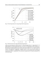
Fig.3. This can be understood from the validity of the constant mobility assumption.
Experimental data have shown that mobility is actually a function of V
GS
(Takagi et al.,
1994).
From Fig.7,
μ
eff
first increases with increasing V
GS
owing to Coulombic scattering and
then decreases owing to phonon scattering and surface roughness scattering. To further
investigate, we measured the I
ds
versus V
DS
characteristics and the I
ds
versus V
GS
characteristics of a long-channel NMOS transistor. Considering equal V
GS
step, we observed
an increasing spacing for 1 V≤ V
GS
≤ 3 V but constant spacing for 3 V ≤ V
GS
≤ 5V in the
saturation I
ds
versus V
DS
characteristics of the NMOS transistor (see Fig.8). Since the
transconductance (g
m
) is a measure of the low-field mobility (
μ
eff
) (Schroder, 1998), the g
m
versus V
GS
characteristics is expected to have the same features as the mobility versus V
GS
characteristics. From Fig. 8(a), the drain current saturation of the NMOS transistor occurs at
V
DS
around 3 V. With reference to Fig. 8(b), when V
DS
= 3 V and 0 V ≤ V
GS
≤ 3 V, g
m
increases
monotonically with increasing V
GS
owing to Coulombic scattering. When V
GS
is further
increased to beyond 3 V, surface roughness scattering will start to dominate and then g
m
will
decrease with increasing V
GS
. Hence, for 1 V ≤ V
GS
≤ 3 V, the saturation I
ds
versus V
DS
characteristics has increasing spacing for equal V
GS
step. For 3 V ≤ V
GS
≤ 5 V, the saturation
I
ds
versus V
DS
characteristics has constant spacing for equal V
GS
step. Since velocity
saturation does not occur in long channel transistor, the constant spacing observed in the
saturation I
ds
versus V
DS
characteristics at high V
GS
cannot be used as an indicator of the
onset of velocity saturation.
Low-field mobility,
μ
eff
Phonon
scattering
Surface
roughness
scattering
Coulombic
scattering
Gate-to-source voltage, V
GS
Low-field mobility,
μ
eff
Phonon
scattering
Surface
roughness
scattering
Coulombic
scattering
Gate-to-source voltage, V
GS
Fig. 7. Effects of the scattering mechanisms on the
μ
eff
versus V
GS
characteristics of MOS
transistor.
Solid State Circuits Technologies
58
Fig. 8. Constant spacing is observed in the saturation I
ds
versus V
DS
characteristics of a
NMOS transistor (L = 10 μm, W = 10 μm, physical gate oxide thickness of 300 Å) for equal
V
GS
step.
Here, it is interesting to note that it is common for the saturation I
ds
versus V
DS
characteristics of the zinc oxide thin-film transistors to have increasing spacing for equal V
GS
step (Cheong et al., 2009; Yaglioglu et al., 2005). The mobility of these materials ( ~ 10 to 20
cm
2
/V.s) is only one tenth of the mobility of silicon (~ 100 to 300 cm
2
/Vs). In Fig.9, which is
modified from (Cheong et al., 2009), the drain current saturation occurs at V
DS
around 15 V.
The increasing spacing observed in the saturation I
ds
versus V
DS
characteristics of the thin-
Fig. 9. Zinc oxide thin-film transistors with L = 20 μm and W = 40 μm (a) Increasing spacing
observed in the experimental I
ds
versus V
DS
characteristics of, (b) Monotonically increasing
g
m
. Modified from (Cheong et al., 2009).
The Evolution of Theory on Drain Current Saturation Mechanism
of MOSFETs from the Early Days to the Present Day
59
film transistor is related to the monotonically increasing g
m
with increasing V
GS
. Next, we
will study the dependency of the saturation I
ds
of the thin film transistor on V
GS
. From Fig.
10, if I
ds
and V
GS
have linear dependency, V
th,sat
extracted by linear interpolation is around
17.5 V. If I
ds
and V
GS
have quadratic dependency, V
th,sat
extracted by extrapolating the linear
portion of the I
ds
0.5
versus V
GS
plot is around 10 V. As seen in the I
ds
versus V
DS
characteristics of the thin-film transistor (see Fig.9), the transistor is in cutoff mode when V
GS
≤ 10 V. Hence, it is more appropriate to say that I
ds
of thin-film transistor and V
GS
have
quadratic dependency rather than linear dependency.
Fig. 10. Relationship between I
ds
and V
GS
of the zinc oxide thin-film transistors (L = 20 μm
and W = 40 μm) (a) Linear dependency (b) Quadratic dependency. Modified from (Cheong
et al., 2009).
4. Newer theories on the saturation drain current
equations of the nanoscale
MOS transistor
According to (Natori, 2008), the type of carrier transport in the MOS transistor depends on
the relative dimension between the gate length (L) and the mean free path (
λ
), as illustrated
in Fig. 11. Qualitatively,
λ
is the average distance covered by the channel carrier between the
successive collisions. When L is much bigger than
λ
, the channel carriers will experience
diffusive transport. When L is comparable to
λ
, the carriers undergo only a small number of
scattering events from the source to the drain and thus the carriers will experience quasi-
ballistic transport. Ballistic transport will only occur when L < λ. The experimentally
extracted
λ
is in the range of 10 nm for the nanoscale transistor (M-J. Chen et al., 2004; Barral
et al., 2009). Hence, the state-of-the-art MOS transistor (L ≥ 32 nm) is more likely to
experience quasi-ballistic transport rather than ballistic transport. This section will discuss
the main concepts of ballistic transport and then proceed to discuss about the existing quasi-
ballistic theories. The emphasis of this section is to introduce a simplified equation for the
saturation drain current of the nanoscale MOS transistor that is able to address quasi-
ballistic transport while having electrical parameters that are obtainable from the standard
Solid State Circuits Technologies
60
device measurements. Here, we will introduce two equations that can satisfy the above
criteria (i) Based on the concept of the effective saturation velocity (v
sat_eff
) , which is a
function of
μ
eff
and temperature (Lau et al. , 2008, b) and (ii) Based on the virtual source
model (Khakifirooz et al., 2009).
Case 3: L <
λ
Ballistic transport
Drain
Gate length, L
Case 1: L >>
λ
Diffusive transport
Case 2: L ~
λ
Quasi-Ballistic transport
Source
Case 3: L <
λ
Ballistic transport
Drain
Gate length, L
Case 1: L >>
λ
Diffusive transport
Case 2: L ~
λ
Quasi-Ballistic transport
Source
Fig. 11. Types of carrier transport in MOS transistors, which is modified from Fig. 1 in
(Natori, 2008). Note that
λ
is the mean free path of the carrier.
4.1 Ballistic transport
In vacuum, electrons will move under the influence of electric field according to Newton’s
second law of motion,
e
Fma qE
=
=− (9)
where F, m
e
, a, q and E are the resultant force acting on the electron, the electron mass, the
acceleration of the electron, the electronic charge , and the electric field ,respectively. Under
such a situation, if the applied electric field is constant in both magnitude and direction, the
electrons will accelerate in the direction opposite to that of the electric field. This type of
transport is known as the ballistic transport. In the other words, if there is no obstacle to
scatter the electrons, the electrons will experience ballistic transport (Heiblum & Eastman,
1987). Furthermore, (Bloch, 1928) postulated that the wave-particle duality of electron
allows it to move without scattering in the densely packed atoms of a crystalline solid if (i)
the crystal lattice is perfect and (ii) there is no lattice vibration. However, doping impurities
such as boron, arsenic and phosphorus are added to the silicon crystal so as to tune the
electrical parameters such as the threshold voltage and the off-state current (I
off
). These
dopants will disrupt the periodic arrangement of the crystal lattice and thus results in
collisions with the impurity ions and the crystalline defects. Moreover, the atoms in crystals
are always in constant motion according to the Particle Theory of Matter. These thermal
vibrations cause waves of compression and expansion to move through the crystal and thus
scatter the electrons (Heiblum & Eastman, 1987).
Therefore, achieving ballistic transport in
Si-based MOS transistors is only an ideal situation (Natori, 2008).
The Evolution of Theory on Drain Current Saturation Mechanism
of MOSFETs from the Early Days to the Present Day
61
4.2 Quasi-ballistic transport
Having established that thermionic emission from the source to the channel is still relevant
in the state-of-the-art MOS transistor (L ≥ 32 nm) in Section 1, we will proceed to discuss the
main concepts behind quasi-ballistic transport. (Lundstrom, 1997) derived an equation that
relates the saturation I
ds
of the nanoscale transistor to
μ
eff
as follows,
()
ox
ds GS th,sat
T
eff
11
(0 )
CW
IVV
v
μ
ε
+
⎡⎤
⎢⎥
⎢⎥
=−
⎢⎥
+
⎢⎥
⎣⎦
(10)
where the random thermal velocity of the carriers (v
T
) does not depend V
GS
. The only
variable in the v
T
equation is the temperature (T).
()
()
TT
() 2 /
Bt
vvT kT m
π
== (11)
where the transverse electron mass of silicon (m
t
) is equal to 0.19 m
0
where the free electron
mass (m
0
) is equal to 9.11 × 10
-31
kg (Singh, 1993). Using equation (11), v
T
is approximately
equal to 1.2 × 10
7
cm/s at temperature of 25 °C. k
B
is the Boltzmann constant. T is the
absolute temperature. ε(0
+
) is defined as the average electric field within the length ℓ where
a k
B
T/q potential drop occurs, as shown in Fig.12 in (Lundstrom & Ren, 2002). Despite the
lack of equation for ε(0
+
) (Lundstrom, 1997; Lundstrom & Ren, 2002), Lundstrom has made
an important contribution to relate the low-field mobility (
μ
eff
) to I
on
of the deep submicron
MOS transistors, and thus his theory is able to account for the strain-induced enhancement
in I
on
(Yang et al., 2004; C-H. Chen et al., 2004; Yang et al. 2008; Wang et al., 2007).
According to (Lundstrom, 1997), if a carrier backscatters beyond ℓ, it is likely to exit from the
drain and is unlikely to return back to the source (see Fig. 12). For NMOS transistor, ℓ is the
distance between the top of the conduction band edge and the point along the channel
where channel potential drops by k
B
T/q.
k
B
T / q
Source
Drain
Channel
electron
0
x
E
C
k
B
T / q
Source
Drain
Channel
electron
0
x
E
C
Fig. 12. Definition of the critical length (ℓ) for NMOS transistor. ℓ is defined to be the distance
between the top of the conduction band edge and the point along the channel where channel
potential drops by k
B
T/q. Beyond ℓ, the carriers are unlikely to return to the source.
Solid State Circuits Technologies
62
By inspection of equations (10) and (11), a loop-hole can be found in Lundstrom’s 1997
theory. If equations (10) and (11) are correct, MOS transistors will function very poorly
when the temperature is lowered from room temperature to very low temperature such as
liquid helium temperature. However, there are numerous reports that MOS transistors and
CMOS integrated circuits can function quite well at the liquid helium temperature (Chou et
al., 1985; Ghibaudo & Balestra, 1997; Yoshikawa et al., 2005). Hence, there is a need to
modify Lundstrom’s 1997 theory. Indeed, (Lundstrom & Ren, 2002) made an attempt to
incorporate Natori’s 1994 theory into their theory. However, the resulting theory is very
much not similar to equation (10) and has not been compared with real device performance.
Based on equation (24) in (Natori, 1994),
the saturation drain current of the nanoscale MOS
transistor is as follows,
()
3/2
ox GS th,sat
ds
tv
8-
3
WC V V
I
mqM
π
⎡⎤
⎣⎦
=
=
(12a)
where ħ is the reduced Planck’s constant. M
v
is the product of the lowest valley degeneracy
and the reciprocal of the fraction of the carrier population in the lowest energy level. For a
NMOS transistor that is fabricated on (100) Si substrate, the fraction of the carrier
population at the strong inversion is around 0.8 at 77 K but it decreases to around 0.4 at 300
K (Stern, 1972). In the other words, M
v
is a function of temperature (T).
Rearranging equation (12a) results in,
()
ox
ds GS th,sat
inj GS
1
(,)
CW
IVV
vV T
⎡⎤
⎢⎥
⎢⎥
=−
⎢⎥
⎢⎥
⎣⎦
(12b)
where the injection velocity (v
inj
) is given by (Natori, 1994 ),
()
ox GS th,sat
inj GS
tv
8-
(,)
3()
CVV
vV T
mqMT
π
=
=
(12c)
With reference to Fig.8 in (Natori, 1994 ), v
inj
increases with increasing temperature (T) and
increasing V
GS
. If Natori’s theory is true, v
inj
can be very high even though the temperature
is very low. We propose that this feature of Natori’s 1994 theory can be used to cover the
shortcomings of Lundstrom’s 1997 theory. However, there are some aspects of Natori’s 1994
theory that contradict the experimental data. From Fig. 8 in (Natori, 1994), his theory, which
disregards the channel scattering, predicted that the saturation I
ds
of the nanoscale NMOS
transistor will increase when temperature increases. However, this is contradictory to the
experimental data. Fig. 13 shows that the experimental I
ds
of a NMOS transistor (L= 60 nm)
actually decreases when temperature increases. This can be explained by the increase in
channel scattering when temperature increases (Takagi et al., 1994; Kondo & Tanimoto,
2001; Mazzoni et al., 1999). Moreover, equation (12b) cannot account for the strain-induced
enhancement in I
on
(Yang et al, 2004; C-H. Chen et al, 2004; Yang et al., 2008; Wang et al.,
2007). Hence, without the help of Lundstrom’s 1997 theory, Natori’s 1994 theory is
contradictory to the experimental data.
The Evolution of Theory on Drain Current Saturation Mechanism
of MOSFETs from the Early Days to the Present Day
63
In addition, Natori’s 1994 theory predicts that the saturation I
ds
of the nanoscale MOS
transistors will follow a (V
GS
– V
th,sat
)
3/2
relationship. Fig. 14a shows the saturation I
ds
2/3
versus V
GS
characteristics of a NMOS transistor (L = 60 nm). The threshold voltage extracted
by the linear extrapolation is smaller than the threshold voltage of conduction. This shows
that the saturation I
ds
of the nanoscale MOS transistors does not follow a (V
GS
– V
th,sat
)
3/2
relationship. Fig. 14b shows the saturation I
ds
versus V
GS
characteristics of the same NMOS
transistor. In this case, the extracted threshold voltage is close to the threshold voltage of
conduction. Hence, the saturation I
ds
of nanoscale transistors is more likely to follow a (V
GS
–
V
th,sat
) relationship.
Fig. 13. Effects of temperature on the saturation I
ds
versus V
GS
characteristics of a NMOS
transistor (L = 60 nm, W = 5 μm).
Fig. 14. As opposed to Natori’s 1994 theory, the saturation I
ds
of the short channel NMOS
transistor does not follow a (V
GS
– V
th,sat
)
3/2
relationship.
Solid State Circuits Technologies
64
4.3 New equation that unifies Natori’s 1994 theory and Lundstrom’s 1997 theory
We propose a simplified equation that can unify both Natori’s 1994 theory and Lundstrom’s
1997 theory, as follows (Lau et al., 2008, b),
()
ox
ds GS th,sat
1GS 1GS
11
(,) (,)
CW
IVV
vV T vV T
⎡⎤
⎢⎥
⎢⎥
=−
⎢⎥
+
⎢⎥
⎣⎦
(13)
where
(
)
(
)
1GS injGS
, , vV T v V T=
(14)
()()
(
)
2GS effGS
, , 0vV T V T
με
+
= (15)
(Lundstrom, 1997) proposed that v
1
is equal to v
T
that is only dependent on T, as shown in
equation (11). On the other hand, our theory proposed that v
1
is a function of both V
GS
and
T, and v
1
can be higher than v
T
given by equation (11). (Natori, 1994)
proposed that v
1
is
equal to v
inj
, which is a function of both V
GS
and T. Recently, (Natori et al., 2003; Natori et
al., 2005) simulated the v
inj
characteristics using the multi-subband model (MSM). In weak
inversion, v
inj
is almost independent of V
GS
and is approximately equal to 1.2 x 10
7
cm/s,
which is equal to v
T
. In strong inversion, v
inj
will increase due to carrier degeneration but is
confined within a narrow range from 1.2 x 10
7
cm/s to 1.6 x 10
7
cm/s.
Here, we would like to highlight that both Lundstrom’s 1997 theory and Natori’s 1994
theory did not consider the series resistance (R
sd
). Although the conduction band edge (E
c
)
profile in the n-channel will be the same with or without R
sd
(Martinie et al., 2008), the E
c
within S/D regions will be different when the effects of R
sd
is considered. If the effects of R
sd
are disregarded, E
c
within S/D regions will appear as a horizontal line, as illustrated in Fig.
12. However, the presence of R
sd
will cause a potential drop in the S/D regions, resulting in
a built-in electric field within the S/D regions (see Fig. 15). This electric field in the source
region will accelerate the electrons. Since scattering decreases when temperature decreases
(Takagi et al., 1994; Kondo & Tanimoto, 2001; Mazzoni et al., 1999), one would expect that
there will be minimal scattering in the source when the temperature is very low. Hence, the
presence of R
sd
will allow the electrons to attain higher energy prior to thermionic emission
into the channel. According to (M-J. Chen et al., 2004), the source series resistance (R
s
) is
about 75 Ω-µm. If the drain current (I
ds
) is about 800 μA/μm, the voltage drop due to R
s
is
about 800 μA/μm x 75 Ω-µm = 60 mV. (Note that the thermal voltage, k
B
T/q is
approximately 26 meV at room temperature.) We proposed that the electrons are “heated”
up by the 60 meV energy due to R
sd
and thus their velocities can be significantly larger than
1.2 x 10
7
cm/s (as predicted by equation 12c). Moreover, this extra energy is expected to
increase with increasing V
GS
because higher V
GS
implies a bigger I
ds
. With this extra energy
from electron heating in the R
sd
region, the carriers can overcome the potential barrier at the
liquid nitrogen temperature despite not being able to gain energy from the surrounding.
The significance of v
2
term is that it establishes a link between I
on
and
μ
eff
. This provides a
better compatibility between theory and I
on
enhancement in the nanoscale transistors by
various stress engineering techniques (Yang et al., 2004; C-H. Chen et al., 2004; Yang et al.,
The Evolution of Theory on Drain Current Saturation Mechanism
of MOSFETs from the Early Days to the Present Day
65
2008; Wang et al., 2007). However, there is no v
2
term in Natori’s 1994 theory, as shown in
equation (12b). Nevertheless, v
2
is covered by Lundstrom’s 1997 theory, as shown in
equation (10). Hence, we incorporate v
2
in Lundstrom’s 1997 theory into equation (13).
Source DrainChannel
Thermionic
emission
electron
Source DrainChannel
Thermionic
emission
electron
Fig. 15. The effects of S/D series resistance on the conduction band edge of a NMOS
transistor in the saturation operation.
Another loop-hole in Lundstrom’s 1997 theory
is that there is no equation for ε(0
+
)
.
From
Fig.9 in (M-J. Chen et al., 2004), the slope of the near-source channel conduction band
increases when V
GS
increases. In the other words, the electric field near the top of potential
barrier, ε(0
+
) increases with increasing V
GS
. Hence, we deduce that ε(0
+
) is a function of both
V
GS
and V
DS
such that ε(0
+
, V
GS
, V
DS
= V
DD
) is approximately equal to ε(0
+
, V
GS
, V
DS
= V
Dsat
).
Note that V
DD
is the power supply voltage. This is consistent with Fig. 5 in (Fuchs et al.,
2005).
Therefore, we propose that ε(0
+
) can be expressed as follows,
1Dsat
eff
(0 )
V
L
α
ε
+
= (16a)
where the correction factor (
α
1
) is smaller than 1. Based on the conventional MOS transistor
theory (Taur & Ning, 1998, a), V
Dsat
is given by (V
GS
– V
th,sat
)/m where 1.1 ≤ m ≤ 1.4.
Furthermore, (Suzuki & Usuki, 2004) proposed a drain current model that shows that V
Dsat
is
smaller than (V
GS
– V
th,sat
) for the short-channel MOS transistors.
This shows that the
relationship of V
Dsat
= (V
GS
– V
th,sat
)/m is still reasonably correct for very short MOS
transistors. Therefore, ε(0
+
) can also be expressed by,.
(
)
2GS th,sat
eff
(0 )
VV
L
α
ε
+
−
= (16b)
where the correction factor (
α
2
) is smaller than 1. The value of
α
2
can be estimated from the
effective carrier velocity (v
eff
) versus V
GS
characteristics and the
μ
eff
versus V
GS
characteristics. Using the saturated transconductance method suggested by (Lochtefeld et
al., 2002), v
eff
was extracted as a function of V
GS
as shown in Fig.16 (a). For the contact etch
stop layer (CESL) with a tensile stress of 1.2 GPa, ν
sat_eff
of the NMOS transistor (L = 60 nm)
was
7.3 × 10
6
cm/s. Using the constant current method with reference current, I
ref
Solid State Circuits Technologies
66
=0.1μA(W/L) , the extracted V
th,sat
was about 0.3 V. Next, L
eff
, which is extracted using the
method proposed by (Guo et al., 1994)
, was about 0.030 μm. Substituting L
eff
= 3 x 10
-6
cm,
V
GS
= 1.2 V , V
th,sat
= 0.3 V into equation (16b),
(
)
5
2
0 3 10 (in units of V/cm)
εα
+
=× (16c)
Re-arranging ν
sat_eff
=
μ
eff
ε(0
+
) ,
sat_eff
eff
(0 )
v
ε
μ
+
= (16d)
Next,
μ
eff
is extracted as a function of V
GS
using a method described by (Schroder, 1998).
From Fig. 16(b), when V
GS
is 1.2 V,
μ
eff
was about 85 cm
2
V
-1
s
-1
at. Substituting ν
sat_eff
= 7.3
×10
6
cm/s and
μ
eff
= 85 cm
2
V
-1
s
-1
into equation (16d),
6
sat_eff
4
eff
7.3 10
(0 ) 8.588 10 V/cm
85
v
ε
μ
+
×
== =× (16e)
According to (Lee et al., 2009), ε(0
+
)of a PMOS transistor (L = 50 nm) is between 8 ×10
4
V/cm
and 3 ×10
5
V/cm for various gate overdrives. By solving equations (16c) and (16e),
α
2
is
around 0.29. Note that
α
2
is 0.5 for the conventional MOS transistor theory (Taur & Ning,
1998, a).
Fig. 16. Effects of uniaxial tensile stress on (a) the v
eff
versus V
GS
characteristics, (b) the
μ
eff
versus V
GS
characteristics of a NMOS transistor (L = 60 nm, W = 0.12 μm). Note v
sat_eff
is the
average value of v
eff
when V
GS
is close to V
DD
. The uniaxial tensile stress is induced by the
contact etch stop layer (CESL). The film stress of the two CESL split are 0.7 GPa tensile stress
and 1.2 GPa tensile stress.
Equation (13) is then modified by defining a new parameter called the effective carrier
velocity (ν
eff
). The resulting equation is as follows (Yang et al., 2007; Lau et al., 2008, a; Lau et
al., 2008, b),
The Evolution of Theory on Drain Current Saturation Mechanism
of MOSFETs from the Early Days to the Present Day
67
(
)
ds eff eff GS ox GS th,sat
(,,)Iv VTWCVV
μ
=− (17)
where v
eff
is a function of
μ
eff
, V
GS
and T at a constant V
DS
(see Fig.16a and Fig.17).
Furthermore, v
eff
is also related to v
1
and v
2
, as follows,
1
eff eff GS
1GS 2effGS
11
(,,T)
(,) (,,)
vV
vV T v V T
μ
μ
−
⎛⎞
=+
⎜⎟
⎝⎠
(18)
When temperature decreases, v
inj
decreases (Natori, 1994). Since v
1
is related to v
inj
(see
equation 14), v
1
is expected to decrease with decreasing temperature. On the other hand,
mobilities due to Coulombic scattering, phonon scattering and surface roughness scattering
will increase with decreasing temperature (Takagi et al., 1994; Kondo & Tanimoto, 2001;
Mazzoni et al., 1999). As v
2
is related to
μ
eff
(see equation 15), we expect v
2
to increase when
temperature decreases. Fig. 17 shows that the experimental v
eff
increases when temperature
decreases, and hence v
2
dominates over v
1
.
Fig. 17. The effect of temperature on v
sat_eff
. Note that v
sat_eff
corresponds to the average
value of v
eff
when V
GS
is close to V
DD
(L = 60 nm, W = 5 μm, V
DS
= V
DD
= 1.2 V).
Another evidence to illustrate the importance of v
2
over v
1
is through their behavior with
V
GS
. Fig.18 shows the behavior of v
1
, v
2 ,
v
eff
with V
GS
.
Since v
1
is related to v
inj
, v
1
is expected
to increase when V
GS
increases (Natori, 1994). On the other hand, v
2
is related to
μ
eff,
as
shown in equation (15). Hence, the v
2
versus V
GS
characteristics will tend to follow that of
the
μ
eff
versus V
GS
characteristics (see Fig. 7). When V
GS
is low, v
2
is expected to increase with
increasing V
GS
owing to the screening of the Coulombic scattering centres. When V
GS
is high,
an increase in V
GS
will decrease
μ
eff
owing to the surface roughness scattering. From
equation (15), v
2
is the product of
μ
eff
and
ε
(0
+
). From equation (16b),
ε
(0
+
) is expected to
increase with increasing V
GS
. Hence, v
2
is expected to approach a constant at high V
GS
owing
to the opposing effects of
μ
eff
and
ε
(0
+
).
Solid State Circuits Technologies
68
Gate voltage , V
GS
Velocity components
v
1
= v
inj
v
2
=
μ
eff
ε(0
+
)
v
eff
= (1/v
1
+ 1/v
2
)
-1
Fig. 18. A schematic diagram showing the relationship of v
1
, v
2
and v
eff
with V
GS
.
Since ν
eff
approaches a constant when V
GS
close to V
DD
(see Fig. 16a and Fig. 17), it is more
appropriate to replace v
eff
in equation (17) can be replaced by ν
sat_eff
, resulting in (Yang et al.,
2007; Lau et al., 2008,a; Lau et al., 2008,b
),
(
)
ds sat_eff eff ox,inv GS th,sat_IV
(,)Iv TWC VV
μ
=− (19)
where v
sat_eff
is the average value of v
eff
when V
GS
is close to V
DD
. In Fig. 16(a), v
sat_eff
increases when tensile stress increases, and thus leads to I
on
enhancement in the short
channel NMOS transistor. This shows that equation (19) is able to account for the strain-
induced I
on
enhancement by various strain engineering techniques (Yang et al., 2004; C-H.
Chen et al., 2004; Yang et al. 2008; Wang et al., 2007). As shown in Fig.17, v
sat_eff
increases
when temperature decreases, resulting in a better I
on
performance at very low temperature.
This shows that equation (19) is able to explain the I
on
enhancement at liquid helium
temperature (Chou et al., 1985; Ghibaudo & Balestra, 1997; Yoshikawa et al., 2005).
Fig. 19. Extraction of V
th,sat_IV
from the saturation I
ds
versus V
GS
characteristics of a NMOS
transistor (L = 60 nm, W = 2 μm, V
DS
= 1.2 V).
The Evolution of Theory on Drain Current Saturation Mechanism
of MOSFETs from the Early Days to the Present Day
69
Moreover, V
th,sat
in equation (17) needs to be replaced by V
th,sat_IV
. As illustrated in Fig. 19,
V
th,sat_IV
can be extracted from the saturation I
ds
versus V
GS
characteristics. First, a best-fit
line is performed on the saturation I
ds
versus V
GS
characteristics whenV
GS
is close to V
DD
.
For our transistors, v
eff
approaches a constant when 1 V ≤ V
GS
≤ 1.2 V. V
th,sat_IV
can be found
by the interception between the best-fit line and the V
GS
axis. In this example, V
th,sat_IV
was
0.603 V. For comparison, we extracted V
th,sat
using the Constant Current (CC) method with
the reference drain current (I
ref
) defined as 0.1μA(W/L). The extracted V
th,sat
was 0.351 V,
which is much smaller than V
th,sat_IV
. Moreover, we also observed that V
th,sat_IV
is also bigger
than the linear threshold voltage (V
th,lin
). In Fig. 20(a), V
th,lin
extracted using CC method was
0.484 V. In Fig. 20(b), V
th,lin
extracted using maximum g
m
method was 0.557 V. We believe
that V
th,sat_IV
is bigger than V
th,lin
and V
th,sat
because it accounts for the additional V
GS
that is
required to produce electrons to screen the Coulombic scattering centres, as shown in Fig.
21. On the other hand, V
th,lin
and V
th,sat
indicate the onset of inversion. Furthermore,
polysilicon depletion and quantum mechanical effects will make the gate oxide appears
thicker, and thus C
ox
in equation (17) has to be replaced by C
ox,inv
, which is the gate oxide
capacitance per unit area at inversion.
4.4 Virtual source model for nanoscale transistors in saturation mode
(Khakifirooz et al., 2009) proposed a semi-empirical model for the saturation drain current
of the nanoscale transistor. This model is based on the location of the “virtual source”,
which is the top of the conduction band profile for NMOS transistor, as shown in Fig. 22.
Based on the “charge-sheet approximation”, the saturation I
ds
of the nanoscale transistor can
be described by the product of the local charge density and the carrier velocity, as follows
(Khakifirooz & Antoniadis, 2008).
ds ixo xo
IWQv=
(20)
Fig. 20. Extraction of V
th,lin
of a NMOS transistor in the linear operation (L = 60 nm, W = 2
μm, V
DS
= 0.05 V) (a) Using constant current method with I
ref
= 0.1 μA W/L , V
th,lin
= 0.484 V,
(b) Using maximum g
m
method (V
th,lin
= 0.582 - V
DS
/2 = 0.557 V).
Solid State Circuits Technologies
70
Fig. 21. V
th,sat_IV
includes a component to overcome the Coulombic scattering by “screening”.
The virtual source charge density (Q
xio
) is given by (Khakifirooz et al., 2009),
GS ds s th,sat
B
xio ox
B
n1 exp
/
VIRV
kT
QC l
qmkTq
⎡
⎤
−−
⎛⎞
=+
⎢
⎥
⎜⎟
⎢
⎥
⎝⎠
⎣
⎦
(21)
where R
s
is the source series resistance. The body-effect coefficient (m) can be expressed as
(Taur & Ning, 1998,b),
()
0chB
ox
/4
1
Si
qN
m
C
εε ψ
=+ (22)
where ε
0
is the permittivity of free space. ε
Si
is the dielectric constant of silicon. N
ch
is the
channel doping concentration.
ψ
B
is the difference between the Fermi level in the channel
region and the intrinsic Fermi level.
The virtual source velocity (v
xo
) is the average velocity of the channel carriers at the potential
barrier near the source.
()
x0
ox s
112
v
v
CRW v
δ
=
−+
(23)
where δ is the drain-induced-barrier lowering (DIBL) with units of V/V. The carrier velocity
can be extracted as follows,
()
ds
ox GS th,sat
/
IW
v
CV V
=
−
(24)
According to (Khakifirooz et al., 2009), the above model has a reasonably good fit to the
experimental I
ds
versus V
GS
characteristics and the experimental I
ds
versus V
DS
characteristics
of nanoscale Si-based MOS transistors fabricated using poly-SiON gate stack as well as high-
The Evolution of Theory on Drain Current Saturation Mechanism
of MOSFETs from the Early Days to the Present Day
71
K metal gate stack. The extracted v
xo
for NMOS transistor (L = 35 nm) is around 1.4×10
7
cm/s. Since v
sat
for electrons in silicon is 10
7
cm/s (Norris & Gibbons, 1967), this shows that
velocity saturation does not occur in the nanoscale Si-based MOS transistor.
V
GS
> V
th,sat
V
D
V
S
R
s
R
D
Q
ix0
x
0 x
0
E
c
Source
Drain
v
x0
L
V
GS
> V
th,sat
V
D
V
S
R
s
R
D
V
GS
> V
th,sat
V
D
V
S
R
s
R
D
Q
ix0
x
0 x
0
E
c
Source
Drain
v
x0
L
Fig. 22. Illustration of the virtual source point (x
0
) in a NMOS transistor. The carrier charge
density (Q
ixo
) and the virtual velocity (v
xo
) are defined at the top of the conduction band
profile along the channel direction. R
s
is the source series resistance. R
D
is the drain series
resistance.
5. Apparent velocity saturation in the nanoscale MOS transistor
Fig. 23 shows the maximum
μ
eff
versus L characteristics and the v
sat_eff
versus L
characteristics of a bulk NMOS transistor.
μ
eff
is extracted from the linear I
ds
versus V
GS
characteristics (Schroder, 1998).
v
eff
is extracted using the saturation transconductance
method (Lochtefeld et al., 2002). R
sd
correction to v
eff
has to be done as described by (Chou &
Antoniadis, 1987) .
R
sd
is extracted using a modified version of the method according to
(Chern et al., 1980). Note that v
sat_eff
is the average value of v
eff
when V
GS
is close to V
DD
. By
taking the maximum
μ
eff
to be independent of the gate length, v
sat_eff
= constant x L
eff
–1
,
based on equation (16b) and equation (16d). However, the experimental v
sat_eff
= constant x
L
eff
–β
where β is less than 1 despite the uncertainty in R
sd
measurements (see Fig. 24). This
indicates that the carrier velocity tends to saturate when L decreases (see Fig. 23b).
Since the relationship between the carrier velocity and the low-field mobility is well-
established (Khakifirooz & Antoniadis, 2006), we can have a better understanding of the
apparent velocity saturation in the nanoscale MOS transistors by looking at the mobility. A
strong reduction of mobility is typically observed in the silicon-based MOS transistors when
the gate length is scaled (Romanjek et al., 2004; Cros et al., 2006; Cassé et al., 2009; Huet et
al., 2008; Fischetti & Laux, 2001). The reason of this degradation is still not clearly
understood. It is first attributed to the halo implants as its contribution to the channel
doping concentration increases with decreasing gate length (Romanjek et al., 2004).
However, this mobility degradation is also observed in the undoped double gate MOS
Solid State Circuits Technologies
72
Fig. 23. Effects of scaling on bulk NMOS transistors (W = 1 μm) (a) the
μ
eff
versus L
characteristics, (b) the v
sat_eff
versus L characteristics. Note that v
sat_eff
increases with
increasing
μ
eff
. R
sd
= 0 Ω-μm refers to the case where R
sd
correction is not performed.
Fig. 24. Validity of v
sat_eff
= constant x L
eff
–β
where β is less than 1 despite the uncertainty in
R
sd
measurements. Note that log v
sat_eff
= -βlog L
eff
+ log constant.
transistors (Cros et al., 2006) and the undoped fully-depleted silicon-on-insulator (FD-SOI)
MOS transistors (Cassé et al., 2009). This indicates that the halo implant is not the dominant
factor involved in the degradation. Another limiting transport mechanism expected to be
non-negligible in the short-channel MOS transistor is the presence of crystalline defects
induced by S/D extension implants (Cros et al., 2006). Furthermore, Monte Carlo studies
shows that ballistic transport has significant impact on the mobility degradation (Huet et al.,
2008). Another explanation is that the increase in the long-range Coulombic scattering
interactions between the high-density electron gases in the S/D regions and the channel
electrons for very short channel MOS transistors (Fischetti & Laux, 2001).
In an attempt to
clarify the mobility degradation mechanism, (Cassé et al., 2009) used the differential
The Evolution of Theory on Drain Current Saturation Mechanism
of MOSFETs from the Early Days to the Present Day
73
magnetoresistance technique for mobility extraction to eliminate the effects of series
resistance (R
sd
) and the ballisticity introduced by L-independent resistance. However, strong
mobility degradation is still observed in the undoped FD-SOI MOS transistors (L < 100 nm)
at 20 K and thus the mobility degradation is likely to be caused by (i) the long-range
Coulombic scattering interactions between the electron gases in the S/D regions and the
channel electrons, (ii) the charged defects at the S/D regions, and (iii) the neutral defects at
the S/D regions (Cassé et al., 2009).
The apparent saturation of carrier velocity when L
decreases can be understood as follows. As discussed in section 4.3, the effects of v
2
dominates over the effects of v
1
such as v
eff
≈ v
2
. From equation (15), v
2
is the product of
μ
eff
and ε(0
+
). From equation (16b), ε(0
+
) increases when L
eff
decreases. In short, when L
decreases,
μ
eff
decreases but ε(0
+
) increases. Hence, v
eff
is expected to approach a constant
when L decreases. Since v
sat_eff
is the average value of v
eff
when V
GS
is close to V
DD
, v
sat_eff
is
expected to approach a constant when L decreases. This is probably why (Hauser, 2005) is
able to use the velocity saturation model (see equation 5) to fit the experimental I
ds
versus
V
DS
characteristics of the nanoscale NMOS transistor (L = 90 nm). Note that Hauser used v
sat
as a fitting parameter. In his physics-based model, v
sat
is taken to be 2.06×10
7
cm/s rather
than 1 × 10
7
cm/s (saturation velocity of electrons in silicon at room temperature). Therefore,
the physics behind the apparent saturation of the carrier velocity is different from that of
velocity saturation (the rate of energy gain from the lateral electric field is equal to the rate
of energy loss to the surroundings by phonon scattering).
6. Drain current saturation mechanism of the nanoscale MOS transistors
As mentioned in section 2, the two well-known mechanisms for drain current saturation in
MOS transistors are pinch off and velocity saturation. However, we have shown that
velocity saturation is unlikely to occur in the nanoscale MOS transistors. In addition, (Kim et
al., 2008) reported that the experimental observation of velocity overshoot in the nanoscale
bulk NMOS transistor (L = 36 nm) at room temperature. In section 5, we have unveiled that
the apparent velocity saturation that occurs during scaling is caused by (i) the long-range
Coulombic scattering interactions between the electron gases in the S/D regions and the
channel electrons, (ii) the charged defects at the S/D regions and (iii) the neutral defects at
the S/D regions (Cassé et al. 2009). Since velocity saturation involves the tradeoff between
the rate of energy gain from lateral electric field and the rate of energy loss to the
surroundings by phonon scattering, we believe that velocity saturation does not occur in the
nanoscale transistors. Hence, it is possible that the drain current saturation mechanism in
nanoscale MOS transistor is caused by pinch off rather than velocity saturation. In fact,
several groups of researchers have developed compact models for the pinch-off region of
the nanoscale MOS transistors (Navarro et al., 2005; Weidemann et al., 2007). For V
DD
= 1 V,
the pinch-off point is less than 10 nm from the drain side (Navarro et al., 2005). This shows
that the pinch-off point will always remain within the channel even though this point tends
to shift towards the source side with increasing V
DS
.
Our previous work gives the experimental evidence that the drain current saturation in the
nanoscale NMOS transistor is caused by pinchoff (Lau et al., 2009). By simply changing the
polarity of the drain bias (V
D
), it is possible to create a situation whereby pinchoff is unlikely
to occur. As shown in Fig. 25, the normal biasing involves the application of a positive V
D
to
the drain terminal of a NMOS transistor. On the other hand, the unusual biasing involves
Solid State Circuits Technologies
74
the application of a negative V
D
to the drain terminal of a NMOS transistor. The most
obvious implication of such biasing is the direction of the electron flow. For the normal
biasing condition, the electrons are injected from source terminal to drain terminal. For the
unusual biasing condition, the electrons are injected from drain terminal to source terminal.
In the other words, the effective source terminal for the unusual biasing is actually the drain
terminal. To avoid confusion, we define V
GS
*
as the potential difference between the gate
terminal and the terminal that injects electrons into the channel. V
DS
*
is the potential
difference between the source terminal and drain terminal. From equation (8), the condition
for pinchoff to occur is as follows,
*
GS th,sat
*
DS
VV
V
m
−
≥
(25)
where m is between 1.1 and 1.4 (Taur & Ning, 1998,a). For our NMOS transistors, V
DD
is 1.2
V. Under the normal biasing, V
GS
*
is 1.2 V and V
DS
*
is 1.2 V (see Fig. 25a). Under the unusual
biasing, V
GS
*
is 2.4 V and V
DS
*
is 1.2 V (see Fig. 25b). Hence, normal biasing will be able to
satisfy the condition for pinchoff and thus pinchoff can occur. However, the condition for
pinchoff cannot be satisfied under the unusual biasing because V
GS
* is much bigger than
V
DS
*. From Fig.26, the nanoscale NMOS transistor (L = 45 nm) used in our study does not
suffer from punchthrough. Note that negative V
D
will forward bias the p-well-to-n
+
drain
junction. To minimize the amount of forward biased p-n junction current in NMOS
transistor under the unusual biasing, we limited the V
D
to be -0.4 V (see Fig. 27). As shown
Fig. 25. Biasing conditions of the NMOS transistor (a) Under the normal biasing, a positive
V
D
of 1.2 V is applied to the drain terminal. The p-well-to-n
+
drain junction is reversed
biased. (b) Under the unusual biasing condition, a negative V
D
of -1.2 V is applied to the
drain terminal. The p-well-to-n
+
drain junction is forward biased.
The Evolution of Theory on Drain Current Saturation Mechanism
of MOSFETs from the Early Days to the Present Day
75
Fig. 26. The I
ds
versus V
GS
characteristics of the nanoscale NMOS transistor (L = 45 nm, W =
2 μm).
Fig. 27. Selection of the unusual V
D
biasing condition for NMOS transistor.
in Fig. 28, the application of V
D
= -0.4 V to the NMOS transistor will shift the I
ds
versus
V
GS
characteristics towards the left. If drain current saturation mechanism is caused by
velocity saturation, we will expect drain current saturation to occur in both normal V
D
biasing and unusual V
D
biasing. If drain current saturation mechanism is caused by
pinchoff, we will expect drain current saturation to occur in the normal V
D
biasing but not in
the unusual V
D
biasing. Fig. 29 shows that there is no obvious current saturation in the
experimental I
ds
versus V
DS
characteristics of the NMOS transistor under the unusual
biasing (negative V
D
).