Solid State Circuits Technologies Part 11 pdf
Bạn đang xem bản rút gọn của tài liệu. Xem và tải ngay bản đầy đủ của tài liệu tại đây (5.68 MB, 30 trang )
Solid State Circuits Technologies
292
Where, E’ and E are the transmitter energies in case of with and without misalignment,
respectively. Z’ and Z are the equivalent communication distances with and without
misalignment, respectively. D is the average between outer and inner diameter of inductors.
ΔX and ΔY are the values of misalignment in X-axis and Y-axis, respectively.
Figure 15 shows the total transmitter energy dependence on the angle of the inductor where
the misalignment value, ΔR is constant. The diameter and communication distance are 80μm
and 70μm. respectively. As shown in this figure, the difference of transmitter energy for all
angles is less than 5%. This result shows that proposed modeling can be applied to not only
1D analysis but also 2D analysis.
Normalized Required Total Transmitter Energy
4530150
Angle, [degree]
θ
0.95
0.9
1
Δ
R
=
3
2
μ
m
Δ
R
=
8
μ
m
Δ
R
=
1
6
μ
m
R
Rx
Calculated by Equation (1)
D
=80
μ
m,
Z
=70
μ
m
4530150
Angle, [degree]
θ
0.95
0.9
1
Δ
R
=
3
2
μ
m
Δ
R
=
8
μ
m
Δ
R
=
1
6
μ
m
R
θ
Tx
D
=80
μ
m,
Z
=70
μ
m
R
ΔΔΔ
Fig. 15. Normalized total transmitter energy dependence the position of the inductor.
4.2 Estimation of transmitter energy under misalignment
From the above theoretical analysis, we can calculate the relationship between design
parameters and misalignment, which is shown in Fig. 16. By referring to this figure,
parameter design with taking misalignment into consideration becomes possible. In order to
determine the specific value of transmitter energy, we targeted the BER and timing margin.
However, the proposed model can be applied to any BER and timing margin by scaling the
transmitter energy calculated by (1). The reason is that misalignment affects only coupling
coefficiency and the relationship between BER, timing margin, transmitter energy and
coupling coefficient is introduced in (Miura et al., 2007). In Fig. 16, the region where (1) is
valid will be explained in the following discussion. As shown in Fig. 16, there are points
where magnetic filed lines change the vertical direction. If the directions of all magnetic field
lines in the receiver inductor are same, (1) is valid. Such points were calculated from the
© 2009 IEEE
An Inductive-Coupling Inter-Chip Link for High-Performance and Low-Power 3D System Integration
293
simulation by 3D electro-magnetic (EM) solver and plotted in Fig. 16. When Z/ΔX is more
than approximately 0.8, (1) gives accurate value and its accuracy is confirmed by comparing
with simulation results by EM solver and measurement results in the following sections.
Communication Distance Normalized by
Diameter, Z/D
0
0.6
0.8
1
0.2
0
Misalignment Normalized by Diameter, ΔX/D
Timing Margin=100ps
0.1 0.2 0.3 0.4 0.5
0.4
1
p
J
/
b
2
p
J
/
b
3
p
J
/
b
4
p
J
/
b
5
p
J
/
b
7
p
J
/
b
Invalid Region
BER=10
-10
,
6
p
J
/
b
Measured
(D=80μm
Z=70μm)
Measured
(D=160μm
Z=70μm)
Invalid RegionInvalid Region
Fig. 16. Relationship among energy dissipation, normalized misalignment and
communication distance.
4.3 Estimation of transmitter energy with consideration of crosstalk
Misalignment also affects the performance in array operation. In arrayed inductive-coupling
link, bit error rate is given by the following equation (Miura et al., 2007).
⎟
⎟
⎠
⎞
⎜
⎜
⎝
⎛
−−
=
N
NC
erfcBER
S
rmsj
ln
24
2
1
,
τ
τ
(2)
Note that erfc() is the error faction complement, τ is the pulse width of transmitter current,
τ
j,rms
is rms jitter of sampling clock in receiver, S is signal, N is ambient noise and C is
crosstalk.
© 2009 IEEE
Solid State Circuits Technologies
294
As in (2), in order to keep the same BER, the difference of signal(S) and crosstalk(C), has to
be maintained. The value of ambient noise, N, is constant in both cases with and without
misalignment. Since signal is attenuated and crosstalk is increased due to misalignment (Fig.
17), transmitter energy needs to be increased to maintain that difference.
Misalignment
Transmit Current, I
T
Received Voltage, V
R
No Misalignment
Transmit Current, I
T
’(=kI
T
)
Received Voltage, V
R
’(=V
R
)
On-Chip
Inductors
Stacked
LSI Chips
Signal, S
Crosstalk, C
S-C
S’ =
α
S
C’ =
β
C
k(S’-C’)=
k(
α
S-
β
C)
Signal
Crosstalk
kS’
kC’
S’-C’ =
α
S-
β
C
I
T
I
T
kI
T
= k
E’
E
= k
E’
E
Fig. 17. Increase of crosstalk due to misalignment.
In order to estimate the transmitter energy with consideration of misalignment in array
operation, we propose the simplified model. At first, crosstalk is assumed to be proportional
to 1/R
3
as reported in (Miura et al., 2004), where R is horizontal distance from the channel
which causes crosstalk. The values of crosstalk from Tx1 and Tx2 have already been known
to be C
1
and C
2
since they are essential for estimating transmitter energy even without
consideration of misalignment (Fig. 18). With these values, we can get the relationship
between crosstalk, C and horizontal distance, R, and then, between required transmitter
energy and misalignment as in the following equations.
⎪
⎪
⎪
⎩
⎪
⎪
⎪
⎨
⎧
−=
−
−
=
⇔
⎪
⎪
⎩
⎪
⎪
⎨
⎧
+=
+=
3
1
1
3
2
3
1
21
3
2
2
3
1
1
1
11
1
1
R
ACB
RR
CC
A
B
R
AC
B
R
AC
(3)
B
R
ACB
R
AC
i
i
i
i
+=+=
33
'
1
',
1
(4)
Where, C’
i
and C
i
are crosstalk from i-th transmitter channel with and without
misalignment, respectively. R’
i
and R
i
are horizontal distances from i-th transmitter channel
with and without misalignment, respectively. A, B is the constant.
© 2009 IEEE
An Inductive-Coupling Inter-Chip Link for High-Performance and Low-Power 3D System Integration
295
Signal attenuation due to misalignment is modeled by (1) as explained previously. With the
above conditions, required transmitter energy can be approximated as bellow.
3
2222
2
22
1~8
1~8
CC
'
'C' C
4( )
,
4
'
i
i
i
i
SS
EE k
SS
DZXY
where
DZ
C
C
αβ
α
β
−
=
=
−
−
== =
−−
⎧⎫
++Δ+Δ
⎪⎪
=
⎨⎬
+
⎪⎪
⎩⎭
=
∑
∑
(5)
Where, E’ and E are required transmitter energy with and without misalignment,
respectively. α is the ratio of signal in the misaligned case to the signal in case with no
misalignment, and β is the ratio of total crosstalk in 3×3 array between with and without
misalignment as shown in Fig. 17.
Figures 18, 19 and 20 show the simulation condition, the absolute and normalized
transmitter energy dependence on misalignment. The dependency on the angle is negligibly
small and we investigated required transmitter energy with 1-D misalignment (X-Axis). Due
to the increase in crosstalk, required transmitter energy for the same BER is increased. The
gap between simulation results and calculation results by (5) is also increased.
In array operation, misalignment has to be taken into account more carefully especially
when the channel pitch, P is small. Nevertheless, in usual conditions (D=80 μm, Z=70 μm,
ΔX=16 μm, P=160 μm), increase in crosstalk due to misalignment is small enough to be
ignored. A misalignment of 16 μm is found in commercial mass production.
From the above theoretical analysis, we can calculate the relationship between design
parameters and misalignment, which is shown in Fig. 6.
Δ
R
Δ
X
Δ
Y
Tx0
Rx0
Tx1 Tx2 Tx3
Tx4 Tx5
Tx6 Tx7 Tx8
D
P
P : Channel Pitch
R
1
R
1
’
Δ
R
Δ
X
Δ
Y
Tx0
Rx0
Tx1 Tx2 Tx3
Tx4 Tx5
Tx6 Tx7 Tx8
D
P
P : Channel Pitch
R
1
R
1
’
Fig. 18. Simulation condition.
© 2009 IEEE
Solid State Circuits Technologies
296
40
Misalignment, ΔX [μm]
0
816
24
32
0
Required Total Transmitter Energy [pJ/b]
0
2
1
3
P
=
1
6
0
μ
m
P
=
2
4
0
μ
m
N
o
C
r
o
s
s
t
a
l
k
P= 160μm
P= 240μm
Simulated by
EM Solver
Calculated by
Equation (5)
D= 80μm, Z= 70μm
40
Misalignment, ΔX [μm]
0
816
24
32
0
Required Total Transmitter Energy [pJ/b]
0
2
1
3
P
=
1
6
0
μ
m
P
=
2
4
0
μ
m
N
o
C
r
o
s
s
t
a
l
k
P= 160μm
P= 240μm
Simulated by
EM Solver
Simulated by
EM Solver
Calculated by
Equation (5)
Calculated by
Equation (5)
D= 80μm, Z= 70μm
Fig. 19. Required total transmitter energy dependence on misalignment in array operation.
40
Misalignment, ΔX [μm]
0
816
24
32
0
Normalized Required Total Transmitter Energy
0
1
0.5
1.5
P
=
1
6
0
μ
m
P
=
2
4
0
μ
m
N
o
C
r
o
s
s
t
a
l
k
P= 160μm
P= 240μm
Simulated by
EM Solver
Calculated by
Equation (5)
Fig. 20. Normalized required total transmitter energy dependence on misalignment in array
operation.
4.3 Experimental verification
Test chips shown in Fig. 5 were utilized for measurement. Figure 21 illustrates the test chip
configuration. The transmitter and receiver chips have twelve channels. Transmitter
inductors and receiver inductors are arranged with different pitches to make a
misalignment. The difference of pitches in larger inductors (D=160 μm) and smaller
inductors (D=80 μm) are 16 μm and 8 μm, respectively. With this configuration,
© 2009 IEEE
© 2009 IEEE
An Inductive-Coupling Inter-Chip Link for High-Performance and Low-Power 3D System Integration
297
misalignments corresponding to 10%, 20%, 30%, 40%, 50% of the outer diameters of
inductors are made.
16μm 32μm 48μm 64μm 80μm
Rx Inductor (Upper Chip, D=160μm)
Tx Inductor (Lower Chip, D=160μm)
8μm 16μm 24μm 32μm 40μm
Rx Inductor (Upper Chip, D=80μm)
Tx Inductor (Lower Chip, D=80μm)
70μm
70μm
16μm 32μm 48μm 64μm 80μm
Rx Inductor (Upper Chip, D=160μm)
Tx Inductor (Lower Chip, D=160μm)
8μm 16μm 24μm 32μm 40μm
Rx Inductor (Upper Chip, D=80μm)
Tx Inductor (Lower Chip, D=80μm)
70μm
70μm
16μm 32μm 48μm 64μm 80μm
Rx Inductor (Upper Chip, D=160μm)
Tx Inductor (Lower Chip, D=160μm)
8μm 16μm 24μm 32μm 40μm
Rx Inductor (Upper Chip, D=80μm)
Tx Inductor (Lower Chip, D=80μm)
70μm
70μm
Fig. 21. Test chip configuration.
Figures 22 and 23 show the absolute and normalized measured and simulated transmitter
power dependence on the misalignment. In simulation, 3D electro-magnetic solver was
used. The power dissipation in this figure is normalized by that without misalignment.
In usual condition (D=80 μm, Z=70 μm), 16 μm of misalignment, while ±10 μm is available
in commercial mass production, can be compensated with increasing transmitter power by
only 6%. It means that misalignment tolerance of inductive-coupling inter-chip link is high
enough. Besides, influence of misalignment is less serious than that of process variations. On
the other hand, through-Si via (TSV) technology requires alignment accuracy of ±1 μm
(Matsumoto et al., 1998).
80
Required Total Transmitter Energy [pJ/b]
Misalignment, ΔX [μm]
BER = 10
-10
Communication Distance = 70μm
0
16 32
48
64
2
3
4
1
D
Δ
X
Tx inductor
Rx inductor
D=80μm
D=160μm
Simulated by EM solver
Calculated by Equation(1)
0
Timing Margin = 100ps
(Measured)
(Measured)
D=80μm
D=160μm
80
Required Total Transmitter Energy [pJ/b]
Misalignment, ΔX [μm]
BER = 10
-10
Communication Distance = 70μm
0
16 32
48
64
2
3
4
1
D
Δ
X
Tx inductor
Rx inductor
D
Δ
X
Tx inductor
Rx inductor
D=80μmD=80μm
D=160μmD=160μm
Simulated by EM solver
Calculated by Equation(1)
0
Timing Margin = 100ps
(Measured)
(Measured)
D=80μm
D=160μm
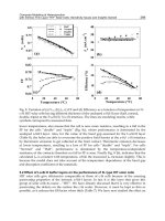
Fig. 22. Measured, simulated and calculated total transmitter energy dependence on the
value of misalignment.
© 2009 IEEE
© 2009 IEEE
Solid State Circuits Technologies
298
Measured results match well with both simulation results from electro-magnetic solver and
calculated results from (1). As mentioned in Sect. II, (1) does not cover all of region and has
an invalid region. The gap between measured and calculated results becomes larger as the
result curves approach the invalid region.
80
Normalized Required Total Transmitter Energy
Misalignment, ΔX [μm]
BER = 10
-10
, Timing Margin = 100ps
0
16 32
48
64
1
1.5
2
0.5
D
Δ
X
Tx Inductor
Rx Inductor
D=80μmD=80μm
D=160μmD=160μm
Simulated by EM SolverSimulated by EM Solver
Calculated by Equation (1)Calculated by Equation (1)
0
Communication Distance = 70μm
(Measured)
(Measured)
D=80μm
D=160μm
Fig. 23. Measured, simulated and calculated normalized total transmitter energy
dependence on the value of misalignment.
CLK
IBSC
CPU2
CPU0
CPU4CPU6
CPU3CPU1 CPU5CPU7
System
Bus
CLK
IBSC
CPU2
CPU0
CPU4CPU6
CPU3CPU1 CPU5CPU7
System
Bus
SRAM
65nm CMOS, 6.2mm * 6.2mm
Processor
90nm CMOS, 10.61mm * 9.88mm
L
o
w
e
r
C
h
i
p
Inductive-Coupling Link
(Data and Clock)
Inductive-Coupling Link
(Data and Clock)
Inductive-Coupling
Link
1MB-
SRAM
Memory
Controller
Inductive-Coupling
Link
1MB-
SRAM
Memory
Controller
U
p
p
e
r
C
h
i
p
U
p
p
e
r
C
h
i
p
Inductive-Coupling
Link
Wire Bonding
(Only Power Supply)
Fig. 24. Chip microphotograph and overhead view of stacked chips.
© 2009 IEEE
© 2009 IEEE
An Inductive-Coupling Inter-Chip Link for High-Performance and Low-Power 3D System Integration
299
5. Inductive-coupling link for processor-memory interface
5.1 Introduction
This section presents a three-dimensional (3D) system integration of a commercial processor
and a memory by using inductive coupling. A 90nm CMOS 8-core processor, back-grinded
to a thickness of 50μm, is mounted face down on a package by C4 bump. A 65nm CMOS
1MB SRAM of the same thickness is glued on it face up, and the power is provided by
conventional wire-bonding. The two chips under different supply voltages are AC-coupled
by inductive coupling that provides a 19.2Gb/s data link. Measured power and area
efficiency of the link is 1pJ/b and 0.15mm
2
/Gbps, which is 1/30 and 1/3 in comparison
with the conventional DDR2 interface respectively (Ito et al., 2008). The power efficiency is
improved by narrowing a transmission data pulse to 180ps. Reduced timing margin for
sampling the narrow pulse, on the other hand, is compensated against timing skews due to
layout and PVT variation by a proposed 2-step timing adjustment using an SRAM through
mode. All the bits of the SRAM is successfully accessed with no bit error under changes of
supply voltages (±5%) and temperature (25°C, 55°C).
5.2 Performance summary of developed 3D LSI system
Micrographs of the chips and their stacking are presented in Fig. 24. A 90nm CMOS
processor is mounted face down on a package by C4 bump. A 65nm CMOS SRAM is glued
on it face up, and the power is provided by conventional wire-bonding.
Figure 25 summarizes performance. The two chips are each fabricated in their optimal
process and supplied with optimal voltages. Thickness of the chips is both 50μm. The radius
of the inductors is the same as the communication distance, 120μm. There are 18 data
channels for uplink and downlink each. In total 36 inductors are arranged in a 243μm by
320μm pitch. Both the rising and falling edges of a clock are used for 2 phase interleaving to
reduce crosstalk between the adjacent channels (Miura et al., 2007). There are clock channels
for source synchronous transmission (Miura et al., 2009). One size larger inductors are
employed to strengthen the coupling coefficient for asynchronous channel. Total layout area
for the inductive coupling link is 2.82mm
2
. Aggregated bandwidth is 19.2Gb/s. Area
normalized by bandwidth is 0.15mm
2
/Gbps, which is 1/3 of a conventional DDR2 interface
in the same technology (Ito et al., 2008). Since the previous designs of the processor and the
memory were reused in large part, the inductive coupling channels are placed in the
peripheral region. They can be distributed to each core if a chip layout is carried out from
scratch. The circuitry alone occupies an area of 0.072mm
2
, which is only 2.6% of the total
area for the inductive coupling link. The area efficiency of circuit alone is therefore
0.0038mm
2
/Gbps, which is 1/120 of the conventional DDR2 interface. Even if the inductor is
placed above a bit line of an SRAM and transmits data, no interference is observed (Niitsu et
al., 2007). The inductive coupling can be applied to DRAM as well. The inductor can be
constructed using 2 metal layers.
5.2 System architecture design with adaptive timing adjustment
Figure 26 depicts a block diagram of the developed 3D LSI system. An inductive-coupling
bus state controller (IBSC) supports packet-based communications by adding two signals
(vld and eop). A control register in IBSC is used for timing adjustment. The timing
Solid State Circuits Technologies
300
Channel Pitch
X: 243μm, Y: 320μm
Data and Clock Link
Inductive-Coupling
120μm (Glue:20μm)
Communication Distance
Inductor Size
Data : 240μm, Clock : 350μm
Process
90nm CMOS
65nm CMOS
Supply Voltage 1.0 V 1.2 V
Chip Processor SRAM
Stacking Face-Down Face-Up
Connection with PCB Area Bump Wire Bonding
Thickness
50 μm 50 μm
(High Speed)(Property) (Low Power)
Total Bandwidth
19.2 Gbps
1pJ/b (1/30 of DDR2)
Energy Efficiency
Area Efficiency
0.15mm
2
/Gbps (1/3 of DDR2)
Channel Pitch
X: 243μm, Y: 320μm
Data and Clock Link
Inductive-Coupling
120μm (Glue:20μm)
Communication Distance
Inductor Size
Data : 240μm, Clock : 350μm
Channel Pitch
X: 243μm, Y: 320μm
Channel Pitch
X: 243μm, Y: 320μm
Data and Clock Link
Inductive-Coupling
Data and Clock Link
Inductive-Coupling
120μm (Glue:20μm)
Communication Distance
120μm (Glue:20μm)
Communication Distance
Inductor Size
Data : 240μm, Clock : 350μm
Inductor Size
Data : 240μm, Clock : 350μm
Process
90nm CMOS
65nm CMOS
Supply Voltage 1.0 V 1.2 V
Chip Processor SRAM
Stacking Face-Down Face-Up
Connection with PCB Area Bump Wire Bonding
Thickness
50 μm 50 μm
(High Speed)(Property) (Low Power)
Process
90nm CMOS
65nm CMOSProcess
90nm CMOS
65nm CMOS
Supply Voltage 1.0 V 1.2 VSupply Voltage 1.0 V 1.2 V
Chip Processor SRAMChip Processor SRAM
Stacking Face-Down Face-UpStacking Face-Down Face-Up
Connection with PCB Area Bump Wire BondingConnection with PCB Area Bump Wire Bonding
Thickness
50 μm 50 μm
Thickness
50 μm 50 μm
(High Speed)(Property) (Low Power)(High Speed)(Property) (Low Power)
Total Bandwidth
19.2 Gbps
1pJ/b (1/30 of DDR2)
Energy Efficiency
Area Efficiency
0.15mm
2
/Gbps (1/3 of DDR2)
Total Bandwidth
19.2 Gbps
Total Bandwidth
19.2 Gbps
1pJ/b (1/30 of DDR2)
Energy Efficiency
1pJ/b (1/30 of DDR2)
Energy Efficiency
Area Efficiency
0.15mm
2
/Gbps (1/3 of DDR2)
Area Efficiency
0.15mm
2
/Gbps (1/3 of DDR2)
Fig. 25. Performance Summary.
System Bus
Core #0~ #7
1-MB SRAM Module (Working Memory for CPU)
8 Cores
Inductive-
Coupling
Data Link
19.2 Gbps
Clock
Controller
*IBSC
Inductive-
Coupling
Clock Link
600MHz
*IBSC : Inductive-Coupling
Bus State Controller
Ctrl. Register
PHY of Inductive-Coupling Link Timing Ctrl.
300MHz
300MHz
600MHz
600MHz
PHY of Inductive-Coupling Link
BIST
Processor
SRAM
clk
*vld
*eop
data(16)
Valid Data
*vld : Valid(Strobe), *eop : End of Packet
150Mbps * 64bit
16bit
Packed-Based Communication
Fig. 26. Block diagram.
© 2009 IEEE
© 2009 IEEE
An Inductive-Coupling Inter-Chip Link for High-Performance and Low-Power 3D System Integration
301
adjustment is essential for a practical application. There is a trade off between power
dissipation and timing margin. Since power dissipation in a transmitter is in proportion to
the square of the pulse width (Miura et al., 2008), the narrower the pulse, the smaller the
power dissipation. The timing margin for sampling the narrow pulse, however, will be
reduced. Low-power design requires accurate timing control.
Adaptive circuits and systems are required to adjust the timing for the following reasons: 1)
timing jitter caused by PVT variations, especially in a clock path with long latency through
another chip, 2) VDD changes by DVS, and 3) inter-channel skews, especially when the
channels are distributed in a wide area. The timing jitter under PVT variations can be
monitored and calibrated by a coarse timing control unit with the control register in IBSC
(Fig. 27). Once the calibration result under each condition of DVS is stored in the control
register, the timing control unit can adjust the timing for DVS instantly by digital control.
DQ
600MHz Clk
QD
Rx
Tx
Rx
Tx
Tx
Rx
SRAM
Processor
Rx
Tx
QD
Coarse Timing
Control, T
D
Clk Tree
IBSC
Ctrl. Register
DQ
Coarse Timing
Control, T
U
Clk Tree
Fine Timing
Control
Fine Timing
Control
Clk ch. (1ch)
Clk ch. (1ch)
Data ch. (18ch)
Data ch. (18ch)
Downlink
Uplink
1-MB SRAM
Through
Mode
BIST
Controlled
by IBSC
DQDQ
600MHz Clk
QDQD
Rx
Tx
Rx
Tx
Tx
Rx
SRAM
Processor
Rx
Tx
QDQD
Coarse Timing
Control, T
D
Clk Tree
IBSC
Ctrl. Register
DQDQ
Coarse Timing
Control, T
U
Clk Tree
Fine Timing
Control
Fine Timing
Control
Fine Timing
Control
Fine Timing
Control
Clk ch. (1ch)
Clk ch. (1ch)
Data ch. (18ch)
Data ch. (18ch)
DownlinkDownlink
UplinkUplink
1-MB SRAM1-MB SRAM
Through
Mode
BISTBIST
Controlled
by IBSC
Fig. 27. Adaptive timing adjustment.
The inter-channel de-skew can be performed by a fine timing control unit that is
implemented in each channel. Figure 28 shows the timing adjustment flow that is controlled
by the processor. First, the control register sets a loopback path in the SRAM for a test mode
(an SRAM through mode). Secondly, pass/fail information, much like a shmoo plot, is
stored in a register for both the uplink and downlink by changing the coarse timing.
Thirdly, the coarse timing is set such that the timing margin becomes the largest when all
the channels pass. For each channel, fine timing is tuned next such that the timing margin
becomes the largest.
© 2009 IEEE
Solid State Circuits Technologies
302
SRAM
Processor
Timing in Uplink, T
U
Timing in Downlink, T
D
Timing in Uplink, T
U
Timing in Downlink, T
D
Coarse: Adjust
Fine: Fix
Coarse: Fix
Fine: Adjust
All ch.
Pass
(Shaded)
Tx
Rx
Tx
Rx
Optim.
Timing
Tx
Rx
Tx
Rx
16ch.
1) Coarse Timing Adjustment
2) Fine Timing Adjustment
Coarse
Fine
Fine
Clk
BIST
Coarse
Fine
Fine
Clk
Timing in
Downlink, T
D
Timing in
Uplink, T
U
Uplink Downlink
Through
Mode
SRAM
Processor
Timing in Uplink, T
U
Timing in Downlink, T
D
Timing in Uplink, T
U
Timing in Downlink, T
D
Coarse: Adjust
Fine: Fix
Coarse: Fix
Fine: Adjust
All ch.
Pass
(Shaded)
Tx
Rx
Tx
Rx
Optim.
Timing
Tx
Rx
Tx
Rx
16ch.
1) Coarse Timing Adjustment
2) Fine Timing Adjustment
CoarseCoarse
FineFine
FineFine
Clk
BIST
Coarse
Fine
Fine
Clk
Timing in
Downlink, T
D
Timing in
Uplink, T
U
Uplink Downlink
Through
Mode
Fig. 28. Fine and coarse (2-step) timing adjustment.
5.4 Measurement results and discussions
The SRAM was accessed (read and write) from the processor and BER was measured by
changing the control register. A timing shmoo plot is depicted in Fig. 29, a bathtub curve
marked by a broken line is also depicted. A BER of lower than 10
-14
is achieved with a 2
31
-1
PRBS. After optimizing the timing by setting the control register at the center of the shmoo
plot, tolerance against VDD and temperature changes was measured. The measured result is
presented in Fig. 30. No single bit failed under ±5% VDD variations and temperature
ranges from 25°C to 55°C. The VDD tolerance can be improved from ±5% to ±10%
by widening the pulse width from 180ps to 320ps at a cost of an increase in power efficiency
from 1pJ/b to 2.5pJ/b (still 1/12 of DDR2).
6. Conclusion
This chapter presents the fundamental investigation and application of an inductive-
coupling link.
First, the interference from power/signal lines and to SRAM of an inductive-coupling link
was investigated. Measurement result shows that influence from line and space (I) is none
and required normalized transmit power is 1.10 (line and space, type II) and 1.27 (mesh
type) when metal density is 16%. The line and space type of power line is better for the
© 2009 IEEE
An Inductive-Coupling Inter-Chip Link for High-Performance and Low-Power 3D System Integration
303
180ps
10
-12
10
-14
10
-8
10
-10
10
-4
10
-6
10
0
10
-2
Timing in Uplink, T
U
(36ps/step)
Bit Error Rate
Timing in Uplink, T
U
Timing in Downlink, T
D
16ch. Test
Test Pattern : PRBS 2
31
-1
After Fine Timing Adjustment
180ps
36ps/step
Optim. Timing
180ps
10
-12
10
-14
10
-8
10
-10
10
-4
10
-6
10
0
10
-2
Timing in Uplink, T
U
(36ps/step)
Bit Error Rate
Timing in Uplink, T
U
Timing in Downlink, T
D
16ch. Test
Test Pattern : PRBS 2
31
-1
After Fine Timing Adjustment
180ps
36ps/step
Optim. Timing
16ch. Test
Test Pattern : PRBS 2
31
-1
After Fine Timing Adjustment
180ps
36ps/step
Optim. Timing
Fig. 29. Measured bit error rate.
Variation in Supply Voltage of Processor Chip
0%
+
0%
+
+
+2.5% +5%2.5%2.5%5%5%
0%
+
0%
+
2.5%
5%
+2.5%
+5%
1.2V
1.05V
T=25 ℃
T=55 ℃
Achieved BER =10
-12
Test Pattern : PRBS 2
31
-1
5%
+
Variation in Supply Voltage5%
+
5%
+
+
Variation in Supply Voltage
PASS
Variation in Supply Voltage of SRAM Chip
FAIL
Fig. 30. Measured tolerance (BER<10
-12
) to variations in supply voltages and temperature.
© 2009 IEEE
© 2009 IEEE
Solid State Circuits Technologies
304
inductive-coupling link than mesh type. Additional power dissipation to achieve BER of 10
-8
is only 9% when signal line drives interconnect of 3mm length. In typical ranges, SRAM
array operation does not depend on existence of the inductive-coupling link.
Second, modeling of misalignment tolerance in inductive-coupling inter-chip link is
introduced. By comparing the calculated result based on the proposed modeling with the
measured result, the modeling was found to be accurate in common cases. The estimated
and measured results show that misalignment tolerance of inductive-coupling inter-chip
link is high enough to keep the performance under the existence of misalignment in usual
condition.
Third, application of an inductive-coupling link to interconnection of commercial MPU and
SRAM was performed. By exploiting proposed 2-step adaptive timing adjustment, reliable
operation under PVT variation has become possible. Achieved performances are power
efficiency of 1pJ/bit and area efficiency of 0.15mm
2
/Gbps, which are 1/30 and 1/3 of
conventional DDR2 interface, respectively.
7. Acknowledgements
This work has been in part supported by the Grant-in-Aid for JSPS fellows and the Central
Research Laboratory of Hitachi Limited.
8. References
Finkenzeller, K. (2003). RFID Handbook, Wiley, 2nd ed., 2003, pp 68-71
Fazzi, A., Canegallo, R., Ciccarelli, L., Magagni, L., Natali, F., Jung, E., Rolandi, P. &
Guerrieri, R. (2008). 3-D Capacitive Interconnections With Mono- and Bi-
Directional Capabilities, IEEE Journal of Solid-State Circuits, Vol. 43, No. 1, pp. 275-
284
Hattori, T., lrita, T., Ito, M., Yamamoto, E., Kato, H., Sado, G., Yamada, Y., Nishiyama, K.,
Yagi, H., Koike, T., Tsuchihashi, Y., Higashida, M., Asano, H., Hayashibara, I.,
Tatezawa, K., Shimazaki, Y., Morino, N., Hirose, K., Tamaki, S., Yoshioka, S.,
Tsuchihashi, R., Arai, N., Akiyama, T. & Ohno, K. (2006). A Power Management
Scheme Controlling 20 Power Domains for Single-Chip Mobile Processor,
Proceedings of IEEE International Solid-State Circuits Conference, pp. 2210-2219, Feb.,
2006
Ito, M., Hattori, T., Irita, T., Tatezawa, K., Tanaka, F., Hirose, K., Yoshioka, S., Ohno, K.,
Tsuchihashi, R., Sakata, M., Yamamoto, M. & Aral, Y. (2007). A 390MHz Single-
Chip Application and Dual-Mode Baseband Processor in 90nm Triple-Vt CMOS,
Proceedings of IEEE International Solid-State Circuits Conference, pp. 274-275, Feb.,
2007
Ito, M., Hattori, T., Yoshida, Y., Hayase, K., Hayashi, T., Nishii, O., Yasu, Y., Hasegawa, A.,
Takada, M., Mizuno, H., Uchiyama, K., Odaka, T., Shirako, J., Mase, M., Kimura, K.
& Kasahara, H. (2008). An 8640 MIPS SoC with Independent Power-Off Control of
8 CPUs and 8 RAMs by An Automatic Parallelizing Compiler, Proceedings of IEEE
International Solid-State Circuits Conference, pp. 90-91, Feb., 2008
An Inductive-Coupling Inter-Chip Link for High-Performance and Low-Power 3D System Integration
305
Koyanagi, M., Fukushima, T. & Tanaka, T. (2009). High-Density Through Silicon Vias for 3-
D LSIs, Proceedings of the IEEE, Vol. 97, No. 1, pp. 49-59
Matsumoto, T., Satoh, M., Sakuma, K., Kurino, H., Miyakawa, N., Itani, H. & Koyanagi, M.
(1998). New Three-Dimensional Wafer Bonding Technology Using the Adhesive
Injection Method, Japanese J. of Applied Physics, Vol. 37, No. 3B, pp. 1217-1221, Mar.
1998.
Miura, N., Mizoguchi, Sakurai, T. & Kuroda, T. (2004). Cross Talk in Inductive Inter-Chip
Wireless Superconnect, Proceedings of IEEE Custom Integrated Circuits Conference, pp.
99-102, Sept., 2004
Miura, N., Mizoguchi, D., Inoue, M., Niitsu, K., Nakagawa, Y., Tago, M., Fukaishi, M.,
Sakurai, T. & Kuroda, T. (2007). A 1 Tb/s 3 W Inductive-Coupling Transceiver for
3D-Stacked Inter-Chip Clock and Data Link, IEEE Journal of Solid-State Circuits, Vol.
42, No. 1, pp. 111-122
Miura, N., Ishikuro, H., Niitsu, K., Sakurai, T. & Kuroda, T. (2008). A 0.14pJ/bit Inductive-
Coupling Transceiver with Digitally-Controlled Precise Pulse Shaping, IEEE Journal
of Solid-State Circuits, Vol. 43, No. 1, pp. 285-291
Miura, N., Kohama, Y., Sugimori, Y., Ishikuro, H., Sakurai, T. & Kuroda, T. (2009). A High-
Speed Inductive-Coupling Link With Burst Transmission, IEEE Journal of Solid-State
Circuits, Vol. 44, No. 3, pp. 947-955
Mizoguchi, D., Miura, N., Ishikuro, H. & Kuroda, T. (2008). Constant Magnetic Field Scaling
in Inductive-Coupling Data Link, IEICE Transactions on Electronics, vol. E91-C, no. 2,
pp. 200-205, Feb., 2008.
Niitsu, K., Sugimori, Y., Kohama, Y., Osada, K., Irie, N., Ishikuro, H. & Kuroda, T. (2007).,
Interference from Power/Signal Lines and to SRAM Circuits in 65nm CMOS
Inductive-Coupling Link, Proceedings of IEEE Asian Solid-State Circuits Conference,
pp. 131-134, Nov., 2007
Niitsu, K., Kawai, S., Miura, N., Ishikuro, H. & Kuroda, T. (2008). A 65 fJ/b inductive-
coupling inter-chip transceiver using charge recycling technique for power-aware
3D system integration, Proceedings of IEEE Asian Solid-State Circuits Conference, pp.
97-100, Nov., 2008
Niitsu, K., Shimazaki, Y., Sugimori, Y., Kohama, Y., Kasuga, K., Nonomura, I., Saen, M.,
Komatsu, S., Osada, K., Irie, N., Hattori, T., Hasegawa, A. & Kuroda, T. (2009). An
inductive-coupling link for 3D integration of a 90nm CMOS processor and a 65nm
CMOS SRAM, Proceedings of IEEE International Solid-State Circuits Conference, pp.
480-481, Feb., 2009
Niitsu, K., Kohama, Y., Sugimori, Y., Kasuga, K., Osada, K., Irie, N., Ishikuro, H. & Kuroda,
T. (2010)., Modeling and Experimental Verification of Misalignment Tolerance in
Inductive-Coupling Inter-Chip Link for Low-Power 3D System Integration, IEEE
Transactions on VLSI Systems, (in print)
Onizuka, K., Kawaguchi, H., Takamiya, M., Kuroda, T. & Sakurai, T. (2006). Chip-to-Chip
inductive wireless power transmission system for SiP applications, Proceedings of
IEEE Custom Integrated Circuits Conference, pp. 575-578, Sept., 2006
Solid State Circuits Technologies
306
Yamaoka, M., Osada, K., Tsuchiya, R., Horiuchi, M., Kimura, S. & Kawahara, T. (2004). Low
power SRAM menu for SOC application using Yin-Yang-feedback memory cell
technology, Proceedings of IEEE Symposium on VLSI Circuits, pp. 288-291, Jun., 2004
Yamaoka, M., Maeda, N., Shinozaki, Y., Shimazaki, Y., Nii, K., Shimada, S., Yanagisawa &
Kawahara, T. (2005). Low-power embedded SRAM modules with expanded
margins for writing, Proceedings of IEEE International Solid-State Circuits Conference,
pp. 480-481, Feb., 2005
16
Polycrystalline Silicon Piezoresistive
Nano Thin Film Technology
Xiaowei Liu
1
, Changzhi Shi
1
and Rongyan Chuai
2
1
Harbin Institute of Technology
2
Shenyang University of Technology
China
1. Introduction
The piezoresistive effect of semiconductor materials was discovered firstly in silicon and
germanium (Smith, 1954). Dissimilar to the piezoresistive effect of metal materials induced
from the change in geometric dimension, the piezoresistive phenomenon in silicon is due to
that mechanical stress influences the energy band structure, thereby varying the carrier
effective mass, the mobility and the conductivity (Herring, 1955). The gauge factor (GF) is
used to characterize the piezoresistive sensitivity and defined as the ratio of the relative
resistance change and the generated strain (nondimensional factor). Usually, the GF in
silicon is around 100 and changes with stress direction, crystal orientation, doping
concentration, etc. Recently, the giant piezoresistances were observed in silicon nanowires
(He & Yang, 2006; Rowe, 2008) and metal-silicon hybrid structures (Rowe, et al., 2008),
respectively. Although these homogeneous silicon based materials or structures possess
high piezoresistive sensitivity, there are still several issues influencing their sensor
applications, such as, p-n junction isolation, high temperature instability, high production
cost and complex fabrication technologies.
As another monatomic silicon material with unique microstructure, polycrystalline silicon
has been investigated since the 1960s. The discovery of its piezoresistive effect (Onuma &
Sekiya, 1974) built up a milestone that this material could be applied widely in field of
sensors and MEMS devices. Moreover, polycrystalline silicon could be grown on various
substrate materials by physical or chemical methods, which avoids p-n junction isolation
and promotes further its applications for piezoresistive devices (Jaffe, 1983; Luder, 1986;
Malhaire & Barbier, 2003). Among numerous preparation methods, the most popular
technology is chemical vapour deposition (CVD), which includes APCVD, LPCVD, PECVD,
etc. The PECVD method can deposit films on substrates at lower temperatures, but the
stability and uniformity of as-deposited films are not good, and the samples could contain a
large number of amorphous contents. Subsequently, the metal-induced lateral
crystallization (MILC) technique was presented (Wang, et al., 2001). By enlarging grain size
and improving crystallinity, the gauge factor of MILC polycrystalline silicon was increased
to be about 60. But the MILC polycrystalline silicon-based devices could suffer the
contamination from the metal catalyst layer (e.g. Ni, Al, etc.). Compared with the
aforementioned technologies, the LPCVD process is a mature and stable CVD method with
Solid State Circuits Technologies
308
advantages of good product uniformity, low cost, IC process compatibility, etc. Therefore,
the preparation method in this work is mainly based on LPCVD, while the magnetron
sputtering technology will be utilized as a reference result.
The experimental results reported by other researchers indicate that the gauge factor of
polycrystalline silicon thicker films (around 400nm in thickness generally) has a maximum
as the doping concentration is at the level of 10
19
cm
-3
and then degrades rapidly with the
further increase of doping concentration (Schubert, et al., 1987; French & Evens, 1989;
Gridchin, et al., 1995; Le Berre, et al., 1996). Moreover, the gauge factor of highly doped
polycrystalline silicon thicker films is only 20-25. It results in that the research works were
emphasized on the medium doped polycrystalline silicon thicker films. However, the lower
doping concentration brings the higher temperature coefficients of resistance and gauge
factor. This limits the working temperature range of polycrystalline silicon thicker film-
based sensors.
In our research work, when the film thickness is reduced to nanoscale and the doping
concentration is elevated to the level of 10
20
cm
-3
, the enhanced piezoresistance effect is
observed, and the temperature coefficients of resistance and gauge factor are reduced
further. These phenomena are different from the polycrystalline silicon thicker films and can
not be explained reasonably based on the existing piezoresistive theory. The unique
properties of polycrystalline silicon nano thin films (PSNFs) could be useful for the design
and fabrication of piezoresistive sensors with miniature volume, high sensitivity, good
temperature stability and low cost. In the following sections, the details of sample
fabrication, microstructure characterization, experimental method and measurement results
will be provided. In order to analyze the experimental results, the tunnelling piezoresistive
theory is established and predicts the experimental results with a good agreement.
2. Film preparation technologies
2.1 Low pressure chemical vapor deposition
Due to the aforementioned advantages, the low pressure chemical vapour deposition
(LPCVD) technology is utilized to prepare the polycrystalline silicon films. According to the
difference of technological parameters, three groups of film samples were prepared (Group
A — different thicknesses; Group B — different doping concentrations; Group C — different
deposition temperatures).
a. Group A — Firstly, by controlling deposition time, the polycrystalline silicon thin films
with different thicknesses were deposited on 500 μm-thick (100) and (111) silicon
substrates (4 inch diameter) coated with 1μm-thick thermally grown SiO
2
layers by
LPCVD at 620 °C at 45~55 Pa, respectively. For the (100) substrates, the thicknesses of
as-deposited films are in the range of 30~90 nm; for the (111) substrates, the film
thicknesses are ranged from 123 nm to 251 nm. Then, the solid-state boron diffusion
was performed at 1080 °C in N
2
atmosphere with a flow rate of 2L/min to obtain the
doping concentration of 2.3×10
20
cm
-3
.
b. Group B — Subsequently, according to the piezoresistive sensitivities of polysilicon thin
films with different thicknesses, the optimal film thickness was extracted. The
experimental results show that the ~80 nm-thick films possess the highest gauge factor
(discussed later). Therefore, the thickness of polysilicon thin films with different doping
concentrations was selected to be 80 nm. After the same LPCVD process, the obtained
polysilicon thin films were ion-implanted by boron dopants with doses of
Polycrystalline Silicon Piezoresistive Nano Thin Film Technology
309
9.4×10
13
~8.2×10
15
cm
-2
. Then, the post-implantation annealings were carried out in N
2
at
1080 °C for 30 min to activate dopants and eliminate ion-implantation damages. Finally,
the doping concentrations were in the range of 8.1×10
18
~ 7.1×10
20
cm
-3
.
c. Group C — Before preparing films, a 1 μm-thick SiO
2
layer was grown on the 500 μm-
thick (111) Si wafers (4 inch diameter) by thermal oxidization at 1100 °C. Then, the 80
nm-thick PSNFs were deposited on the thermally oxidized Si substrates by LPCVD at a
pressure of 45~55 Pa over a temperature range of 560~670 °C. The reactant gas was SiH
4
and the flow rate was 50 mL/min. Since the films deposited at 560~600 °C exhibited
amorphous appearance mixed with polycrystals, the pre-annealing was performed on
them in dry N
2
at 950° C for 30 min to induce the recrystallization of amorphous
regions. For the dopant implantation, boron ions were implanted into the samples at a
dose of 2×10
15
cm
-2
at 20 keV. For the sake of dopant activation and ion implantation
damage elimination, the post-implantation annealing was carried out in N
2
atmosphere
at 1080 °C for 30 min. Then, the doping concentration was estimated to be 2×10
20
cm
-3
.
2.2 Magnetron sputtering
As a reference, a group of samples were prepared by magnetron sputtering. Before
preparing films, a 1 μm-thick SiO
2
layer was grown on the 500 μm-thick (100) Si wafers (4
inch diameter) by thermal oxidization at 1100 °C. Then, the polycrystalline silicon films were
prepared by magnetron sputtering system from an undoped silicon target and the substrate
temperature was 300 °C. The base pressure of system was maintained at 0.12 Pa. The
discharge current on the magnetron was held constant at 0.3 A, while the substrate bias
voltage was 500 V. The sputtering time was 10 min, and the thickness of films was 200 nm.
Through the SEM observation, it can be seen that the obtained films are amorphous. Thus,
the annealing of 1080 °C was carried out in N
2
atmosphere for 60 min to obtain the lowest
film resistivity. After annealing, the solid-state boron diffusion was performed at 1080 °C in
N
2
with a flow rate of 2 L/min to obtain the doping concentration of 2.3×10
20
cm
-3
.
3. Microstructure characterization
3.1 Samples with different thicknesses
In order to analyze the surface morphology, the film samples with different thicknesses
were characterized by SEM. The SEM images of samples with different thicknesses are given
in Fig. 1. For the characterization of grain orientation, the XRD experiment was performed.
The XRD patterns of samples with different thicknesses are shown in Fig. 2. From the SEM
images in Fig. 1, it can be seen that the grain size of the samples increases with increasing
film thickness. For 30, 40, 60, 90, 123, 150, 198, 251 nm-thick samples, their grain sizes are 11,
30, 37, 48, 48, 58, 69, 80 nm, respectively. By XRD analysis, the (111) peaks of the films
thicker than 120 nm and the (400) peaks of the films thinner than 100 nm are attributed to
the crystal orientation of substrates. It can be also observed that the (220), (400) and (331)
peaks appear as the films are thicker than 120 nm and the intensities of these diffract peaks
increase with the increase of film thickness. Moreover, the (311) peak is observed in 251 nm-
thick films. It indicates that the increase in film thickness improves the crystallinity and
enhances the preferred growth. However, no obvious diffract peaks are observed in 60 and
90 nm-thick films, so they could be considered to be randomly oriented. Noticeably, the
(201) peaks appear in 30 and 40 nm-thick samples. According to the report (Zhao et al.,
2004), this preferred orientation occurs in nanocrystalline silicon and corresponds to
Solid State Circuits Technologies
310
tetragon microstructure. It indicates that these two samples exhibit the structural
characteristic of nanocrystalline silicon. For the sake of brevity, the 60-100 nm-thick films are
called polysilicon nano thin films (PSNFs), while the films thicker than 120 nm are called
polysilicon common films (PSCFs). The films thinner than 50 nm are called nanocrystalline-
like polysilicon thin films (NL-PSTFs).
Fig. 1. SEM images of polycrystalline silicon thin film samples with different thicknesses
Fig. 2. XRD patterns of polycrystalline silicon thin films with different thicknesses
3.2 Samples with different doping concentrations
Fig. 3 provides the SEM and TEM images of the 80 nm-thick PSNFs with doping
concentrations of 2×10
19
cm
-3
, 4.1×10
19
cm
-3
and 4.1×10
20
cm
-3
. It can be observed that the
variation of doping concentration does not influence the grain size obviously. Thus, the
grain size of the samples with different doping concentrations is considered to be constant.
In the XRD pattern of Fig. 4, only the weak (220) peak is observed and the strong (111) peak
is attributed to the crystal orientation of substrates. It indicates that these samples are
randomly oriented.
Polycrystalline Silicon Piezoresistive Nano Thin Film Technology
311
Fig. 3. TEM and SEM images of 80 nm-thick PSNF samples with different doping
concentrations. (a) 2×10
19
cm
-3
TEM; (b) 4.1×10
19
cm
-3
SEM; (c) 4.1×10
20
cm
-3
SEM
Fig. 4. XRD spectrum of 80 nm-thick polycrystalline silicon nano thin films
3.3 Samples with different deposition temperatures
The surface morphology of PSNFs was characterized by SEM, as shown in Figs. 5(a)-(e). It
can be seen that the grain size increases with elevating deposition temperature. This
indicates that the crystallinity of PSNFs can be improved by raising deposition temperature.
The grain size can be determined by TEM, as shown in Fig. 5(f). The mean grain size of
620 °C samples is estimated to be 40 nm approximately. With the deposition temperature
varying from 560 °C to 670 °C, the mean grain size increases from 30 nm to 70 nm. For the
sake of clarity, the 560~600 °C films undergoing the preannealing of 950 °C are called
Fig. 5. SEM and TEM images of PSNFs deposited at different temperatures
Solid State Circuits Technologies
312
recrystallized (RC) PSNFs, while the 620~670 °C films are called directly crystallized (DC)
PSNFs. From Fig. 5, it can be seen that the borders between grain boundaries and grains of
RC PSNFs are obscure as well as the 670 °C samples. It shows that the grain boundaries of
the abovementioned samples contain a large number of amorphous phases.
In order to analyze the film microstructure, the XRD experiment was performed on the
samples. In the XRD spectra shown in Fig. 6, all the (111) peaks are attributed to Si
substrates. The clear (220) peak of 670 °C PSNFs is due to the preferred grain growth along
(220) orientation, while the other PSNFs are oriented randomly. Furthermore, it should be
noted that the broad peaks (2θ=85~100 °) related to amorphous phases appear on the spectra
of RC and 670 °C PSNFs, thereby testifying the existence of amorphous phases at grain
boundaries. Because amorphous phases in the 620 °C PSNFs are much fewer, no remarkable
broad peak is observed. The peak intensity and FWHM of RC PSNFs are larger than those of
the 670 °C ones. It demonstrates that the crystallinity of RC PSNFs is lower than DC ones.
The broad peak of 670 °C samples is likely due to the preferred growth aggravating
disordered states of grain boundaries.
Fig. 6. XRD spectra of PSNF samples deposited at different temperatures
3.4 Magnetron sputtering samples
Fig. 7 provides the SEM images of polycrystalline silicon films prepared by magnetron
sputtering before and after the annealing of 1080 °C. From Fig. 7(a), we can see that the film
is amorphous and has no micrograined texture. After high temperature annealing, the
Fig. 7. SEM images of polycrystalline silicon films prepared by magnetron sputtering
Polycrystalline Silicon Piezoresistive Nano Thin Film Technology
313
recrystallization occurs in the film, which make the film transfer from amorphous state to
polycrystalline state, as shown in Fig. 7(b). By calculation, the grain size of magnetron
sputtering films is around 10 nm. It indicates that the crystallinity of magnetron sputtering
films is very low and the recrystallization induced by high temperature annealing is limited
for the improvement of film crystallinity.
4. Fabrication of cantilever beam samples
4.1 Piezoresistors
For measuring gauge factor, the cantilever beams were fabricated based on
photolithography and etching technologies. Firstly, the sample wafers were ultrasonically
degreased with methylbenzene, acetone and ethanol for 5 min in each and then rinsed
repeatedly in de-ionized water. The cleaned samples were pre-baked at 120 °C for 15 min.
Next, after spin-coating with positive photoresist and a soft-bake at 90°C for 10 min, the
samples were exposed for 90 s using the mask plate as shown in Fig. 8(a) and developed in
the 0.5% NaOH solution. Then, a hard-bake for 25 min was performed at 120 °C for the
successive etching process. After photolithography, the samples were etched in
HNO
3
/HAc/HF (4:1:1) solution to form PSNF resistors and then rinsed in de-ionized water.
The photoresist was removed by acetone to obtain the sample wafers with PSNF resistors as
shown in Fig. 8(b).
Fig. 8. Schematic diagram of mask plates and sample wafers in the fabrication of cantilever
beams. (a) The mask plate for patterning resistors. (b) The sample wafer after patterning
resistors. (c) The mask plate for patterning electrodes and calibrated scales. (d) The sample
wafer and the cantilever beam after fabricating electrodes and calibrated scales.
4.2 Metal contact electrodes
Here, the aluminium is used as the metal electrode material. In order to measure the contact
resistance between PSNFs and metal electrodes, the ohmic contact test patterns based on
linear transmission line model (LTLM) were also fabricated on the samples. Before
depositing metal, the samples were dipped in HF/H
2
O (1:10) for 8 s to remove the native
Solid State Circuits Technologies
314
oxide. The Al layer was evaporated onto the samples by vacuum evaporation. Then, the
positive photoresist was coated and patterned in the same process as the resistor fabrication.
The schematic diagram of mask plate is shown in Fig. 8(c). The Al layer was etched in
concentrated phosphorous acid at 80~100 °C to form electrodes. The electrode fabrication
was completed by removing the photoresist left.
4.3 Alloying and scribing
After scribing, the sample wafers were divided into individual cantilever beams of 26 mm×4
mm, as shown in Fig. 8(d). Then, the samples were alloyed at 410 °C, 450 °C and 490 °C for
20 min in N
2
to form ohmic contact. By measuring the LTLM test patterns, the I-V
characteristic curves after alloying at different temperatures are provided in Fig. 9. From
Fig. 9, it can be seen that the samples annealed at 450 °C have a linear I-V curve, which
indicates that the good ohmic contact is formed. The specific contact resistivity is about
2.4×10
-3
Ω·cm
2
.
Fig. 9. I-V characteristic curves of metal contact electrodes after annealed at different
alloying temperatures
Finally, on the actual cantilever beam sample given in Fig. 10, two groups of PSNF
piezoresistors were fabricated. Each group consists of three sets of longitudinal and
transversal piezoresistors with length-width ratios of 1:4, 2:1 and 8:1, respectively. And the
current directions through longitudinal resistors were aligned with the (110) orientation.
Fig. 10(b) and (c) are the micrographs of a PSNF resistor taken by laser scanning microscope.
Also, the Al calibrated scales were fabricated near both ends of cantilever beams for
measuring the arm of applied force.
5. Gauge factor measurement
The gauge factor test setup is shown in Fig. 11. Either end of the cantilever beam is fixed by the
clamp. The piezoresistors are connected to the electric instruments through Al electrodes.
Polycrystalline Silicon Piezoresistive Nano Thin Film Technology
315
Fig. 10. (a) Photo of a cantilever beam sample; (b) Laser scanning microscope 2D image of a
polysilicon piezoresistor; (c) Laser scanning microscope 3D image of a polysilicon
piezoresistor
Fig. 11. Strain loading setup for measuring gauge factor
When an axial force F is applied to the free end of the cantilever beam, the strain ε(x)
produced at x can be expressed as
2
6( )
()
lxF
x
bt Y
ε
−
⋅
=
(1)
where l is the force arm of the axial force F, b and t are the width and the thickness of the
cantilever beam (b, t << l here), respectively. Y is Young’s modulus of silicon. The initial
resistance R
0
(without strain) and the varied resistance R (with strain) were measured by a
Keithley 2000 digital multimeter. The gauge factor can be calculated by:
0
00
RR R
GF
RR
ε
ε
−Δ
==
⋅
⋅
(2)