Adaptive Techniques for Dynamic Processor Optimization Theory and Practice by Alice Wang and Samuel Naffziger_6 pdf
Bạn đang xem bản rút gọn của tài liệu. Xem và tải ngay bản đầy đủ của tài liệu tại đây (1.52 MB, 19 trang )
Chapter 4 Dynamic Adaptation Using Body Bias, Supply Voltage, and Frequency 83
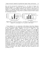
dies can be recovered by reducing the V
CC
. As shown in Figure 4.8,
applying adaptive V
CC
improves the mean die frequency as well as the
number of parts in the highest frequency bin. However, effectiveness of
adaptive V
CC
depends critically on the voltage resolution provided by the
voltage regulator module. Using 50mV resolution instead of 20mV renders
the technique ineffective.
0%
20%
40%
60%
80%
0.85 0.90 0.95 1.00 1.05
Frequency bin (normalized)
Accepted die count
Fixed Vcc: 1.05V
Adaptive Vcc (50mV
resolution)
Adaptive Vcc (20mV
resolution
)
0%
10%
20%
30%
40%
50%
-9% -7% -4% -2% 0% 2% 4%
Vcc (normalized)
Accepted die count
p
Nominal Vcc: 1.05V
Adaptive Vcc
Ada
p
tive Vcc+Vbs
Figure 4.8 (a) Comparison of fixed V
CC
and adaptive V
CC
, (b) Comparison of
adaptive V
CC
and adaptive V
CC
+V
BS
[8]. (© 2003 IEEE)
Using adaptive V
CC
in conjunction with adaptive body bias (adaptive
V
BS
) is more effective than using either of them individually (Figure 4.8b).
In this combined scheme (adaptive V
CC
+V
BS
), a single V
CC
and
NMOS/PMOS V
BS
combination is used per die to move it to the highest
frequency bin subject to the active power limit. Adaptive V
BS
uses FBB to
speed up dies that are too slow, and RBB to reduce frequency and leakage
power of dies that are too fast and leaky. Adaptive V
CC
+V
BS
, on the other
hand, recovers these dies above the active power limit by (1) first lowering
V
CC
and natural operating frequency together to bring the sum total of their
switching and leakage powers well below the active power limit and (2)
then applying FBB to speed them up and move them to the highest
frequency bin allowed by the active power limit. As a result, more dies use
lower V
CC
values than adaptive V
CC
. In addition, more dies use FBB,
instead of RBB, compared to adaptive V
BS
(Figure 4.9). Since the
effectiveness of RBB for leakage power reduction diminishes with
technology scaling [4], adaptive V
CC
+V
BS
will be more effective in future
technology generations than adaptive V
BS
alone. Bias voltages for NMOS
and PMOS transistors are typically generated using on-die circuitry and
routed to transistor wells using a separate bias grid, incurring an area
overhead of 2–4%.
84 James Tschanz
2% 25%
Die count:
-0.4
-0.3
-0.2
-0.1
0
0.1
0.2
0.3
0.4
PMOS body bias (V
)
P FBB
N
RBB
P FBB
N FBB
P RBB
N
RBB
P RBB
N FBB
(a) Adaptive Vbs
2% 25%
Die count:
-0.4
-0.3
-0.2
-0.1
0
0.1
0.2
0.3
0.4
PMOS body bias (V
)
P FBB
N
RBB
P FBB
N FBB
P RBB
N
RBB
P RBB
N FBB
(a) Adaptive Vbs
-0.4
-0.3
-0.2
-0.1
0
0.1
0.2
0.3
0.4
-0.4 -0.3 -0.2 -0.1 0 0.1 0.2 0.3 0.4
NMOS body bias (V)
PMOS body bias (V
)
P FBB
N
RBB
P FBB
N FBB
P RBB
N
RBB
P RBB
N FBB
(b) Adaptive Vcc+Vbs
-0.4
-0.3
-0.2
-0.1
0
0.1
0.2
0.3
0.4
-0.4 -0.3 -0.2 -0.1 0 0.1 0.2 0.3 0.4
NMOS body bias (V)
PMOS body bias (V
)
P FBB
N
RBB
P FBB
N FBB
P RBB
N
RBB
P RBB
N FBB
(b) Adaptive Vcc+Vbs
-0.4 -0.3 -0.2 -0.1 0 0.1 0.2 0.3 0.4
NMOS body bias (V)
-0.4 -0.3 -0.2 -0.1 0 0.1 0.2 0.3 0.4
NMOS body bias (V)
Figure 4.9 Optimal body bias voltages chosen for (a) adaptive V
BS
, (b) adaptive
V
CC
+V
BS
[8]. (© 2003 IEEE)
4.3 Dynamic Variation Compensation
4.3.1 Dynamic Body Bias
Body bias can also be used in a dynamic sense as part of a power
management scheme or to compensate dynamic variations. Due to
advanced power control features, microprocessors can experience a very
wide range of activity factors during normal operation – ranging from very
high activity for tasks which are heavily computationally intensive to very
low activity when the processor is in standby mode. Therefore it is
impossible to find the device threshold voltage, supply voltage, and
frequency which is energy optimal across all usage conditions. Body bias
provides a way to adjust the threshold voltage dynamically to improve
performance during active mode while saving power in standby mode.
When the processor is actively running computations, the activity factor
is high, and typically dynamic power dominates over the leakage power. In
this case, forward body bias can be applied to lower the threshold voltage
and improve performance. Alternately, the device threshold voltage can be
increased in the process so that when FBB is applied, it is lowered to the
original target value. Applying FBB in this manner also has the advantage
of improving the short-channel effects of the devices compared to
lowering the V
T
through process only. When the processor goes into an
idle or standby mode, the power is dominated by transistor leakage. Zero
or reverse body bias can then be applied to raise the threshold voltage and
Chapter 4 Dynamic Adaptation Using Body Bias, Supply Voltage, and Frequency 85
reduce the leakage. In this manner, the processor operates much more
efficiently in both active and standby modes.
Scan
FIFO
Scan
out
Sleep
ALU
Body bias
Control
Figure 4.10 Dynamic ALU test-chip with on-chip PMOS body bias [9].
(© 2003 IEEE)
An implementation of dynamic body bias for power control is shown in
Figure 4.10. This test-chip in 130nm CMOS technology [9] includes a 32-
bit dynamic ALU with on-chip dynamic body bias for the PMOS
transistors. The body bias circuitry consists of two main blocks: a central
bias generator (CBG) and many distributed local bias generators (LBGs)
(Figure 4.11). The function of the CBG is to generate a process, voltage,
and temperature-invariant reference voltage which is then routed to the
local bias generators. The CBG uses a scaled bandgap circuit to generate a
reference voltage which is 450mV below the bandgap supply V
CCA
– this
represents the amount of forward bias to apply in active mode. This
reference voltage is then routed to all of the distributed local bias
generators, shielded on both sides by V
CCA
. The function of the LBG is to
translate this voltage, referenced to V
CCA
, to a body voltage which is
referenced to the local block V
CC
. This ensures that any variations in the
local V
CC
will be tracked by the body voltage, maintaining a constant
450mV of FBB. Translation of the reference is accomplished through the
use of a current mirror followed by a voltage buffer to drive the final n-
well load. Low-frequency tracking of supply variations is handled by the
current mirror while a capacitor provides the high-frequency tracking. In
idle mode, the current mirror is disabled and a zero-bias switch transistor
connects the body to V
CC
, applying zero body bias for leakage reduction. A
total of 40 distributed LBGs are used to bias the ALU, and the total area
overhead for this body bias technique is 6–8%, including the bias
generators as well as the additional routing required to separate the body
terminals from the supply.
86 James Tschanz
Vcca
Vcca - 450mV
(shielded)
Scaled
bandgap
Local Vcc - 450mV
Current
mirror
Local Bias Generators
Central Bias
Generator
Zero-bias
switch
Vcca
Vcca
Control
Vref
Figure 4.11 Bias generator circuits for dynamic ALU test-chip [9].
(© 2003 IEEE)
The adder operational frequency ranges from 3GHz (1.05V) to 4.2GHz
(1.4V) when zero body bias (ZBB) is applied to the PMOS transistors in
the core (Figure 4.12a). If the dynamic body bias circuitry is enabled to
apply 450mV FBB to the core, the frequency improves by 3–7%. To
achieve a target frequency of 4.05GHz, the supply voltage must be set to
1.35V when no body bias is used but can be lowered to 1.28V with FBB.
This supply voltage reduction results in lower switching power for the
FBB design at the same clock frequency. When the adder is put into
standby mode, ZBB is used for the core, and this results in a leakage
reduction of 2×. Total power savings for the ALU at a typical activity
profile are shown in Figure 4.12b – for this example, the dynamic bias
achieves 8% total power reduction. Therefore dynamic body biasing
allows the frequency improvement due to FBB coupled with the reduced
leakage power of ZBB.
0
2
4
6
8
10
12
Clock gating only Clock gating +
body bias
Tota power (mW)
1.28V 1.28V
Switching
Leakage
Overhead
8%
savings
↓
45%
LBG
only
0
2
4
6
8
10
12
Clock gating only Clock gating +
body bias
Tota power (mW)
1.28V 1.28V
Switching
Leakage
Overhead
8%
savings
↓
45%
LBG
only
2.5
3
3.5
4
4.5
1 1.1 1.2 1.3 1.4 1.5
Vcc (V)
Frequency (GHz)
ZBB
450mV FBB to core
4.05GHz
75 ° C, No sleep transistor
1.28V
1.35V
5% lower V
CC
for
same frequency
5% frequency
increase
2.5
3
3.5
4
4.5
1 1.1 1.2 1.3 1.4 1.5
Vcc (V)
Frequency (GHz)
ZBB
450mV FBB to core
4.05GHz
75 ° C, No sleep transistor
1.28V
1.35V
5% lower V
CC
for
same frequency
5% frequency
increase
Figure 4.12 (a) Maximum frequency vs. supply voltage for ALU with and
without body bias. (b) Typical power savings due to dynamic body bias [9].
(© 2003 IEEE)
Chapter 4 Dynamic Adaptation Using Body Bias, Supply Voltage, and Frequency 87
4.3.2 Dynamic Supply Voltage, Body Bias, and Frequency
While static techniques such as clock tuning, adaptive body bias, and
adaptive supply voltage can effectively compensate process variations,
other variations such as temperature, voltage droops, noise, and transistor
aging are dynamic and change throughout the lifetime of the processor.
These cannot be compensated using a static technique and are typically
guardbanded using either reduced frequency or higher supply voltage. This
guardbanding is expensive in terms of performance and power and is
becoming prohibitive as design margins shrink. To achieve an energy-
efficient microprocessor which operates correctly in the presence of these
variations, a method of sensing the environment and responding by
changing voltage, body bias, or frequency is necessary. In this section, we
describe one implementation of a dynamic adaptive processor design.
4.3.2.1 Design Details
The test-chip in 90nm CMOS technology (Figure 4.13) contains a TCP
offload accelerator core, a data input buffer, V
CC
droop sensors, thermal
sensors, a dynamic adaptive biasing (DAB) control unit, distributed noise
injectors, body bias generators, and a three-PLL dynamic clocking unit
[10]. The DAB controller receives inputs from the thermal sensors and
droop detectors. Average supply current is sensed by the off-chip voltage
regulator module (VRM), and digitally communicated to the DAB
controller on chip. The programmable noise injectors are used to generate
various supply noises and load currents, in addition to that generated by
Figure 4.13 Block diagram of the dynamic adaptive TCP/IP processor [10].
(© 2007 IEEE)
TCP/IP
processor
PLL0
PLL1
DAB
Control
Thermal
sensor
Div
PMOS
CBG
NMOS
CBG
core clk
gate
Droop
sensor
Time
Time
PLL2
NMOS body bias
PMOS body bias
I/O clk
Noise
injector
F
0
F
1
F
2
ctrl
VRM
(off-die)
88 James Tschanz
Figure 4.14 Organization of the dynamic adaptive bias controller, and the
interface to the dynamic clocking and body bias circuits [10]. (© 2007 IEEE)
Responding to the relatively fast V
CC
droops also requires a method for
changing frequency quickly without waiting for a PLL to relock. The
clocking subsystem, shown in Figure 4.15, contains three PLLs running at
independent frequencies and a multiplexer to select between them in a
single cycle while ensuring that there are no shortened clock cycles.
Several algorithms for changing frequency by switching between multiple
PLLs are implemented as part of the frequency control, including a simple
algorithm which switches between three locked PLLs, to a flexible
algorithm which keeps one PLL always locked at a frequency higher and
lower than the current frequency. When a frequency change is requested, a
the core during normal operation. The DAB controller drives the dynamic
frequency unit, body bias generators, and voltage setting of the off-chip
VRM to dynamically adapt frequency, body bias, and V
CC
to achieve opti-
mum settings for the given conditions. This DAB controller (Figure 4.14)
is based on a lookup table which is indexed by the output of the thermal,
droop, and current sensors and is loaded with pre-characterized data
representing the optimum V
CC
, body bias, and frequency for each of the
sensor combinations. The control also includes programmable timers and
logic to ensure that transitions in V
CC
, body bias, and frequency happen in
the correct sequence needed for fault-free operation and to eliminate
instability around the sensor trip points. The control is designed to be fast
enough to respond to 2nd and 3rd droops in voltage as well as changes in
temperature and overall chip activity factor.
Chapter 4 Dynamic Adaptation Using Body Bias, Supply Voltage, and Frequency 89
switch is made to the slower (or faster) PLL, and then the other two PLLs
are relocked and the process repeated. This allows the entire frequency
space to be covered in 3% steps. The dynamic frequency algorithms are
implemented in the DAB control, and commands are sent to the PLL block
to switch between PLLs and update PLL divider values. Clock gating is
also implemented to reduce active power consumption of the core when
the TCP/IP header has finished processing and the core is idle. Both
NMOS and PMOS body bias generators are implemented on the die and
each includes a central bias generator (CBG) which is controlled by the
DAB control, and many local bias generators (LBGs) distributed
throughout the die. The PMOS bias implementation includes a differential
difference amplifier (DDA) which allows both reverse and forward bias
values to be generated with 32mV resolution. The NMOS bias
implementation uses a simpler matched source-follower LBG for forward
body bias only. Input header data to the core is supplied from the on-chip
input buffer, and all arrays and programmable features are loaded through
JTAG scan.
Figure 4.15 Dynamic clocking circuitry using multiple PLLs for fast frequency
control [10]. (© 2007 IEEE)
4.3.2.2 Measurement Results
Maximum frequency of the design ranges from 2.2GHz at 1V to 3.4GHz at
1.4V, and total power consumption at 1.2V is 1.3W for a high-activity test.
Frequency can be increased by 9–22% through application of NMOS and
PMOS forward body bias. F
MAX
and power measurements are taken across
a range of voltages, body biases, and temperatures and the results loaded
into the DAB control lookup table. Dynamic response of the chip to
90 James Tschanz
temperature changes during a high-workload test (Figure 4.16) shows that
while the worst-case frequency is set by the highest expected temperature,
as the temperature drops, the core frequency can be increased. At the same
time, at low temperature, the leakage component of power is reduced, and
forward body bias (in this example, NMOS forward body bias) can be
applied to further increase the performance. This combination reduces the
guardband needed for maximum temperature and, in this example, results
in a 1.4% increase in average frequency over the duration of the test.
In a similar way, clock frequency can be adjusted in response to
dynamic voltage droops that occur due to step changes in current demand
by the processor (Figure 4.17). In this case, a sudden increase in current
demand causes a voltage droop to occur, after which the voltage settles to
a lower voltage determined by the IR drop of the power delivery network.
While a standard design would have to operate at a frequency determined
by the worst-case voltage during the droop, the adaptive processor can
detect the droop and dynamically respond by lowering frequency. The
maximum frequency can then by increased by 32% for this large voltage
droop, improving average performance for the workload.
0
20
40
60
80
100
Temperature (C)
2600
2700
2800
2900
3000
3100
0 1000 2000 3000
Time (ms)
Frequency (MHz
)
0
0.2
0.4
0.6
0.8
1
Body bias (V)
← Frequency
Body Bias →
0
20
40
60
80
100
Temperature (C)
2600
2700
2800
2900
3000
3100
0 1000 2000 3000
Time (ms)
Frequency (MHz
)
0
0.2
0.4
0.6
0.8
1
Body bias (V)
← Frequency
Body Bias →
Figure 4.16 Response of frequency and body bias to dynamic temperature change
[10]. (© 2007 IEEE)
Dynamic frequency and body bias capabilities also allow the design to
respond to frequency degradation that results from device-aging
mechanisms such as NBTI [11]. The threshold voltage increase in the
PMOS devices due to aging can be compensated by applying increasing
Chapter 4 Dynamic Adaptation Using Body Bias, Supply Voltage, and Frequency 91
0.4
0.6
0.8
1
1.2
1.4
Voltage (V)
0
500
1000
1500
2000
2500
3000
0 1020304050
Time (us)
Frequency (MHz)
Figure 4.17 Response of clock frequency to dynamic voltage droops [10].
(© 2007 IEEE)
amounts of PMOS forward body bias over the lifetime of the part.
Measurements (Figure 4.18) show that the maximum frequency of the part
degrades by ~3% over its lifetime, requiring an initial frequency
guardband of more than 3% due to process variations. By applying the
correct amount of PMOS body bias, the threshold voltage can be reduced
back to its initial value, counteracting the effects of aging and allowing the
part to remain at a constant frequency over its lifetime. This allows the
aging guardband to be removed and the performance of the part to be
increased.
0
20
40
60
80
100
120
0 50 100 150 200
Aging Time (Hours)
PMOS Body Bias (mV)
0.9V
1.2V
1500
1550
1600
1650
1700
Fmax (MHz)
Ag
ed Fmax
(
0.9V
)
Compensated Fmax
Figure 4.18 Aging compensation using dynamic body bias. The amount of FBB
required to completely compensate aging is similar for both 0.9V and 1.2V supply
[10]. (© 2007 IEEE)
92 James Tschanz
4.4 Conclusion
Both static variations such as process fluctuation and dynamic variations in
voltage, temperature, and aging are increasing with each technology
generation. Simply worst-casing these variations during the design phase is
no longer viable as this results in a design which is nonoptimal in power
and performance. These variations need to be handled using a combination
of variation-tolerant circuit techniques, architecture innovations, and
system-level dynamic response.
Body bias can be used for both static variation compensation during
active mode and leakage reduction for a low-power standby mode. Body
bias can also be used as a method of dynamic response – maintaining circuit
operation through a voltage droop for compensating transistor degradation
due to aging. In much the same way, supply voltage can be statically set to
compensate the die-to-die variations, or dynamically changed in response to
temperature and power fluctuations. Finally, clock frequency can be
modulated in a processor to adapt to the current environmental conditions.
These three techniques can be combined to handle both static and dynamic
variations in an efficient and low-overhead way.
References
[1] K. A. Bowman, S. G. Duvall, and J. D. Meindl, “Impact of die-to-die and
within-die parameter fluctuations on the maximum clock frequency
distribution for gigascale integration”, IEEE J. Solid-State Circuits, Vol. 37,
pp. 183–190, Feb. 2002.
[2] N. A. Kurd, J. S. Barkatullah, R. O. Dizon, T. D. Fletcher, and P. D. Madland,
“A multigigahertz clocking scheme for Pentium® 4 micro-processor”, IEEE
J. Solid-State Circuits, Vol. 36, pp. 1647–1653, Nov. 2001.
[3] A. Keshavarzi et al., “Technology scaling behavior of optimum reverse body
bias for standby leakage power reduction in CMOS IC’s”, Proc. ISLPED,
[4] A. Keshavarzi, S. Ma, S. Narendra, B. Bloechel, K. Mistry, T. Ghani,
S. Borkar, and V. De, “Effectiveness of reverse body bias for leakage control
in scaled dual V
T
CMOS ICs”, Proc. ISLPED, pp. 207–212, Aug. 2001.
[5] S. Narendra et al., “Forward body bias for microprocessors in 130nm
technology generation and beyond”, IEEE J. Solid-State Circuits, Vol. 38,
No. 5, May 2003.
[6] S. Narendra, M. Haycock, V. Govindarajulu, V. Erraguntla, H. Wilson,
S. Vangal, A. Pangal, E. Seligman, R. Nair, A. Keshavarzi, B. Bloechel,
G. Dermer, R. Mooney, N. Borkar, S. Borkar, and V. De, “1.1V 1GHz
communications router with on-chip body bias in 150nm CMOS”, IEEE
ISSCC Dig. Tech. Papers, pp. 270–271, Feb. 2002.
pp. 252–254, Aug. 1999.
Chapter 4 Dynamic Adaptation Using Body Bias, Supply Voltage, and Frequency 93
[7] J. Tschanz, J. Kao, S. Narendra, R. Nair, D. Antoniadis, A. Chandrakasan,
and V. De, “Adaptive body bias for reducing impacts of die-to-die and
within-die parameter variations on microprocessor frequency and leakage”,
IEEE J. Solid-State Circuits, Vol. 37, Issue 11, pp. 1396–1402, Nov. 2002.
[8] J. Tschanz et al., “Effectiveness of adaptive supply voltage and body bias for
reducing impact of parameter variations in low-power and high-performance
microprocessors”, IEEE J. Solid State Circuits, Vol. 38, No. 5, May 2003.
[9] J. Tschanz et al., “Dynamic sleep transistor and body bias for active leakage
power control of microprocessors”, IEEE J. Solid State Circuits, Vol. 38,
No. 11, Nov 2003.
[10] J. Tschanz et al., “Adaptive frequency and biasing techniques for tolerance to
dynamic temperature-voltage variations and aging”, IEEE ISSCC Dig. Tech.
Papers, Feb. 2007.
[11] D. Schroder et al., J. Appl. Phys., Vol. 94, No. 1, July 2003.
Chapter 5 Adaptive Supply Voltage Delivery
Yogesh K. Ramadass, Joyce Kwong, Naveen Verma, Anantha Chandrakasan
Massachusetts Institute of Technology
Minimizing the power consumption of battery-powered systems is a key
focus in integrated circuit design. The increased importance of power is
even more notable for a new class of energy-constrained systems. These
systems must achieve long system lifetimes from a limited energy source,
so the need to reduce energy consumption whenever possible is para-
mount. Dynamic voltage scaling (DVS) [1] is a popular method to achieve
energy efficiency in systems that have widely variant performance de-
mands. As V
DD
decreases, transistor drive currents decrease, bringing
down the speed of operation of a circuit. A DVS system adjusts the supply
voltage, operating the circuit at just enough voltage to meet performance,
thereby achieving overall savings in total power consumed.
Figure 5.1a plots the required rate of the system versus the normalized
energy required to process one generic block of data. The most straight-
forward method for saving energy when the workload decreases is to oper-
ate at the maximum rate until all of the required processing is complete
and then to shutdown. This approach only requires a single power supply
voltage (corresponding to full rate operation), and it results in linear en-
ergy savings. A variable supply voltage with infinite allowable levels pro-
vides the optimum curve for reducing energy. The energy savings that can
be obtained out of dithering the voltage supplies will be explained in
Section 5.3.1.
While DVS is a popular method to minimize power consumption in
digital circuits given a performance constraint, certain emerging applica-
tions like wireless micro-sensor networks [2, 3] and implantable medical
electronics [4] are severely energy-constrained. For applications like im-
plantable medical devices that are battery-operated, though the required
speed of operation is low, the battery is expected to last till the lifetime of
for Ultra-dynamic Voltage Scaled Systems
A. Wang, S. Naffziger (eds.), Adaptive Techniques for Dynamic Processor Optimization,
DOI: 10.1007/978-0-387-76472-6_5, © Springer Science+Business Media, LLC 2008
96 Yogesh K. Ramadass, Joyce Kwong, Naveen Verma, Anantha Chandrakasan
Figure 5.1a Theoretical energy
consumption versus rate for different
power supply strategies [1]. (© [1997]
IEEE)
Leakage
Energy
Total
Energy
Active
Energy
MEP
0.2 0.4 0.6 0.8 1 1.2
0
0.5
1
1.5
2
2.5
3
3.5
4
V
DD
(V)
E
op
(Normalized)
Leakage
Energy
Total
Energy
Active
Energy
MEP
0.2 0.4 0.6 0.8 1 1.2
0
0.5
1
1.5
2
2.5
3
3.5
4
V
DD
(V)
E
op
(Normalized)
Figure 5.1b Active, leakage, and total
energy per operation curves showing
the minimum energy point (0.42V)
for a 7-tap FIR filter implemented in
65nm CMOS.
the device, without the possibility of a recharge. On the other hand, a key
requirement in the design of sensor systems is constraining the power dis-
sipation of the system below 10μW [5] which will allow operation strictly
using scavenged energy. So, irrespective of the mode of power delivery,
there is a severe constraint on the energy consumed per desired operation
of these devices. By introducing the capability of sub-threshold operation,
DVS systems can be made to operate at their minimum energy operating
voltage [6] in periods of very little activity, leading to further savings in to-
tal energy consumed. This way ultra-dynamic voltage scaling (U-DVS)
can be achieved. Figure 5.1b shows the minimum energy operating voltage
for a 7-tap FIR filter implemented in a 65nm CMOS process. It can be
seen that close to 6× savings in energy can be obtained by operating at the
minimum energy point (MEP) as opposed to the nominal voltage of 1.2V.
Most energy-constrained applications work at their MEP primarily and
only jump to higher voltages when high performance is demanded by
certain cases.
The minimum energy operating voltage usually falls in the sub-
threshold regime of operation of the circuits. While sub-threshold opera-
tion helps in decreasing the overall power and energy consumed, there are
several challenges involved in designing circuits suitable for sub-threshold
operation. First, the circuits are very sensitive to process variations as the
delay is exponentially dependent on the operating voltage. Second, robust
operation of memory circuits is particularly challenging across process
corners. Furthermore, the optimum energy point is sensitive to operating
conditions such as temperature, load, and data dependencies, thereby re-
quiring a control circuit to track the MEP as it changes. This chapter talks
Chapter 5 Adaptive Supply Voltage Delivery for U-DVS Systems 97
about a robust design methodology for sub-threshold operation that re-
duces energy dissipation of digital circuits, in exchange for slower per-
formance, and about designing memory cells that can work at ultra-low
voltages. The chapter also talks about a feedback circuit which includes
the appropriate power conversion circuitry necessary to operate digital cir-
cuits at the minimum energy point.
5.1 Logic Design for U-DVS Systems
In order to adapt to widely varying performance constraints in an energy-
efficient manner, logic circuits must be voltage scalable from the above-
threshold to the sub-threshold regime. During strong inversion operation,
logic circuits can trade off energy consumption to meet performance tar-
gets. In sub-threshold, however, circuits display heightened sensitivity to
process variation, particularly in the threshold voltage, which can ad-
versely affect functionality. Figure 5.2 illustrates the effect of global and
local process variation on active currents in a 65nm process, where the
relative NMOS and PMOS strengths may be significantly skewed. The
spread of the distributions, or the standard deviation normalized by the
mean, is an order of magnitude higher in sub-threshold. Furthermore, de-
vice “on” currents become comparable in magnitude to the “off” currents
such that static CMOS logic structures behave as ratioed circuits [7]. Con-
sequently, robustness at the low-voltage corner is the primary design con-
sideration for logic circuits in U-DVS systems. This section will discuss
statistical techniques for designing logic circuits to function in sub-
threshold.
−2 −1 0 1 2
−2
−1.5
−1
−0.5
0
0.5
1
1.5
2
log(I
N
/ μ(I
N
))
log(I
P
/ μ(I
P
))
Figure 5.2a Normalized active current
distribution at V
DD
= 0.3V.
−2 −1 0 1 2
−2
−1.5
−1
−0.5
0
0.5
1
1.5
2
log(I
N
/ μ(I
N
))
log(I
P
/ μ(I
P
))
Figure 5.2b Normalized active current
distribution at V
DD
= 1.2V.
98 Yogesh K. Ramadass, Joyce Kwong, Naveen Verma, Anantha Chandrakasan
5.1.1 Device Sizing
Process variation affects functionality of a logic gate by shifting its voltage
transfer characteristic (VTC). In this context, the worst-case variation
causes the NMOS to be much weaker than PMOS, or vice versa, thereby
degrading output levels of the logic gate. Random local variation can be
reduced by increasing the device channel area [8] at the expense of higher
energy consumption. To address this trade-off, devices should be upsized
only as necessary to achieve the desired functional yield.
The butterfly plot is useful in modeling the effect of variation on proper
logic operation [9]. This plot is formed by simulating two logic gates back
to back and therefore corresponds to superimposing the VTC of one gate
on the inverted VTC of the other. As shown in Figure 5.3a, a plot with two
bi-stable points and one meta-stable point implies that the logic structure
can support high and low voltage levels. However, V
t
variation can be
modeled as series noise sources, which in the worst case have opposite po-
larities. Now, the VTCs in Figure 5.3b have only a mono-stable point,
which implies such severe V
t
variation that a logic path formed from the
two gates, by unrolling the back-to-back structure, cannot support two sta-
ble logic levels. The butterfly plot thus indicates whether logic gates under
V
t
variation provide proper logic levels for correct functionality.
0 0.05 0.1 0.15 0.2
0
0.05
0.1
0.15
0.2
V
IN−NAND
, V
OUT−NOR
V
OUT−NAND
, V
IN−NOR
NAND
NOR
Figure 5.3a Butterfly plot of functional
NAND and NOR gates. (© [2007]
IEEE)
0 0.05 0.1 0.15 0.2
0
0.05
0.1
0.15
0.2
V
IN−NAND
, V
OUT−NOR
V
OUT−NAND
, V
IN−NOR
Logic failure
NAND
NOR
Figure 5.3b Butterfly plot of gates
with failing output levels due to
V
t
variation. (© [2007] IEEE)
Defining a logic failure as having a mono-stable point in the butterfly
plot, logic gates can be designed to achieve a desired functional yield
Chapter 5 Adaptive Supply Voltage Delivery for U-DVS Systems 99
under process variation. Figures 5.4a and 5.4b plot the failure rate of an
inverter from Monte Carlo simulations, where global and local process pa-
rameters are varied such that the Monte Carlo runs are analogous to sam-
pling inverters across multiple chips. It is important to note that the failure
rate decreases exponentially as V
DD
or device width is increased. The same
trends are observed in other logic primitives such as a stack of two NMOS
devices [9]. At a given V
DD
, this analysis provides the minimum device
sizing constraints necessary for logic gates to meet the target functional
yield.
0.25 0.3 0.35 0.4 0.45
10
−3
10
−2
10
−1
0 failures in
simulation
V
DD
O
utput
S
wing Failure Rate
(
%
)
Figure 5.4a Failure rate versus V
DD
of
an inverter under global and local
1 1.5 2
10
−3
10
−2
10
−1
Normalized Width
Output Swing Failure Rate (%)
Figure 5.4b Failure rate versus device
width of an inverter under global and
local process variations.
Register operation in sub-threshold is similarly susceptible to reduced
logic levels. This section considers design issues in the classic multiplexer-
based transmission gate register. Its ability to retain data is measured by
the hold static-noise margin (SNM) of the master and slave latches. The
hold SNM is characterized by finding the butterfly plot of the equivalent
circuit shown in Figure 5.5, taking into account the voltage drop across
TG
2
and worst-case leakage across TG
1
. As with logic design, sizing con-
straints for proper data retention can be found by observing the failure rate
due to negative hold SNM in Monte Carlo simulations.
Local variation may also adversely impact the transient behavior of regis-
ters, imposing further design considerations. One particular failure mecha-
nism occurs when V
t
mismatch in the input data buffer I
1
(Figure 5.5)
produces a reduced output swing at node T1 during the low phase of CLK,
resulting in degraded signal levels at nodes NT1 and T2. Consequently, the
process variations.
100 Yogesh K. Ramadass, Joyce Kwong, Naveen Verma, Anantha Chandrakasan
master latch does not settle to the correct state after the rising edge of
CLK. Improper functionality is also possible when the local clock buffers
do not produce a clock signal of sufficient swing, preventing transmission
gates from turning completely off, thus impeding signal propagation. Tran-
sient simulations accounting for process variation will reveal the extent to
which these effects limit the robustness of a particular register design.
CLK
D
Q
CLK
TG
1
TG
2
T1
NT1
I
1
T2
GND
V
DD
TG
1
GND
V
DD
TG
2
V
N1
V
N2
D
Figure 5.5 Multiplexer-based transmission gate register, with equivalent circuit
for verifying hold SNM in sub-threshold shown on the left.
5.1.2 Timing Analysis
With heightened variation in device currents, delay uncertainty corre-
spondingly increases in sub-threshold, which must be considered in circuit
timing analysis. Figure 5.6 characterizes delay variation through a uni-
formly sized NAND-NOR chain, plotting equal σ/μ variability contours as
device sizes and logic depth are varied. An increase in either parameter re-
duces delay variability, which suggests that long timing paths, latch-based
designs, and a minimum sizing constraint for clock buffers can improve
timing robustness. Importantly, the bottom and left edges of the plot show
diminishing returns, implying that a small increase in one parameter can be
traded off for a large decrease in the other.
Chapter 5 Adaptive Supply Voltage Delivery for U-DVS Systems 101
0.1
0.15
0.2
0.25
0.3
0.35
0.4
Normalized Width (W)
Number of Stages (N)
1 2 3 4 5 6
4
6
8
10
12
14
16
18
Figure 5.6 Equal σ/μ variability contours of NAND-NOR chain. (© [2007] IEEE)
Given the wide delay distributions in sub-threshold, traditional static
timing analysis tools, which only use points at the tails of the distributions
to verify timing, will provide unrealistic results. Instead, several block-
based, path-based, and parameter space approaches, as discussed in [10],
propagate delay distributions through a circuit for better accuracy. Refer-
ence [11] focuses specifically on the lognormal distributions seen in sub-
threshold, deriving analytical models of their sum and maximum. Similar
variation-aware analysis techniques are necessary in designing U-DVS
logic circuits with minimal energy overhead.
5.2 SRAM Design for Ultra-scalable Supply Voltages
Although dynamic voltage scaling is extremely valuable for power man-
agement, ensuring stable SRAM operation has become so difficult that mod-
ern designs often incorporate separate static, full-voltage supplies to bias the
memory arrays [12]. In emerging portable applications, however, SRAMs
are occupying a dominating portion of the total power and cannot be ex-
cused. This is particularly true since, in addition to affording CV
DD
2
savings,
voltage scaling alleviates drain-induced barrier lowering and, thus, signifi-
cantly reduces the total leakage current: an important component of power
consumption in SRAMs. It has been shown, for instance, that reducing the
supply voltage from 1V to 0.35V in a 65nm CMOS design reduces the
total leakage power by over 20× [13]. Of course, the need to achieve
102 Yogesh K. Ramadass, Joyce Kwong, Naveen Verma, Anantha Chandrakasan
0 0.2 0.4 0.6 0.8 1
10
−10
10
−5
10
0
V
GS
(V)
Normalized I
D
>10
3
10
4
10
7
I
D,−4σ
I
D,μ
I
D,+4σ
ultra-scalable voltage operation in SRAMs does not preclude the require-
ment of maximum density. In fact, the increase in the quantity and complex-
ity of features being integrated in portable devices stresses density as much
as energy efficiency. Accordingly, for these designs, minimizing bit-cell
area and maximizing array efficiency, with respect to peripheral circuits,
remain paramount design concerns. Specifically, this implies that constituent
devices in the bit-cell must be kept small, and, where possible, read, write,
and voltage adaptability assists should employ area-efficient peripheral tech-
niques. Finally, to maintain array efficiency, it is desirable to integrate a
maximum number of bit-cells in each column and row.
Figure 5.7 I
D
versus V
GS
behavior of a 65nm MOSFET showing increased varia-
tion and reduced I
ON
/I
OFF
at low voltages. (© [2007] IEEE)
Fundamental device characteristics critical to SRAMs are degraded by
several orders of magnitude at reduced voltages. Accordingly, the primary
challenge of ultra-dynamic voltage scaling in SRAMs is achieving low-
voltage, sub-threshold operation. Figure 5.7 shows the I
D
versus V
GS
char-
acteristic of a MOSFET (in a 65nm technology) and elucidates two critical
effects that oppose cell area scaling and array integration efficiency at low
voltages. First, at 0.3V, threshold voltage variation, commonly observed at
+/–4σ in array sizes of interest, results in over three orders of magnitude
change in I
D
. Increasing device sizes reduces the variation, but this level of
severity implies that, generally, device strengths cannot be set reliably, as
has been required in traditional bit-cell design. Second, at 0.3V, the on-to-
off ratio of the current is nominally just 10
4
, whereas at higher voltages it