Adaptive Techniques for Dynamic Processor Optimization Theory and Practice by Alice Wang and Samuel Naffziger_7 potx
Bạn đang xem bản rút gọn của tài liệu. Xem và tải ngay bản đầy đủ của tài liệu tại đây (1.19 MB, 19 trang )
Chapter 5 Adaptive Supply Voltage Delivery for U-DVS Systems 103
0.2 0.4 0.6 0.8 1
10
−2
10
0
10
2
10
4
I
READ
/I
LEAK,TOT
V
DD
(V)
256 Cells Per BL
I
READ,μ
,
I
READ,3σ
,
I
READ,4σ
“1”“1”
“0”“0”
“0”“0”
“0”
I
READ
I
LEAK,tot
“0”
“0”
0 0.2 0.4 0.6 0.8 1
0
0.1
0.2
0.3
0.4
0.5
0.6
0.7
0.8
0.9
1
VIN, VOUT (V)
VIN, VOUT (V)
0 0.2 0.4 0.6 0.8 1
0
0.1
0.2
0.3
0.4
0.5
0.6
0.7
0.8
0.9
1
VIN, VOUT (V)
VIN, VOUT (V)
WL
M2
M1
M4M3
M6M5
WL
BL BLB
NT NC
Read SNM:
WL=V
DD
BL/BLB=V
DD
Hold SNM:
WL=0
is 10
7
. Consequently, both “on” and “off” devices figure prominently in
setting the voltage level of shared nodes.
(a)
(b)
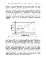
Figure 5.8 Conventional SRAM (a) static-noise margin and (b) bit-line leakage
with respect to supply voltage. (© [2007] IEEE)
Relating these effects to SRAMs, variation in the 6T cell of Figure 5.8a
can skew the relative strength of the pull-down devices, M1/M2, which
104 Yogesh K. Ramadass, Joyce Kwong, Naveen Verma, Anantha Chandrakasan
must be stronger than the access devices, M5/M6, for correct read opera-
tion. The transfer curves from NT–NC and NC–NT are shown for various
V
DD
’s; in all cases, they nominally intersect at two stable points near V
DD
and ground, representing the storable data states, as well as one metastable
point at mid-V
DD
. However, if variation is severe enough to skew both
transfer curves by an amount equal to the edge length of the largest em-
bedded square, called the static-noise margin (SNM), one of the required
storage states is lost [14]. While the read SNM is precariously degraded at
low voltages, Figure 5.8a shows that the hold SNM, which considers the
case where the word-line (WL) is low, can be more easily retained. Simi-
larly, the reduced on-to-off ratio of the device currents at low voltages has
the problematic effect shown in Figure 5.8b, where the leakage currents
from the unaccessed cells sharing the bit-lines can exceed the read-current
from the accessed cell. As a result, the droop on the two bit-lines is indis-
tinguishable. The following sections describe circuit techniques to address
these limitations.
5.2.1 Low-Voltage Bit-Cell Design
As described above, low-voltage operation requires an improvement in
both read SNM, to avoid bit flipping, and read-current, to avoid sensing
failures due to bit-line leakage. Unfortunately, however, the 6T bit-cell,
shown in Figure 5.8a, imposes an inherent trade-off between these two.
This comes about as a result of the access devices, M5/M6, which should
be weak for good read SNM but strong for good read-current. Of course,
the pull-down devices can be strengthened; however, soft gate-oxide
breakdown effects in these devices oppose an improvement in the read
SNM [15, 16], and the area increase required to manage variation is over-
whelming.
Alternatively, the 8T bit-cell shown in Figure 5.9 uses a read-buffer
(M7/M8) to break the trade-off between read SNM and read-current. Of
course, the addition of extra devices can result in reduced density; how-
ever, the resulting structure can be free of the read SNM limitation, and its
minimum operating voltage can be set by the hold SNM, which, as men-
tioned, is preserved to very low voltages.
Chapter 5 Adaptive Supply Voltage Delivery for U-DVS Systems 105
0.2 0.4 0.6 0.8 1
1.4
1.6
1.8
2
2.2
2.4
2.6
2.8
3
4σ Read−Current Gain (A/A)
V
DD
(V)
50% Width
Increase
25% Width
Increase
0.2 0.4 0.6 0.8 1
1
1.5
2
2.5
3
3.5
4
4.5
5
4σ Read−Current Gain (A/A)
V
DD
(V)
80% Length
Increase
40% Length
Increase
Figure 5.9 8T bit-cell with a 2 transistor read-buffer formed by M7/M8.
(© [2007] IEEE)
Lastly, for an ultra-dynamic voltage scaling design, it is important to
note that the trade-off between cell area and read-current/read SNM
changes dramatically with operating voltage. Specifically, Figure 5.10
shows the improvement in 4σ read-current at low voltages as a result of
read-buffer upsizing. Consequently, as the performance of reduced voltage
modes in an application becomes more critical, device upsizing has en-
hanced appeal.
(a) (b)
Figure 5.10 4-σ read-current gain due (a) width upsizing and (b) length upsizing
of read-buffer devices. (© [2007] IEEE)
5.2.2 Periphery Design
Since the trade-off between read-current and read SNM is built into the 6T
cell as a result of the access devices, the bit-cell itself must be modified to
simultaneously address those limitations at low operating voltages. Most
106 Yogesh K. Ramadass, Joyce Kwong, Naveen Verma, Anantha Chandrakasan
0.1 0.2 0.3 0.4
0
0.1
0.2
0.3
0.4
0.5
0.6
Cell Supply (V)
Min. WL Voltage (V)
Mean
3σ
4σ
VV
DD
(float or drive low)
WL
BL/BLB
VV
DD
NT/NC
NTNC
BLB=“0” BL=“1”
WL=“1”
Weaken PMOS loads
other limitations, however, can be addressed using peripheral or architec-
tural assists that impose minimal density penalty.
Figure 5.11 Reducing cell supply eases strength requirement of access devices, as
reflected by reduction in minimum word-line voltage required for successful
write. (© [2007] IEEE)
For instance, enhanced error correction coding (ECC) is required in or-
der to take full advantage of the 8T cell’s wider operating margin (i.e.,
hold SNM instead of read SNM). Soft-errors exhibit spatial locality, so
SRAMs conventionally employ column-interleaved layouts to avoid multi-
bit errors in logical words. During write operations, some cells are row se-
lected but not column selected (commonly called half-accessed cells), and,
consequently, they must be read SNM stable. Alternatively, in non-
interleaved layouts [13], only cells from the addressed word need to be se-
lected, and no read SNM limitation exists. However, since bits from a
logical word are adjacent, additional ECC complexity is required to toler-
ate multi-bit soft-errors [17].
An additional difficulty during write operations arises from device
variation increasing the strength of the pull-up devices, which must be
overcome by the access devices in order to ensure successful write. How-
ever, the required relative strengths can be enforced; for example, the
word-line voltage can be boosted above V
DD
, or the appropriate bit-line
voltage can be pulled below ground to strengthen the access devices. Un-
fortunately, both of these strategies involve the complexity of driving a
large capacitance beyond one of the rail voltages. Instead, the bit-cell sup-
ply voltage can be floated [18] or driven low [13] to weaken the pull-up
PMOS load devices. Figure 5.11 shows that as the cell supply, VV
DD
, is
reduced, the strength requirement of the access device during a write op-
eration is reduced, which is represented by a decrease in the minimum
word-line voltage that still results in a successful write.
Chapter 5 Adaptive Supply Voltage Delivery for U-DVS Systems 107
Figure 5.12 Read-buffer foot-driver limitation can be alleviated in sub-V
t
designs
by driving the peripheral footer with a charge-pump circuit. (© [2007] IEEE)
Finally, the problematic sub-threshold leakage currents from the unac-
cessed cells that result in excessive bit-line leakage can be eliminated by
pulling the foot of the 8T cell read-buffer up to V
DD
. Of course this im-
poses a severe current drive requirement on the peripheral foot driver
shown in Figure 5.12, since, when accessed, it must sink the read-current
from all cells in the row. For sub-threshold supply voltages, the peripheral
footer can be driven with a charge-pump circuit, resulting in an exponen-
tial increase in its drive strength [13]. This technique, however, does not
scale well to higher voltages in a U-DVS system. Nonetheless, despite the
overhead, footer upsizing is a practical solution in this case since the cell
read-current is dominantly limited by the bit-cells themselves which face
up to 5σ degradation. The foot driver can be much larger, thereby suffering
much less degradation from variation, and since it is in the periphery, only
2 or 3σ degradation must be attributed.
5.3 Intelligent Power Delivery
5.3.1 Deriving V
DD
for Given Speed Requirement
To effectively use DVS to reduce power consumption, a system controller
that determines the required operating speed of the processor at run-time is
needed. The system controller makes use of algorithms, termed voltage
schedulers, to determine the operating speed of the processor at run-time.
For general-purpose processors, these algorithms effectively determine the
overall workload of the processor and suggest the required operating speed
108 Yogesh K. Ramadass, Joyce Kwong, Naveen Verma, Anantha Chandrakasan
to handle the user requests. Some of the commonly used algorithms have
been described in [19]. For DSP systems like video processors, the speed
of the system is typically measured by looking at the buffer length occu-
pied. Once this operating speed has been determined, the operating voltage
of the circuit needs to be changed so that it can meet the required speed of
operation.
The simplest way to change the rate of the processor is to let it operate
at full speed for a fraction of the time and to then shut it down completely.
The fixed power supply curve in Figure 5.1a shows the linear energy sav-
ings that can be obtained by this process. A variable supply voltage on the
other hand can provide with super-linear savings in energy consumed. The
curve with infinite allowable levels provides the optimum curve for reduc-
ing energy. The change in supply voltage can be achieved through several
means. Supply voltage dithering, which uses discrete voltage and fre-
quency pairs, was proposed as a solution to achieve DVS [1]. Local volt-
age dithering (LVD) [20] improves on existing voltage dithering systems
by taking advantage of faster changes in workload and by allowing each
block to optimize based on its own workload. While dithering can provide
close to the optimal savings in energy consumed, it requires an efficient
system controller that can time-share between the different voltage levels
adding to the overall complexity of the system. This is of specific concern
in ultra-low-power applications. Also, voltage dithered systems that
achieve U-DVS require at least two voltage levels different from the bat-
tery voltage to achieve the stated power savings. This increases the number
of DC–DC converters to supply these voltage levels.
Having a DC–DC converter that can supply scalable voltages as de-
manded by the system it is catering to can be of great advantage in terms
of both simplicity of the overall solution and cost. This requires a DC–DC
converter that can firstly deliver variable load voltages. A suitable control
strategy is needed to change the load voltage supplied by the DC–DC con-
verter to maintain the operating speed. Reference [21] presents a closed
loop architecture to change the output voltage of a voltage scalable DC–
DC converter to make the load circuit operate at the desired rate. Refer-
ence [1] uses a hybrid approach employing both look-up tables and a
phase-locked loop (PLL) to enable fast transitions in load voltage with
change in the desired rate. While the look-up table aids in the fast transi-
tion, the PLL helps in tracking process variations and operating conditions.
Both these approaches use switching regulators with off-chip inductors.
The next section talks about some of the commonly used topologies for U-
DVS DC–DC converters.
Chapter 5 Adaptive Supply Voltage Delivery for U-DVS Systems 109
5.3.2 DC–DC Converter Topologies for U-DVS
5.3.2.1 Linear Regulators
Low-dropout (LDO) linear regulators [22] are widely used to supply ana-
log and digital circuits and feature in several standalone or embedded
power management ICs. The main advantage of LDO’s is that they can be
completely on-chip, occupy very little area, and offer good transient and
ripple characteristics, together with being a low-cost solution. Using
LDO’s for U-DVS, however, is detrimental because of the linear loss of
efficiency in an LDO. A linear regulator essentially controls the resistance
of a transistor in order to regulate the output voltage. As a result, the cur-
rent delivered to the load flows directly from the battery and hence the
maximum efficiency achievable is limited to the ratio of the output voltage
to the input voltage. Thus, the farther away the load voltage is from the
battery voltage, the lower the efficiency of the LDO. This hampers the po-
tential savings in power consumption that can be achieved by lowering the
voltage through DVS.
5.3.2.2 Inductor-Based DC–DC Converter
The most efficient DC–DC voltage converters are inductor-based switch-
ing regulators, which normally generate a reduced DC voltage level by fil-
tering a pulse-width modulated (PWM) signal through a simple LC filter.
A buck-type regulator can generate different DC voltage levels by varying
the duty-cycle of the PWM signal. Given ideal devices and passives, an
inductor-based DC–DC converter can theoretically achieve 100% effi-
ciency independent of the load voltage being delivered. Moreover, in the
context of DVS systems, scaling the output voltage can be done with com-
pletely digital control circuitry [21] which consumes very little overhead
power. An implementation of an inductor-based switching regulator for
minimum energy operation is described in Section 5.3.3.1C. While buck
converters [23] can operate at very high efficiencies (>90%), they gener-
ally require off-chip filter components. This might limit their usefulness
for integrated power converter applications. Integrating the filter inductor
on-chip requires very high switching frequencies (>100MHz) in order to
minimize area consumed. This increases the switching losses in the con-
verter and together with the increase in conduction losses due to the low
inductor Q-factors achievable on-chip severely affects the efficiency that
can be obtained out of the converter.
110 Yogesh K. Ramadass, Joyce Kwong, Naveen Verma, Anantha Chandrakasan
5.3.2.3 Switched Capacitor-Based DC–DC Converter
U-DVS systems often require multiple on-chip voltage domains with each
domain having specific power requirements. A switched capacitor (SC)
DC–DC converter is a good choice for such battery-operated systems be-
cause it can minimize the number of off-chip components and does not re-
quire any inductors. Previous implementations of SC converters (charge
pumps) have commonly used off-chip charge-transfer capacitors [24] to
output high load power levels. A SC DC–DC converter which integrates
the charge-transfer capacitors was described in [25].
C
load
I
O
V
O
= V
NL
−ΔV
C
C
V
BAT
Φ
1
Φ
2
Φ
2
Φ
1
Φ
2
C
load
I
O
V
O
= V
NL
−ΔV
C
C
V
BAT
Φ
1
Φ
2
Φ
2
Φ
1
Φ
2
Figure 5.13 A switched capacitor voltage divide-by-2 circuit.
Consider the divide-by-2 circuit shown in Figure 5.13. The charge-
transfer (flying) capacitors are equal in value and help in transferring
charge from the battery to the load. During phase Φ
1
of the system clock,
the charge-transfer capacitors get charged from the battery (V
BAT
). In the
Φ
2
phase of the clock, they dump the charge gained onto the load. At no
load, this circuit tries to maintain the output voltage V
O
at V
BAT
/2, where
V
BAT
is the battery voltage. The actual value of V
O
that the circuit settles
down to is dependent on the load current I
O
, the switching frequency, and
C. Let the circuit deliver a load voltage V
O
= V
NL
– ΔV, where V
NL
is the
no-load voltage for this topology. The SC converter limits the maximum
efficiency that can be achieved in this case to
η
lin
= (1 – ΔV/V
NL
). Thus,
the farther away V
O
is from V
NL
(i.e., higher ΔV), the smaller the maxi-
mum efficiency that can be achieved by this topology. This is a fundamen-
tal problem with charge transfer using only capacitors and switches. The
linear efficiency loss is similar to linear regulators. However, with SC
converters, it is possible to switch in different gain-settings whose no-load
Chapter 5 Adaptive Supply Voltage Delivery for U-DVS Systems 111
output voltage is closer to the load voltage desired. Apart from the linear
conduction loss, losses due to bottom-plate parasitics of on-chip capacitors
and switching losses limit the efficiency of the SC DC–DC converter [26].
The efficiency achievable in a switched capacitor system is in general
smaller than that can be achieved in an inductor-based switching regulator
with off-chip passives. Furthermore, multiple gain-settings and associated
control circuitry are required in a SC DC–DC converter to maintain effi-
ciency over a wide voltage range. However, for on-chip DC–DC convert-
ers, a SC solution might be a better choice, when the trade-offs relating to
area and efficiency are considered. Furthermore, the area occupied by the
switched capacitor DC–DC converter is scalable with the load power de-
mand, and hence the switched capacitor DC–DC converter is a good solu-
tion for low-power on-chip applications.
SWITCH
MATRIX
I
O
V
O
V1p8
V
BAT
(1.2V)
Φ
1
Φ
2
Φ
1by3
Φ
2by3
enW2
enW4
Non-Overlapping
Clock Generator
V
ref
clk
COMP
C
load
AUTOMATIC
FREQUENCY
SCALER
V
O
Φ
2
clk4X
DAC
clk
÷
V
ref
Φ
1
Φ
2
Φ
1by3
Φ
2by3
7
SWITCH
MATRIX
I
O
V
O
V1p8
V
BAT
(1.2V)
Φ
1
Φ
2
Φ
1by3
Φ
2by3
enW2
enW4
Non-Overlapping
Clock Generator
V
ref
clk
COMP
C
load
AUTOMATIC
FREQUENCY
SCALER
V
O
Φ
2
clk4X
DAC
clk
÷
V
ref
Φ
1
Φ
2
Φ
1by3
Φ
2by3
7
Figure 5.14 Architecture of a switched capacitor DC–DC converter with on-chip
charge-transfer capacitors. (© [2007] IEEE)
A SC DC–DC converter that employs five different gain-settings with
ratios 1:1, 3:4, 2:3, 1:2, and 1:3, is described in [26]. The switchable gain-
settings help the converter to maintain a good efficiency as the load volt-
age delivered varies from 300mV to 1.1V. Figure 5.14 shows the architec-
ture of the SC DC–DC converter. At the core of the system is the switch
matrix which contains the charge-transfer capacitors and the charge-
transfer switches. A suitable gain-setting is chosen depending on the refer-
ence voltage V
ref
, which is set digitally. A pulse frequency modulation
(PFM) mode control is used to regulate the output voltage to the desired
value. Bottom-plate parasitics of the on-chip capacitors significantly affect
the efficiency of the converter. A divide-by-3 switching scheme [26] was
employed to mitigate the effect due to bottom-plate parasitics and improve
efficiency. The switching losses are scaled with change in load power by
112 Yogesh K. Ramadass, Joyce Kwong, Naveen Verma, Anantha Chandrakasan
the help of the automatic frequency scaler block. This block changes the
switching frequency as the load power delivered changes, thereby reducing
the switching losses at low load.
The efficiency of the SC converter with change in load voltage while
delivering 100μW to the load from a 1.2V supply is shown in Figure 5.15.
The converter was able to achieve >70% efficiency over a wide range of
load voltages. An increase in efficiency of close to 5% can be achieved by
using divide-by-3 switching.
0.3 0.4 0.5 0.6 0.7 0.8 0.9 1 1.1
50
55
60
65
70
75
80
85
90
95
Load Voltage (V)
Efficiency (%)
Measured - divby3 switching
Measured - normal switching
Theoretical
0.3 0.4 0.5 0.6 0.7 0.8 0.9 1 1.1
50
55
60
65
70
75
80
85
90
95
Load Voltage (V)
Efficiency (%)
Measured - divby3 switching
Measured - normal switching
Theoretical
Figure 5.15 Efficiency of the switched capacitor DC–DC converter with change
in load voltage. (© [2007] IEEE)
5.3.3 DC–DC Converter Design and Reference Voltage
Selection for Highly Energy-Constrained Applications
While dynamic voltage scaling is a popular method to minimize power
consumption in digital circuits given a performance constraint, the same
circuits are not always constrained to their performance-intensive mode
during regular operation. There are long spans of time when the perform-
ance requirement is highly relaxed. There are also certain emerging en-
ergy-constrained applications where minimizing the energy required to
complete operations is the main concern. For both these scenarios, operat-
ing at the minimum energy operating voltage of digital circuits has been
proposed as a solution to minimize energy. The minimum energy point
Chapter 5 Adaptive Supply Voltage Delivery for U-DVS Systems 113
(MEP) is defined as the operating voltage at which the total energy con-
sumed per desired operation of a digital circuit is minimized. Switching
energy of digital circuits reduces quadratically as V
DD
is decreased below
V
T
(i.e., sub-threshold operation), while the leakage energy increases ex-
ponentially. These opposing trends result in the minimum energy point.
The MEP is not a fixed voltage for a given circuit and can vary widely de-
pending on its workload and environmental conditions (e.g., temperature).
Any relative increase in the active energy component of the circuit due to
an increase in the workload or activity of the circuit decreases the mini-
mum energy operating voltage. On the other hand, a relative increase of
the leakage energy component due to an increase in temperature or the du-
ration of leakage over an operation pushes the minimum energy operating
voltage to go up. This makes the circuit go faster, thereby not allowing the
circuit to leak for a longer time. By tracking the MEP as it varies, energy
savings of 50–100% has been demonstrated [27] and even greater savings
can be achieved in circuits dominated by leakage. This motivates the de-
sign of a minimum energy tracking loop that can dynamically adjust the
operating voltage of arbitrary digital circuits to their MEP.
5.3.3.1 Minimum Energy Tracking Loop
Figure 5.16 shows the architecture of the minimum energy tracking loop.
The objective of this loop is to track the minimum energy operating
voltage of the load circuit. The load circuit (FIR filter) is powered from an
off-chip voltage source through a DC–DC converter and is clocked by a
CLK
var
V
DD
V
ref
Energy
Sensor
Circuitry
Load
(FIR Filter)
DC-DC
Converter
and Control
Energy
Minimization
Algorithm
Critical Path
Replica Ring
Oscillator
COMP
Energy /
operation
DAC
C
load
AV
ref
V
DD
V
BAT
7
13
CLK
var
V
DD
V
ref
Energy
Sensor
Circuitry
Load
(FIR Filter)
DC-DC
Converter
and Control
Energy
Minimization
Algorithm
Critical Path
Replica Ring
Oscillator
COMP
Energy /
operation
DAC
C
load
AV
ref
V
DD
V
BAT
7
13
Figure 5.16 Architecture of the minimum energy tracking loop. (© [2007] IEEE)
114 Yogesh K. Ramadass, Joyce Kwong, Naveen Verma, Anantha Chandrakasan
critical path replica ring oscillator which automatically scales the clock
frequency of the FIR filter with change in load voltage. The energy sensor
circuitry calculates on-chip, the energy consumed per operation of the load
circuit at a particular operating voltage. It then passes the estimate of the
energy/operation (E
op
) to the energy minimizing algorithm, which uses the
E
op
to suitably adjust the reference voltage to the DC–DC converter. The
DC–DC converter then tries to get V
DD
close to the new reference voltage,
and the cycle repeats till the minimum energy point is achieved. The only
off-chip components of this entire loop are the filter passives of the induc-
tor-based switching DC–DC converter.
A. Energy Sensing Technique
The key element in the minimum energy tracking loop is the energy sensor
circuit which computes the E
op
of the load circuit at a given reference volt-
age. Methods to measure E
op
, by sensing the current flow through the DC–
DC converter’s inductor [28], dissipate a significant amount of overhead
power. The approach is more complicated at sub-threshold voltages be-
cause the current levels are very low. Furthermore, an estimate of the en-
ergy consumed per operation is what is required and not just the current
which only gives an idea of the load power. The methodology used here, to
estimate E
op
, does not require any high-gain amplifiers or analog circuit
blocks.
The DC–DC converter while operating in steady state keeps the output
voltage close to the reference voltage. Just before the energy sense cycle
begins, the DC–DC converter is disabled. The energy sense cycle consists
of N operations of the digital circuit where the value N can be 32 or 64.
Assuming that the voltage across the storage capacitor of the DC–DC con-
verter, C
load
, falls from the reference voltage V
1
to V
2
in the course of N op-
erations of the digital circuit, E
op
at the voltage V
1
is equal to
( )
N2
V
2
2
2
−
=
1load
op
V C
E
(5.1)
To measure E
op
accurately, V
2
should be close in value (within 20mV) to
V
1
. Measuring E
op
by digitizing V
1
and V
2
using conventional ADCs would
require at least 11 bits of precision in the ADC. This could prove costly in
terms of power consumed. An energy-efficient approach to obtain E
op
is to
observe that, by design, V
1
is very close to V
2
. Thus, the following simpli-
fication can be applied within an acceptable error:
Chapter 5 Adaptive Supply Voltage Delivery for U-DVS Systems 115
()() ()
NN2
211load2121load
op
VVVC VV VV C
E
−
≈
−+
=
(5.2)
()
211op
VVVE −∝
(5.3)
From Equation (5.3), it can be seen that the energy consumed per opera-
tion is directly proportional to the product of V
1
and V
1
– V
2
. Since, the
digital representation of V
1
, which is the reference voltage to the DC–DC
converter, is already known, only the digital value for the voltage differ-
ence (V
1
– V
2
)
is required to estimate E
op
. This voltage difference is ob-
tained digitally using a fixed frequency clock, a constant current sink, a
comparator, and a counter [27]. These blocks help in quantizing voltage
into time steps, as in an integrating ADC [29]. The number of fixed fre-
quency clock cycles obtained from the counter is directly proportional to
V
1
– V
2
. This quantity is then digitally multiplied with V
1
which is the ref-
erence voltage V
ref
to the DC–DC converter. The product of these two
quantities gives an estimate of the energy consumed per operation by the
digital circuit at voltage V
1
. The estimate obtained is a normalized repre-
sentation of the absolute value of the energy consumed per operation. This
estimate is passed on to the energy minimization algorithm block.
B. Energy Minimization Algorithm
Once the estimate of the energy per operation is obtained, the minimum
energy tracking algorithm uses this to suitably adjust the reference voltage
to the DC–DC converter. The minimum energy tracking algorithm is a
slope-tracking algorithm which makes use of the single minimum, concave
nature of the E
op
versus V
DD
curve (see Figure 5.1b). The algorithm starts
by setting the reference voltage V
ref
to some initial value. The energy per
operation at this voltage is computed and stored in a minimum energy reg-
ister (E
op,min
). The tracking loop then automatically increments V
ref
by one
voltage step. Once V
DD
settles at this newly incremented voltage, E
op
is
computed again and is compared with the value stored in the minimum en-
ergy register. At this point, if the newly computed E
op
is found to be
smaller, the loop then just keeps incrementing V
ref
at fixed voltage steps,
while at the same time updating E
op,min
till the minimum is achieved. The
other possibility is that the newly computed energy per operation is higher
than that stored in the minimum energy register. In this case, the loop
changes direction and begins to decrement V
ref
. The loop keeps decrement-
ing V
ref
till the E
op
calculated is higher than E
op, min
at which time the loop
116 Yogesh K. Ramadass, Joyce Kwong, Naveen Verma, Anantha Chandrakasan
increments V
ref
by one voltage step to get to the MEP and shuts down.
Figure 5.17 shows the minimum energy tracking loop in operation for a
7-tap FIR filter load circuit.
The voltage step used by the tracking algorithm is usually set to 50mV.
A large voltage step leads to coarse tracking of the MEP, with the possibil-
ity of missing the MEP. On the other hand, keeping the voltage step too
small might lead to the loop settling at the non-minimum voltage due to er-
rors involved in computing E
op
[30]. The E
op
versus V
DD
curve is shallow
near the MEP, and hence a 50mV step leads to a very close approximation
of the actual minimum energy consumed per operation. The MEP tracking
loop can be enabled by a system controller as needed depending on the ap-
plication, or periodically by a timer to track temperature variations.
V
DD
Loop Start
Loop Stop
V
DD
starts at 420mV V
DD
settles at 370mV
370mV
320mV
V
DD
Loop Start
Loop Stop
V
DD
starts at 420mV V
DD
settles at 370mV
370mV
320mV
Figure 5.17 Measured waveform showing the minimum energy tracking loop in
operation. (© [2007] IEEE)
Chapter 5 Adaptive Supply Voltage Delivery for U-DVS Systems 117
C. Embedded DC–DC Converter for Minimum Energy Operation
This section talks about the design of the DC–DC converter that enables
minimum energy operation. Since the minimum energy operating voltage
usually falls in the sub-threshold regime of operation, the DC–DC con-
verter is designed to deliver load voltages from 250mV to around 700mV.
The power consumed by digital circuits at these sub-threshold voltages is
exponentially smaller and hence the DC–DC converter needs to deliver ef-
ficiently load power levels of the order of micro-watts. This demands ex-
tremely simple control circuitry design with minimal overhead power to
get good efficiency. The DC–DC converter shown in Figure 5.18 is a syn-
chronous rectifier buck converter with off-chip filter components and op-
erates in the discontinuous conduction mode (DCM). It employs a pulse
frequency modulation (PFM) [31] mode of control in order to get good ef-
ficiency at the ultra-low load power levels that the converter needs to de-
liver. The PFM mode control also helps in seamlessly disabling the con-
verter when energy sensing takes place, thereby making it feasible to use
the energy-sensing technique described in Section 5.3.3.1A.
The reference voltage to the converter is set digitally by the minimum
energy tracking loop and is converted to an analog value by an on-chip
DAC before it is fed to the comparator. The comparator compares V
DD
with this reference voltage and when V
DD
is found to be smaller generates
a pulse of fixed width to turn the PMOS power transistor ON and ramp up
the inductor current. A variable pulse-width generator to achieve zero-
current switching is used for the NMOS power transistor. The comparator
is clocked by a divided and level-converted version of the system clock
which feeds the load FIR filter.
CLK
var
V
BAT
(1.2V)
AV
ref
COMP
Off-chip
L
C
load
כ
כ
כ
כ
EN
Fixed
Pulse Width
Generator
Variable
Pulse Width
Generator
V
ref
V
DD
Divider and Level
Converter
(from DAC)
CLK
var
V
BAT
(1.2V)
AV
ref
COMP
Off-chip
L
C
load
כ
כ
כ
כ
EN
Fixed
Pulse Width
Generator
Variable
Pulse Width
Generator
V
ref
V
DD
Divider and Level
Converter
(from DAC)
Figure 5.18 DC–DC Converter architecture. (© [2007] IEEE)
118 Yogesh K. Ramadass, Joyce Kwong, Naveen Verma, Anantha Chandrakasan
V
ref
0
1
2
3
Decoder
τ
1
τ
2
τ
3
τ
4
τ
P
V
BAT
NMOS
PULSE
PMOS
PULSE
i
L
(t)
τ
1
τ
2
τ
4
τ
3
Variable Pulse-Width Generator
V
ref
0
1
2
3
Decoder
τ
1
τ
2
τ
3
τ
4
τ
P
V
BAT
NMOS
PULSE
PMOS
PULSE
i
L
(t)
τ
1
τ
2
τ
4
τ
3
τ
P
V
BAT
NMOS
PULSE
PMOS
PULSE
i
L
(t)
τ
1
τ
2
τ
4
τ
3
Variable Pulse-Width Generator
Figure 5.19 Approximate zero-current switching block. (© [2007] IEEE)
The ultra-low load power levels demand extremely simple control cir-
cuitry to achieve good efficiency. This precludes the usage of high-gain
amplifiers to detect zero-crossing and thereby do zero-current switching
[31]. In order to keep the control circuitry simple and consume little over-
head power, an all-digital open-loop control as shown in Figure 5.19 is
used to achieve zero-current switching. The variable pulse-width generator
block which accomplishes this functions as follows: When the comparator
senses that V
DD
has fallen below the reference voltage, a PMOS ON pulse
of fixed pulse width τ
P
is generated. This ramps up the inductor current
from zero. Once the PMOS is turned OFF, the NMOS power transistor is
turned ON after a fixed delay. This ramps down the inductor current. Ide-
ally, in the discontinuous conduction mode (DCM) used in this implemen-
tation, the NMOS has to be turned OFF just when the inductor current
reaches zero. The amount of time it takes for the inductor current to reach
zero is dependent on the reference voltage set, and in steady state, the ratio
of the NMOS to PMOS ON-times is given by the following equation:
DD
DDBAT
P
N
V
VV −
=
τ
τ
(5.4)
where τ
N
and τ
P
are the NMOS and PMOS ON-times and V
BAT
is the bat-
tery voltage. Thus, by fixing τ
P
, the values of τ
N
for specific load voltages
can be predetermined. The variable pulse-width generator block then
suitably multiplexes these predetermined delays depending on the refer-
ence voltage set to achieve approximate zero-current switching. Increasing
the number of these delay elements and the complexity of the multiplexer
block gives a better approximation to zero-current switching. Since only
the ratios of the NMOS and PMOS ON-time pulse widths need to match,
this scheme is independent of absolute delay values and any tolerance in
the inductor value. Furthermore, it consumes very little overhead power.
Chapter 5 Adaptive Supply Voltage Delivery for U-DVS Systems 119
1 10 100
60
65
70
75
80
85
90
Load Power (
μ
W)
Efficiency (%)
Figure 5.20 Efficiency of the inductor-based switching regulator embedded within
the minimum energy tracking loop. (© [2007] IEEE)
With the help of the above-mentioned efficiency improvement tech-
niques, the DC–DC converter was able to achieve an efficiency >80% at
an extremely low load power level of 1μW as shown in Figure 5.20. While
the switching and conduction losses bring down efficiency at load power
levels of 100μW and above, the leakage losses kick in at lower load levels
bringing the efficiency further down. The simplicity of the control blocks
helps to maintain good efficiency at these ultra-low load power levels.
The proposed minimum energy tracking loop is non-intrusive, thereby
allowing the load circuit to operate without being shut down. At the same
time, it computes the energy per operation of the actual circuit and not of
any replica. This eliminates the problems of designing a replica circuit that
can track the energy behavior of a load circuit over varying operating con-
ditions. The tracking methodology is independent of the size and type of
digital circuit being driven and the topology of the DC–DC converter.
5.4 Conclusion
Dynamic voltage scaling is a popular method to minimize power consump-
tion in digital circuits given a performance constraint. By introducing the
capability of sub-threshold operation, DVS systems can be made to operate
120 Yogesh K. Ramadass, Joyce Kwong, Naveen Verma, Anantha Chandrakasan
at their minimum energy operating voltage in periods of very little activity,
leading to further savings in total energy consumed. These U-DVS systems
provide energy savings by either reducing the supply voltage to just meet
performance or operating at the minimum energy operating voltage in pe-
riods of very little activity.
The challenges involved in designing logic and memory circuits suitable
for sub-threshold operation and the methodology to overcome these chal-
lenges have been described in this chapter. Furthermore, a control circuit
to track the optimum energy point of digital circuits was presented. The
DC–DC converter used within the control loop was designed to provide
sub-threshold output voltages at very high efficiencies. The overall design
methodology and the control circuit help in saving energy consumed in
highly energy-critical applications leading to enhanced battery lifetimes
and the ability to operate out of scavenged energy.
References
[1] V. Gutnik and A. Chandrakasan, “Embedded power supply for low-power
DSP,” IEEE Trans. VLSI Syst., vol. 5, no. 4, pp. 425–435, Dec. 1997.
[2] A. Sinha and A. Chandrakasan, “Dynamic power management in wireless
sensor networks,” IEEE Design and Test of Computers, vol. 18, no. 2, pp.
62–74, March 2001.
[3] B. Zhai et al., “A 2.6pJ/Inst subthreshold sensor processor for optimal en-
ergy efficiency,” in Symp. VLSI Circuits Tech. Dig., pp. 192–193, June 2006.
[4] O. Soykan, “Power sources for implantable medical devices,” Medical
Device Manufacturing and Technology, 2002.
[5] S. Roundy, P. K. Wright, and J. Rabaey, “A study of low level vibrations as
a power source for wireless sensor nodes,” Computer Communications, vol.
26, no. 11, pp. 1131–1144, July 2003.
[6] A. Wang and A. Chandrakasan, “A 180-mV Sub-threshold FFT processor
using a minimum energy design methodology,” IEEE J. Solid-State Circuits,
vol. 40, no. 1, pp. 310–319, Jan. 2005.
[7] A. Wang, B. H. Calhoun, and A. P. Chandrakasan, “Sub-Threshold Design
for Ultra Low-Power Systems,” New York, Springer, pp. 75-–102, 2006.
[8] M. J. M. Pelgrom, A. C. J. Duinmaijer, and A. P. G. Welbers, “Matching
properties of MOS transistors,” IEEE J. Solid-State Circuits, vol. 24, no. 5,
pp. 1433–1439, Oct. 1989.
[9] J. Kwong, A. P. Chandrakasan, “Variation-driven device sizing for minimum
energy sub-threshold circuits,” IEEE Intl. Symp. on Low Power Electronics
and Design, 2006. pp. 8–13.
[10] A. Srivastava, D. Sylvester, D. Blaauw, “Statistical analysis and optimization
for VLSI: timing and power,” New York, Springer, pp. 79–132, 2005.
Chapter 5 Adaptive Supply Voltage Delivery for U-DVS Systems 121
[11] B. Zhai, S. Hanson, D. Blaauw, and D. Sylvester, “Analysis and mitigation
of variability in subthreshold design,” IEEE Intl. Symp. on Low Power Elec-
tronics and Design, pp. 20–25, 2005.
[12] J. Pille et al., “Implementation of the CELL broadband engine in a 65nm SOI
technology featuring dual-supply SRAM arrays supporting 6GHz at 1.3V,”
IEEE ISSCC Dig. Tech. Papers, pp. 322–323, Feb. 2007.
[13] N. Verma and A. Chandrakasan, “A 65nm 8T sub-V
t
SRAM employing
sense-amplifier redundancy,” IEEE ISSCC Dig. Tech. Papers, pp. 328–329,
Feb. 2007.
[14] E. Seevinck, F. List and J. Lohstroh, “Static noise margin analysis of MOS
SRAM cells,” IEEE J. Solid-State Circuits, vol. SC-22, no. 5, pp. 748–754,
Oct. 1987.
[15] M. Agostinelli, et al., “Erratic fluctuations of SRAM cache Vmin at the
90nm process technology node,” IEDM Dig. Tech. Papers, pp. 671–674,
Dec. 2005.
[16] R. Rodriguez, et al. “The impact of gate-oxide breakdown on SRAM stabil-
ity,” IEEE Electron Device Letters, vol. 23, no. 9, pp. 559–561, Sept. 2002.
[17] L. Chang, et al., “A 5.3GHz 8T-SRAM with operation down to 0.41V in
65nm CMOS,” Symp. VLSI Circuits, pp. 252–253, June 2007.
[18] B. Calhoun and A. Chandrakasan, “A 256kb sub-threshold SRAM in 65nm
CMOS,” IEEE ISSCC Dig. Tech. Papers, pp. 628–629, Feb. 2006.
[19] T. Pering, T. Burd and R. Brodersen, “The simulation and evaluation of dy-
namic voltage scaling algorithms,” IEEE Intl. Symp. Low Power Electronics
and Design, pp. 76–81, 1998.
[20] B. H. Calhoun and A. P. Chandrakasan, “Ultra-dynamic voltage scaling us-
ing sub-threshold operation and local voltage dithering in 90nm CMOS,”
IEEE ISSCC Dig. Tech. Papers, pp. 300–301, Feb. 2005.
[21] G-Y.Wei and M. Horowitz, “A fully digital, energy-efficient, adaptive
power-supply regulator,” IEEE J. Solid-State Circuits, vol. 34, no. 4,
pp. 520–528, Apr. 1999.
[22] P. Hazucha et al., “Area efficient linear regulator with ultra-fast load regula-
tion,” IEEE J. Solid-State Circuits, vol. 40, no. 4, pp. 933–940, Apr. 2005.
[23] J. Xiao, A. Peterchev, J. Zhang and S. Sanders, “A 4μA-quiescent-current
dual-mode buck converter IC for cellular phone applications,” IEEE ISSCC
Dig. Tech. Papers, pp. 280–281, Feb. 2004.
[24] A. Rao, W. McIntyre, U. Moon and G. C. Temes, “Noise-shaping techniques
applied to switched capacitor voltage regulators,” IEEE J. Solid-State Cir-
cuits, vol. 40, no. 2, pp. 422–429, Feb. 2005.
[25] G. Patounakis, Y. Li and K. L. Shepard, “A fully integrated on-chip DC–DC
conversion and power management system,” IEEE J. Solid-State Circuits,
vol. 39, no. 3, pp. 443–451, Mar. 2004.
[26] Y. K. Ramadass and A. Chandrakasan, “Voltage scalable switched capacitor
DC–DC converter for ultra-low-power on-chip applications,” IEEE Power
Electronics Specialists Conference,
pp. 2353–2359, June 2007.