Báo cáo hóa học: " Analog-Digital Partitioning for Low-Power UWB Impulse Radios under CMOS Scaling" potx
Bạn đang xem bản rút gọn của tài liệu. Xem và tải ngay bản đầy đủ của tài liệu tại đây (1.53 MB, 8 trang )
Hindawi Publishing Corporation
EURASIP Journal on Wireless Communications and Networking
Volume 2006, Article ID 72430, Pages 1–8
DOI 10.1155/WCN/2006/72430
Analog-Digital Partitioning for Low-Power UWB Impulse
Radios under CMOS Scaling
Mustafa Badaroglu,
1
Claude Desset,
2
Julien Ryckaert,
2, 3
Vincent De Heyn,
2
Geert Van der Plas,
2
Piet Wambacq,
2, 3
and Bart Van Poucke
2
1
AMI Semiconductor, 1804 Vilvoorde, Belgium
2
IMEC, 3001 Leuven, Belgium
3
Department of Electronics and Informatics, Vrije Universiteit Brussel, 1050 Brussels, Belgium
Received 2 September 2005; Revised 11 November 2006; Accepted 11 December 2006
Ultra-wideband (UWB) impulse radios show strong advantages for the implementation of low-power transceivers. In this paper,
we analyze the impact of CMOS technology scaling on power consumption of UWB impulse radios. It is shown that the power
consumption of the synchronization constitutes a large portion of the total power in the receiver. A traditional technique to reduce
the power consumption at the receiver is to operate the UWB radios with a very low duty cycle on an architecture with extreme
parallelism. On the other hand, this requires more silicon area and this is limited by the leakage p ower consumption, which
becomes more and more a problem in future CMOS technologies. The proposed quantitative framework allows systematic use of
digital low-power design techniques in future UWB transceivers.
Copyright © 2006 Mustafa Badaroglu et al. This is an open access article distributed under the Creative Commons Attribution
License, which permits unrestricted use, distribution, and reproduction in any medium, provided the orig inal work is properly
cited.
1. INTRODUCTION
UWB impulse radios are good candidates for low-power ra-
dios in sensor networks [1]. They offer lower power commu-
nication due to higher levels of integration and duty cycling,
and the ability to do ranging [2]. In this paper, we focus on
power consumption aspects of integrated UWB impulse ra-
dios.
One possible solution to reduce the power consumption
for the generation of the UWB signals is to gate an oscillator
in the transceiver [3]. Hardware parallelism is employed in
order to process ultra-short pulses in the baseband and to re-
duce the A/D converter (ADC) sampling frequency. In [4]a
low-power reception is achieved using baseband gain blocks
feeding a time-interleaved bank of low-resolution ADCs. Im-
portant drawbacks of employing this parallelism in these ar-
chitectures are the high cost and more power consumption
as a result of increasing number of transistors to realize the
system. Increasing number of transistors also makes the ar-
chitecture more vulnerable to technology scaling. Therefore,
it is important to analyze such tradeoffsinareaandpower
at the system level and to evaluate the benefits of technology
scaling for having a low-power architecture with a well par-
tition between the analog and the digital part.
First attempts to partition the analog and digital part to
reduce the power consumption are described in [5, 6]. In
these architectures, the correlation takes place in the ana-
log part of the receiver. In these architectures, the carrier-
based pulser serves as the transmitter RF front-end and as the
template generator for the analog correlation in the receiver.
However, these architectures rely on extreme parallelism to
perform the acquisition. Therefore, for the acquisition algo-
rithm, a more serial approach is necessary to reduce the hard-
ware complexity. In this case, the architecture should rely on
efficient pipelining schemes in order to keep the preamble
size short enough in order to assure that the clock drift spec-
ifications are met.
The paper compares the power consumption of two ex-
treme impulse UWB radio architectures: (1) an architecture
that fully utilizes a high sampling rate to fully process UWB
pulses in a more parallel baseband; and (2) an architecture
that utilizes analog preprocessing while the symbol corre-
lation is done at the baseband. For this purpose, the pa-
per has chosen two silicon implementations where each well
represents each of these extremes. The experimental results
demonstrate that the latter architecture is more power effi-
cient than full-digital architectures especially at lower data
rates.
2 EURASIP Journal on Wireless Communications and Networking
Direct-downconversion
in quadrature
LNA
I
LO
Q
Baseband pulse
analog correlation
Integrator
ADC
Delay-line and
duty-cycle generator
Digital
baseband
Integrator
ADC
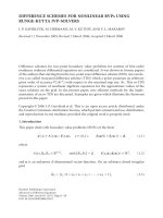
Figure 1: Quadrature correlation receiver architecture.
The paper is organized as follows. In Section 2 ,wede-
scribe the architecture of the UWB transceiver. In Section 3 ,
we present the hardware complexity breakdown of the UWB
digital baseband. In Section 4, we present our numerical re-
sults in order to demonstrate the impact of CMOS tech-
nology scaling on the UWB digital baseband. Finally, in
Section 5, we draw conclusions.
2. UWB TRANSCEIVER ARCHITECTURE
2.1. Transmitter
In the transmitter, the incoming data bits are spread with a
length-N
s
code for code division multiple access and/or for
smoothing the spectrum of the t ransmitted signal. This code
is typically a pseudorandom cyclic code (PN code). Then
the coded sequence enters the pulser, which consists of three
modules: PPM/BPSK modulator, pulse generator, and pulse
shaper, which is responsible for making the pulse compliant
to the FCC spectrum requirements.
As part of the UWB transmitter, in [ 6], we have demon-
strated an integrated 0.18 μm CMOS UWB pulser employing
a triangular pulse shaping. The measurements indicate that
the pulser consumes only 2 mW burst power for a pulse rep-
etition frequency (PRF) of 40 MHz.
2.2. Receiver
The architecture of the receiver is given in Figure 1.Thisar-
chitecture has been introduced in [6, 7]. After giving a short
introduction about the architecture, we will further elaborate
the power consumption of individual modules of the archi-
tecture in addition to the information given in [6]. Theo-
retical details about bit-error-rate (BER) of this architecture
under different channels are described in [8].
The quadrature receiver can be used for both coher-
ent and noncoherent modulation schemes. For BPSK, the
quadrature cross-correlation is required to coherently com-
bine both branches. For PPM, both branches are employed to
extract all energy from the signal. However, for PPM, a cor-
relation must be done at each possible position of the pulse
(2 positions for binary PPM).
The receiver allows the digital baseband to operate at PRF
as suggested in [5, 6]. Therefore, the power consumption of
the digital baseband is significantly reduced. Also further
power reduction is achieved by the fact that all analog blocks
as well as the ADCs operate in a duty-cycle fashion within
a single pulse frame. These dut y-cycle windows should be
properly set by means of the synchronization modules in the
baseband through the duty-cycling and clock generation cir-
cuitry (see Figure 1).
Although the digital signal processing rates have been
significantly reduced and duty-cycling operation reduces the
operation time of analog blocks, the synchronization still re-
mains as a big challenge for a low-power receiver, which will
be described in the next sections.
2.3. Duty-cycling and clock generation
The duty-cycling circuitry is responsible from the generation
of multiphased signals that enable/disable the operation of
the analog blocks in a certain time window. The duty-cycling
circuitry can be realized by cascading two delay lines (DLs)
serially, the first for the PPM delay and the second for setting
the required time window(s) for the analog block(s) under
consideration. The input to the timing circuitry is the system
clock, which has the same frequency as that of the pulses. The
system-clock generation circuitry is composed of a fractional
phase-locked-loop (PLL) and two DLs, one for the coarse ac-
quisition and the other for the tracking.
Coarse acquisition deals with the recovery of the ini-
tial phase of the clock. The coarse acquisition should allow
enough accuracy and cover full frame duration. A bias volt-
agecontrolseachunitdelay.Thebypassswitchesbetween
each delay element allow a digital control on the overall delay
value of DL.
Tracking deals with the compensation of small fre-
quency/phase drifts of the clock in order to maximize the en-
ergy of the received data. In this mode, through a closed-loop
control system, the frequency and phase drifts are handled by
the PLL and the fine DL, respectively.
2.4. Digital baseband for the receiver
The architecture of the digital baseband is given in Figure 2.
It is responsible from the following operations:
(i) bit-level synchronization,
(ii) coarse acquisition for timing offset compensation,
(iii) code-level synchronization,
(iv) phase offset compensation for the I and the Q branch-
es in the constellation (only for BPSK),
(v) tracking to compensate phase/frequency drifts.
During acquisition the correlator is utilized in a cyclic fash-
ion to compute the correlations for every possible alignment
of the PN code. Each correlation result from this computa-
tion is compared to the estimated noise level through a two-
step comparison. For every delay offset the correlation com-
putations and the comparison are iterated. From correlations
computed for every code sequence, the global maximum is
selected in order to estimate the required delay offset to syn-
chronize the phase of the receiver clock to that of the incom-
ing pulse.
Mustafa Badaroglu et al. 3
I1
I2
Q1
Q2
I1
Q1
Cos(ϕ)
Sin(ϕ)
BPSK-noise
PPM-noise/ACQ
MUX
PPM-EOP/data
BPSK-EOP/data
BPSK-ACQ
Operation
mode
Modulation
type
Noise
accum.
I/E-path
sliding
correlator
Q-path
sliding
correlator
Coarse
delay
ThreNO
Sync.
Fine
delay
PC interface
Control
Code
accum.
EOP
detect
Symbol
accum.
RxMem
RxD
ThreEP
Carrier
Offset comp.
Cordic
[atan(Q/I)]
Cordic
Sin, Cos
Cos(ϕ)
Sin(ϕ)
I/C
I
Q
ϕ
+
+
+
+
+
+
+
Figure 2: The architecture of the digital baseband.
For PPM, since the correlation is performed on the dif-
ference of the energies of two different PPM locations, we
only need one correlator. On the other hand, for BPSK, we
need two correlators (for both I and Q branches) since the
carrier phase φ of the received BPSK pulse with respect to
the I branch is unknown. In this case, we recombine the two
correlation outputs afterwards.
The acquisition is costly in terms of hardware and com-
putation time where we have to compute all possible code
rotations. Therefore, the acquisition is more power consum-
ing than the data reception. For a code length of N
s
, the ac-
quisition mode requires 2
·N
s
· T
p
/Δt
c
steps, where T
p
is the
inverse of PRF, and Δt
c
is the unit delay used for setting the
delay offset. For a typical UWB system, we have N
s
= 32,
T
p
= 30 nanoseconds, and Δt
c
= T
m
/2
∼
=
1 nanoseconds,
where T
m
is the pulse duration. So with these values, the re-
ceiver needs 960 clock cycles to estimate the delay offset of
the received pulse. If the code is repeated for each delay off-
set in order to achieve a desired SNR level, then these cycles
should be multiplied by this repetition factor. Once the de-
lay offset of the pulse is compensated, the incoming data is
aligned with the PN code. By means of this alignment, the
correlator can then keep the data in its buffer for N
s
cycles.
The data from the S/P converter is loaded into the correlator
buffer once every N
s
cycles.
The proposed solution for acquisition is based on a serial
approach. By means of a word-serial architecture and effi-
cient pipelining, one does not need to increase the pream-
ble size as the symbol phase and the timing offset are con-
currently compensated by means of one symbol per each de-
lay step. On the other hand, there is a significant tradeoff in
hardware parallelism when a more parallel approach is taken.
In this case, the hardware complexity will significantly in-
crease since the sliding correlator is the dominant module
in power consumption.
For BPSK, we need to perform one more step before the
data reception. This step is the estimation of the carrier ro-
tation phase φ. T he rotation phase is estimated by using the
correlation results of the I and Q branches. This is tradition-
ally done by a CORDIC module [9].
The final step of the synchronization is the reception of
the end-of-preamble (EOP) sequence. After this step the re-
ception starts.
3. HARDWARE COMPLEXIT Y BREAKDOWN
In this section, we will explore the hardware and computa-
tional complexities of the receiver. In Section 4, these two
figures are then transformed to area and switching activity
data to compute the dynamic and leakage power consump-
tion (LPC) of the receiver.
The hardware complexity of a module is defined as its
gate equivalent area. The computational complexity of a
module is defined in either of the two following figures: (1)
total number of accesses to that module, and (2) total dura-
tion of accesses to that module. The former figure is typically
used for digital circuits while the latter is typically used for
analog circuits. In fact, the power consumption of a digital
module is directly proportional to the multiplication of the
hardware complexity with the computational complexity of
that module. The p ower consumption of an a nalog module
is directly proportional to the multiplication of the average
current with the computational complexity of that module.
Tables 1 and 2 list the hardware/computational complex-
ities, respectively, of the modules that significantly affect the
receiver power consumption. Table 3 lists the description of
the parameters used in the tables together with some typical
values [1].
The synchronization circuits in the receiver should al-
ways be active even when there is no real data in the chan-
nel. During this time, the other circuits in the receiver can
be powered down until the synchronization is achieved. So
in this case, the synchronization circuits do not really benefit
from the control of the burst rates. On the other hand, the use
4 EURASIP Journal on Wireless Communications and Networking
Table 1: Hardware complexity of the modules.
Module Number of FFs Comb. complexity I
avg
(mA)
2xCorrelators 2 · (N
s
· B
a
+ N
s
/4 · B
a
)2· N
s
· [B
a
]-bits (add + neg + 2· mux) —
2xS-P Converters 2
· N
s
· B
a
2 · N
s
· [B
a
]-bits (mux) —
Mixer + LNA — — 8.82
LO — — 13.5
Analog BB — — 3.24
ADC — < 100 gates 0.8
× 2
Ba −4
Coarse DL l og
2
(N
c
) N
c
coarse dels —
Fine DL log
2
(N
f
) N
f
fine dels —
Max detect (5) 5
· (B
a
+log
2
(N
s
)) 5 · [B
a
+log
2
(N
s
)]-bits (cmp) —
Noise est. (2) 2
· (B
a
+log
2
(N
s
)) 2 · [B
a
+log
2
(N
s
)]-bits (add + sh + mux) —
Phase com. (1) 3
· B
a
3 · [B
a
]-bits (mux) + 2 · [B
a
]-bits (sh + add) —
Square ops (4) — 4
· [B
a
]-bits (mult) —
del: DL unit cell, add: adder, neg: negation, mux: multiplexer, cmp: comparator, sh: shifter, mult: multiplier, BB: Baseband.
+
These values are the measured average current for circuits realized in 0.18 μm CMOS and operating at 20 Mpulses/s [7].
Table 2: Computational complexity of modules during a single
burst.
Module Number of Enables Duration
Receiver N
t
T
t
Correlators
∗
(2)
N
s
· T
p
/Δt
c
+(N
p
+ N
h
+ N
d
)
· log
2
(N
s
/4)
—
S/P converter (2) N
t
—
Analog blocks — 2
· T
m
/T
p
· T
t
Coarse DL N
t
—
Fine DL N
t
—
Max detect (5)
2
· N
s
· T
p
/Δt
c
/5
+3
· T
p
/Δt
c
/5
—
Noise estimation (2) N
n
· N
s
—
Phase compensation (1) N
p
· B
a
—
Square ops (4) N
t
—
∗
The factor log
2
(N
s
/4) in the number of cycles comes from the 4-bit
grouping of the correlator bits in order to reduce the number of pipelining
stages, in this case by a factor of 4, for the additions.
of a low-complexity wake-up radio circuit [10] and/or time-
division multiple access (TDMA) schemes enables a power-
down mode for the synchronization circuits, but not at the
extent for the other blocks in the receiver.
From the tables, we conclude that the power consump-
tion of the receiver is dominated by those of the analog mod-
ules and of the correlators and the S/P converters.
4. IMPACT OF TECHNOLOGY SCALING ON THE
POWER CONSUMPTION OF UWB DIGITAL
BASEBAND
In this section, we present the impact of technology scaling
on the power consumption of impulse radios using the In-
ternational Technology Roadmap for Semiconductors (ITRS
2004 edition) parameters.
Table 3: Parameters and their typical values.
Param. Description Typical
N
s
Word-length of the code sequence 32
B
a
Resolution of ADC 4
N
c( f )
Number of coarse (fine) delay cells 256
T
m
Pulse duration 2 ns
T
p
Duration of the pulse frame 50 ns
Δt
c
Delay value of the coarse delay cell 1 ns
N
p
Number of codes for the phase rotation 16
N
h
Number of codes for the header detection 16
N
d
Number of data symbols 2 K
N
n
Number of cycles for the noise estimation 512
N
t
Total number of clock cycles in a single burst 83 008
T
t
Duration of a single burst 4.15 ms
4.1. CMOS scaling
The semiconductor industry today uses different scaling
schemes for the dimensions and the voltage [11], namely, by
scaling factors α(> 1) and β(> 1), respectively. ITRS roadmap
offers several device options such as high-performance logic
(HP), low-operating power (LOP), and low-standby power
(LSP) in order to cover a wide range of applications that have
different requirements for speed and/or power efficiency.
The drain current of a transistor is an important variable
in the dynamic power consumption (DPC) of a transistor.
Inordertoevaluatehowscalingaffects the drain current of
a transistor, we assume that a transistor of a switching gate
stays in velocity saturation. For short-channel devices, the
saturation current I
DSAT
shows a linear dependence on the
gate-source voltage V
Gs
:
I
DSAT
= υ
sat
· C
ox
· W ·
V
Gs
− V
T
− V
DS,SAT
,(1)
where υ
sat
is the saturation velocity for the electrons/holes.
Its value is 10
5
m/s for both electrons and holes. C
ox
is the
Mustafa Badaroglu et al. 5
Table 4: Scaling consequences on CMOS circuits.
Scaling variables Scale factor
Gate dimensions-L, W, t
ox
, w
n
1/α
Supply, threshold-V
DD
, V
T
1/β
Single gate effects —
Electric field-E α/β
Gate (Die) area (W
· L) 1/α
2
Oxide capacitance-C
ox
= 1/t
ox
α
Gate capacitance-C
g
= C
ox
· W · L 1/α
Drain current-I
DSAT
= C
ox
· W · V 1/β
Gate delay-T
g
= V
DD
· C
g
/I
DSAT
1/α
Current density-I
DSAT
/GateArea α
2
/β
Power density-I
DSAT
· V/ GateArea α
2
/β
2
Power-delay product of gate 1/ [β
2
α]
Power consumption at IC level —
Dynamic power-P
d
= I
DSAT
· V · A · u · f A · u/β
2
Leakage power-P
s
= I
DSAT
· exp
[
−V
T
/(n · k · T/q)] · V · A
A · exp[−cβ]/β
2
A: hardware complexity in number of gates.
u: average number of activities per clock cycle.
f : clock frequency.
gate oxide capacitance. W is the width of the transistor. V
T
is
the threshold voltage. V
DS,SAT
is the drain-source voltage at
the onset of saturation. From this equation, we see that the
drain current scales with the factor β, due to the direct mul-
tiplication of C
ox
(scales with α), W (scales with 1/α), and
V
DD
(scales with 1/β)in(1). The propagation delay time of
the circuit reduces by 1/α.
Table 4 summarizes the impact of technology scaling on
the speed, the area, and the power of digital integrated cir-
cuits (ICs). In the table, the hardware complexity in number
of gates (A) can be derived using Table 1 while the average
number of activ ities per clock cycle (u) can be derived by the
ratio of the total number of a ccesses to the total number of
clock cycles where these figures are given in Table 2.Thecon-
stant c in the exponential of the leakage power refers to the
term n
· k · T/q,wherek · T/q is the thermal voltage (25 mV
at 25
◦
C) and n is a constant, typically between 2 and 3.
4.2. Technology scaling impact on the UWB radio
In this section, we will illustrate the impact of CMOS tech-
nology scaling on the power consumption of the UWB digi-
tal baseband receiver introduced in Section 2. For each tech-
nology node, the power components of the digital modules
were computed using the formulas defined in Tab le 4 and us-
ing the parameters of ITRS roadmap (for 90 nm, 65 nm, and
45 nm) [11] and the existing technologies (for 180 nm and
130 nm). The results are shown in Tabl e 5.
For the ADC, the power computations were computed
using the figure-of-merit (FoM) presented in [12]. It is based
on keeping the bandwidth of ADC the same for the new tech-
nology. In this case, g
m
/C
load
(= g
m
/C
gate
) should be kept con-
stant, where g
m
is the transconductance of the device and
Table 5: Effect of scaling on the power consumption of the UWB
digital baseband using the ITRS parameters. For each component
the table shows relative factors of change with respect to the leakage
power of the receiver implemented using a LOP logic in the 180 nm
technology node.
Low-operating-power (LOP) logic
180 nm
∗
130 nm 90 nm 65 nm 45 nm
DR 7315 2705 1192 693 551
DC
7080 2599 1142 663 536
LR
1 2.72 8.00 7.09 5.90
LC
0.86 2.36 7.04 6.33 5.31
Low-standby-power (LSP) logic
180 nm 130 nm 90 nm 65 nm 45 nm
DR 3908 2067 1603 966 879
DC
3703 2000 1548 934 862
LR
67e-3 61e-3 43e-3 56e-3 82e-3
LC
58e-3 53e-3 38e-3 50e-3 74e-3
D: Dynamic power. L: Leakage power. R: Receiver. C: Only correlators +
S/P converters.
∗
180 nm column in LOP logic refers to HP logic due to lack of data for
LOP logic.
Table 6: Impact of technology scaling on the power consumption
of UWB impulse radio when R
p
= 24% (for mixer + LNA + LO), R
p
=
4% (for others), R
r
= 16%, R
b
= 100%, R
t
= 0.85% (no utilization of
sleep transistors).
180 nm 130 nm 90 nm 65 nm 45 nm
DD [μW] 20.51 7.53 3.31 1.92 1.55
DL [μW]
0.41 1.13 3.31 2.94 2.44
D[μW]
219754
A[μW]
54 36 27 24 21
Total [μW]
75 45 34 29 25
DD/DL
49.5 6.7 1.0 0.7 0.6
A/D
2.6 4.2 4.1 4.9 5.3
EPP [pJ]
0.55 0.33 0.24 0.74 0.62
EPB [pJ]
17.5 10.4 7.8 6.7 5.8
DD: digital dynamic power, DL: digital leakage power.
D: total digital power, A: total analog power.
EPP: energy per pulse, EPB: energy per bit.
C
gate
is the input capacitance of the gate driven by ADC. In
this case, the ADC bandwidth benefits from the technology
scaling. For the rest of analog blocks, we employ voltage-level
scaling while for the mixer and template generator we employ
an additional scaling which is based on linearly scaling the
power consumption when the center frequency is increased.
We have realized and measured the analog front-end in an
integrated circuit in 0.18 μmCMOS[7].Inordertostudy
the impact of scaling on analog modules, we use the mea-
sured p ower consumption of the 0.18 μm front-end and em-
ploy analog CMOS scaling on these results.
For the combinatorial and flip-flop gates, the power con-
sumption of a single gate has been calculated for the 180 nm
6 EURASIP Journal on Wireless Communications and Networking
T
active
Active slot for the Rx-node
T
sleep
Sleep slot
T
active
Active slot for the Rx-node
T
burst1
T
burst2
T
burst
T
frame
Pulse frame
Preamble
T
preamble
Payload
T
payload
T
duty0
T
duty1
Analog blocks are enabled
in this time window
Figure 3: Duty-cycling cases in a burst-mode radio.
Power consumption
Proportional to
V
DD
, R
p
, R
t
Analog
Proportional to
(C
L
.V
2
DD
), R
r
, R
b
, R
t
Digital dynamic
Digital leakage
Proportional to
exp(
k.Vt), V
DD
, R
t
if power-gating is possible
Technology node
Figure 4: Impact of technology scaling and duty-cycling on the
power consumption of impulse radios.
node. Then these values are then scaled with the scaling ra-
tios determined by the ITRS roadmap parameters in line with
the formulas in Table 4 in order to compute the power con-
sumption for the target technology node. We have assumed a
switching factor of 0.3 for the combinatorial gates of a mod-
ule when it is activated. We also assume that the clock of a
module is gated when a module is not accessed. But no par-
ticular power gating is done when a m odule is not accessed
during the burst due to the fact that the states of that module
should b e preserved also when they are not accessed. There-
fore, the LPC occurs during the entire burst duration.
For the delay lines, the DPC with technology scaling does
not decrease at the same rate as of the other digital module.
This is because the number of gates constituting every de-
lay step should be increased in an effort to keep the unit de-
lay value fixed. Through all technology nodes, the clock fre-
quency (which is PRF) has been kept fixed since the channel
as well as the FCC regulations determine PRF. As can be seen
from Tabl e 3, we have chosen this frequency as 20 MHz. Note
that further reduction of the DPC is possible by reducing the
supply voltage well below that of the target technology node
and also by optimizing the architecture by exploiting the fact
that the gates can switch faster in the target technology node.
For the sake of brevity, we assume that the architecture stays
the same and we do not use a supply voltage below that of the
target technology.
4.3. Results and suggestions
Technology scaling and duty-cycling have an important ef-
fect in the total power consumption of a burst-mode radio.
Possible duty-cycling cases are
(1) pulse-duty cycling: R
p
= (T
Duty0
+ T
Duty1
)/T
Frame
,
(2) preamble/burst: R
r
= T
Preamble
/T
Burst
,
(3) burst-duty cycling: R
b
= (T
Burst1
+ T
Burst2
)/T
Frame
,
(4) time-slot-duty cycling: R
t
= T
Active
/(T
Active
+ T
Sleep
).
The variables are illustrated in Figure 3. The impact of these
parameters on the power consumption of analog and digital
components is il lustrated in Figure 4.
Table 6 shows the power consumption results to illustrate
the impact of technology scaling and duty-cycling on power
consumption of impulse radios. In the digital part, the DPC
of the S/P converters is much higher than that of the corre-
lators. This is because the S/P converters a re utilized much
more than the correlators during the burst duration. The re-
sults for LOPL in 90 nm indicate that for burst rates (R
t
)be-
low 0.85%, the leakage power becomes comparable to the dy-
namic power. The results indicate the energy-per-bit could
be reduced by a factor of three when the same radio is imple-
mented in 45 nm CMOS rather than 180 nm CMOS. Our nu-
merical results show that the DPC of the digital part during
acquisition mode is 70% more than the one during reception
mode.
In [13] the measured power consumption figures for a
180 nm UWB receiver with the same functionality but re-
lying on four-phase sampling of the full UWB pulse frame
are 86 mW for four ADCs operating at 300 MHz and 75 mW
for digital signal processing (DSP). The DSP synchronizes
3.3 nanoseconds-wide UWB pulses with a PRF of 6 MHz and
with a code length of 31. The comparison of these reported
values for the UWB receiver in [13] and our numerical re-
sults show the significance of reducing the digital sampling
rate down to PRF on the power consumption of the UWB
receiver. As presented in this paper, this is achieved by analog
preprocessing of UWB sign als as well as employing a serial
approach for acquisition.
Mustafa Badaroglu et al. 7
The proposed digital backend proposes a better volt-
age/speed tradeoff and less silicon area as compared to full-
digital architectures. For instance, we can have tr a nsistors
with a higher Vt and/or reduced voltage operation to fur-
ther reduce the power consumption since the required op-
erating frequency for the digital backend is much lower. Ar-
chitectures that utilize full-digital sampling require clock fre-
quencies up to GHz levels in order to sample short UWB
pulses. Therefore, these architectures should employ much
more parallelism to relax the speed constraints. However, this
increases the silicon area therefore the leakage. Technology
scaling brings a reduction in DPC unless the solution should
be well scalable. This could be much easier when there is
more freedom in performance constraints.
With respect to multipath channels, the proposed low-
complexity one-tap analog receiver targets at finding the
maximal-energy position in the channel response. De-
spite the fact that some channel responses can last 10 to
50 ∼nanoseconds, most of the energy is concentrated in the
first taps, making the gain limited to a few dB for all but ver y
rich scattering scenarios [14]. On the other hand, the power
consumption becomes much lower as demonstrated in this
paper.
5. CONCLUSIONS
We have analyzed the evolution of the power consump-
tion of optimally partitioned mixed-mode impulse UWB
transceiver with ITRS 2004 roadmap parameters. It is con-
cluded that the leakage power consumption is going to be-
come important in low-power UWB receivers with CMOS
technology scaling. In order to prevent this, an architecture
that utilizes analog preprocessing with symbol correlation at
the baseband is shown to be a better alternative than an ar-
chitecture with full digital signal processing of UWB signals.
It was also shown that relying on only simple CMOS scaling
rules to reduce the power consumption has shown to be not
sufficient enough. By knowing the significance of individual
contributions, a designer could decide on design techniques
to tackle static and dynamic power consumption on top of
CMOS scaling for enabling future low-power UWB radios.
A roadmap analysis of the power consumption of the
front-end shows that the power consumption of analog part
scales down by a factor of 2.6 when the same circuits are re-
alized in 45 nm CMOS rather than 180 nm CMOS.
REFERENCES
[1] IEEE 802.15.4a, />[2] L. Yang and G. B. Giannakis, “Ultra-wideband communica-
tions: an idea whose time has come,” IEEE Signal Processing
Magazine, vol. 21, no. 6, pp. 26–54, 2004.
[3] R. Bl
´
azquez,F.Lee,D.Wentzloff,B.Ginsburg,J.Powell,and
A. Chandrakasan, “Direct conversion pulsed UWB transceiver
architecture,” in Proceedings of Design, Automation and Test
in Europe (DATE ’05), vol. 3, pp. 94–95, Munich, Germany,
March 2005.
[4] I. D. O’Donnell and R. W. Brodersen, “An ultra-wideband
transceiver architecture for low power, low rate, and wireless
systems,” IEEE Transactions on Vehicular Technology, vol. 54,
no. 5, pp. 1623–1631, 2005.
[5] M. Verhelst and W. Dehaene, “System design of an ultra-low
power, low data rate, pulsed UWB receiver in the 0-960 MHz
band,” in Proceedings of IEEE International Conference on Com-
munications (ICC ’05), vol. 4, pp. 2812–2817, Seoul, South Ko-
rea, May 2005.
[6] J. Ryckaert, M. Badaroglu, C. Desset, et al., “Carrier-based
UWB impulse ra dio: simplicity, flexibility, and pulser imple-
mentation in 180 nm CMOS,” in Proceedings of the IEEE In-
ternational Conference on Ultra-Wideband (ICU ’05), pp. 432–
437, Zurich, Switzerland, September 2005.
[7] J. Ryckaert, M. Badaroglu, V. De Heyn, et al., “A 16mA UWB 3-
to-5GHz 20MPulses/s quadrature analog correlation receiver
in 0.18μm CMOS,” in Proceedings of IEEE International Solid-
State Circuits Conference, Digest of Technical Papers, San Fran-
cisco Marriott, Calif, USA, February 2006.
[8] C. Desset, M. Badaroglu, J. Ryckaert, and B. Van Poucke,
“UWB search strategies for m inimal-length preamble and a
low-complexity analog receiver,” in Proceedings of the 7th IEEE
International Workshop on Signal Processing Advances for Wire-
less Communication (SPAWC ’06), Cannes, France, July 2006.
[9] C S. Wu and A Y. Wu, “Modified vector rotational CORDIC
(MVR-CORDIC) algorithm and architecture,” IEEE Transac-
tions on Circuits and Systems II: Analog and Digital Sig nal Pro-
cessing, vol. 48, no. 6, pp. 548–561, 2001.
[10] C. Guo, L. C. Zhong, and J. M. Rabaey, “Low power dis-
tributed MAC for ad hoc sensor radio networks,” in Proceed-
ings of IEEE Global Telecommunications Conference (GLOBE-
COM ’01), vol. 5, pp. 2944–2948, San Antonio, Tex, USA,
2001.
[11] ITRS 2004 Edition, .
[12] R. Brederlow, W. Weber, J. Sauerer, S. Donnay, P. Wambacq,
and M. Vertregt, “A mixed-signal design roadmap,” IEEE De-
sign and Test of Computers, vol. 18, no. 6, pp. 34–46, 2001.
[13] R. Blazquez, P. P. Newaskar, F. S. Lee, and A. P. Chandrakasan,
“A baseband processor for impulse ultra-wideband communi-
cations,” IEEE Journal of Solid-State Circuits,vol.40,no.9,pp.
1821–1828, 2005.
[14]A.Fort,C.Desset,P.Wambacq,andL.VanBiesen,“Body
area UWB RAKE receiver communication,” in Proceedings of
IEEE International Conference on Communications (ICC ’06),
vol. 10, pp. 4682–4687, Istanbul, Turkey, June 2006.
Mustafa Badaroglu received the B.Sc.
degree from Bilkent University, Ankara,
Turkey, in 1995, the M.Sc. degree from
Middle East Technical University, Ankara,
Turkey, in 1998, and the Ph.D. degree
from the Katholieke Universiteit Leuven,
Belgium, in 2004, all in electrical engi-
neering. He is now Project Leader with
AMI Semiconductor, Brussels, Belgium,
in the Integrated Mixed-Signal Products
division. From 1999 to 2006, he was with IMEC, Leuven, Bel-
gium, working on signal integrity, and design of WLAN and
UWB transceivers. From 1996 to 1998, he was with TUBITAK,
Ankara, Turkey, working on design of embedded microcontrollers
and several mixed-signal telecommunication ICs. His current
research interests are signal integrity, mixed-signal design, and
supply/clock networks. Dr. Badaroglu was the recipient of the
2004 European Design and Automation Association (EDAA)
8 EURASIP Journal on Wireless Communications and Networking
doctoral dissertation Award and of the Best Paper Award at the De-
sign, Automation, and Test Conference in 2004.
Claude Desset received the M.Sc. and Ph.D.
degrees from the l’Universit Catholique
de Louvain (UCL), Louvain-la-Neuve, Bel-
gium, in 1997 and 2001, respectively. His
doctoral study was funded by the Bel-
gian national fund for scientific research
(FNRS). His doctoral research was mainly
on joint source-channel coding for image
transmissions, focusing on unequal error
protection, global optimization of a trans-
mission chain, and image reconstruction from incomplete data.
He also worked on channel coding for specific applications. In
2001, he joined IMEC, Leuven, Belgium, to work as a Senior Re-
searcher in the design of ultra-low-power wireless communica-
tion systems. He focused on body area networks, ultra-wideband
systems, and system-level power optimization in air interface and
front-end architectures. His interests also include MIMO commu-
nications, link adaptation, and turbo coding/processing. In 2006,
he joined the team tackling cross-disciplinary quality-energy opti-
mization of wireless communication systems.
Julien Ryckaert received the M.Sc. degree
in electrical engineering from the Univer-
sity of Brussels (ULB), Belgium, in 2000. He
then joined IMEC in Leuven, Belgium, as an
RF Designer. He is currently doing his PhD
research at the Vrije Universiteit Brussel
(VUB) on an ultra-low power transceiver
for low data ra te ultra-wideband applica-
tions.
Vincent De Heyn received the M.Sc. de-
gree in physics engineering in 1998 from
Universite Libre de Bruxelles, Belgium, and
the M.Sc. deg ree in electrical and electron-
ics engineering, in 1998, from University of
Glasgow, UK. He then joined IMEC, Leu-
ven, Belgium, in the Technology Reliabibity
and Yield Department, working on ESD
protection design, layout, simulation and
characterization on CMOS, BiCMOS, and
high-voltage MOS technologies. In 2003, he joined the Mixed Sig-
nal and RF applications group. He currently works on ultra-low-
power design and wireless communication systems for body area
networks. He is involved in the design of RF and analog blocks for
ultra-wideband transceiver
Geert Van der Plas received the M.Sc. and
Ph.D. degrees from the Katholieke Univer-
siteit Luven, Belgium, in 1992 and 2001, re-
spectively. From 1992 to 2001, he was a Re-
search Assistant at the ESAT-MICAS, K.U.
Leuven, where he worked in analog model-
ing and design automation. In 2002, he was
appointed as a Postdoctoral Research Assis-
tant in the same research group. Since 2003,
he has been with the design technology di-
vision of the IMEC, Leuven, Belgium. His current research interests
are analysis and design of mixed-signal circuits.
Piet Wambacq received the M.Sc. degree
in electrical engineering and the Ph.D. de-
gree from the Katholieke Universiteit Leu-
ven, Belgium, in 1986 and 1996, respec-
tively. Since 1996, he is w ith IMEC, Hev-
erlee, Belgium, working as a Principal Sci-
entist on design methodologies for mixed-
signal and RF-integrated circuits. He is lec-
turer at the University of Brussels (Vrije
Universiteit Brussel). He has authored or
coauthored two books and more than 120 papers in edited books,
international journals, and conference proceedings. He has been an
Associate Editor of the IEEE Transactions on Circuits and Systems
from 2002 to 2004. He is the corecipient of the Best Paper Award at
the Design, Automation, and Test Conference (DATE) in 2002 and
2004. He is a Member of the Program Committees of the interna-
tional conferences DATE and ESSCIRC.
Bart Van Poucke is now technical business
manager for DESICS (Design Technology
for Integrated Information and Commu-
nication Systems) at IMEC. He obtained
the Electrical Engineering degree from the
KIHO, Ghent, Belgium in 1996. After some
years in industry, he joined the DESICS di-
vision of IMEC in Leuven to work on cross-
layer optimization for reducing energy con-
sumption in high performance wireless sys-
tems. In 2003, he became Head of the Ultra Low Power Radio re-
search team, which he recently left to take up a Broader, more busi-
ness oriented role at IMEC.