Realization Of Neuron-Synapse Network-Like Computing Device By Nanomaterial Network .Pdf
Bạn đang xem bản rút gọn của tài liệu. Xem và tải ngay bản đầy đủ của tài liệu tại đây (9.08 MB, 70 trang )
<span class="text_page_counter">Trang 1</span><div class="page_container" data-page="1">
VIETNAM NATIONAL UNIVERSITY HO CHI MINH CITY
</div><span class="text_page_counter">Trang 2</span><div class="page_container" data-page="2">THIS THESIS IS COMPLETED AT
HO CHI MINH CITY UNIVERSITY OF TECHNOLOGY – VNU-HCM
Supervisor 1: Dr. Pham Tan Thi Supervisor 2: Prof. Hirofumi Tanaka Examiner 1: Prof. Phan Bach Thang Examiner 2: PhD. Nguyen Trung Hau
This master’s thesis is defended at HCM City University of Technology, VNU- HCM City on January 28<small>th</small>, 2024.
Master’s Thesis Committee:
1. Chairman: Assoc. Prof. Huynh Quang Linh 2. Secretary: PhD. Nguyen Xuan Thanh Tram 3. Examiner 1: Prof. Phan Bach Thang
4. Examiner 2: PhD. Nguyen Trung Hau 5. Member: Assoc. Prof. Cao Thanh Tinh
Approval of the Chairman of Master’s Thesis Committee and Dean of Faculty of Applied Science after the thesis being corrected (If any).
</div><span class="text_page_counter">Trang 3</span><div class="page_container" data-page="3"><b>TASK SHEET OF THE MASTER’S THESIS </b>
Name: Đặng Thiên Tân ID: 1970500
Day of Birth: February 22, 1997 Place of birth: Binh Thuan Major: Engineering Physics Major code: 8520401
<b>I. THESIS’S TITLES: Realization of Neuron-Synapse Network-Like Computing Device by Nanomaterial Network. </b>
<b>(Xây dựng thiết bị điện toán tương tự mạng neuron thần kinh bằng vật liệu nano). </b>
<b>V. SUPERVISOR: Dr. Pham Tan Thi</b><i><b>,</b></i><b> Prof. Hirofumi Tanaka</b>
<i>Ho Chi Minh city, 2024. </i>
<b>DEAN OF FACULTY OF APPLIED SCIENCE </b>
<small>(Name & Sign) </small>
</div><span class="text_page_counter">Trang 4</span><div class="page_container" data-page="4"><b>ACKNOWLEDGEMENT </b>
First and foremost, I would like to express my gratitude to my supervisor, Professor Hirofumi Tanaka, for his enthusiastic support in all of my Master's studies and research, as well as his perseverance, motivation, and extensive knowledge. His advice was important to me throughout the research and completion of this thesis. In addition, I appreciate the help received from Asst. Prof. Yuki Usami.
Second, I am grateful to the Faculty of Applied Science at Ho Chi Minh City University of Technology (HCMUT), particularly Dr. Pham Tan Thi, my supervisor, for providing me with the opportunity to pursue a Master's degree in Japan through the Double Degree Program.
Additionally, I would like to thank everybody at Tanaka Laboratory who helps and supports me in my daily research. Giving my special acknowledgement to everyone who assisted me with my research and experiments: PostDoc. Saman Azhari, PostDoc. Deep Banerjee, Dr. Oradee Srikimkaew, Dr. Takumi Kotooka and MEng. Yusuke Nakao. Also, many thanks to secretary Ryoko Ikeno and all of the lecturers, staff at Kyushu Institute of Technology for their kind support. And thank you to everyone who has been a part of my life in Japan.
Finally, I'd like to express my heartfelt gratitude to my parents (Dang Duc Thinh and Dinh Thi Tuyen), as well as all family members, for their love, patience, and unending support. I am eternally grateful to them and hope that I have made them proud.
</div><span class="text_page_counter">Trang 5</span><div class="page_container" data-page="5"><b>ABSTRACT </b>
In recent years, neuromorphic devices have been attracted because of their potential to replicate brain function. Along with that, reservoir computing (RC), a computational framework derived from the recurrent neural network, is suitable for temporal/sequential data processing. RC were created using several nanomaterials with nonlinear physical properties, which have been studied and reported for low-power computing operation to replace the AI software system. Among them, functional nanoparticles (NPs) are promising because of large-scale and low-cost production. Atomic switch networks, especially Ag/Ag<small>2</small>S NPs networks, are expected to exhibit unique dynamics in such highly functional devices. In the present study, we demonstrated a preliminary study of RC hardware using Ag/Ag<small>2</small>S NPs aggregation, which is in-materio RC, for RC supervised learning tasks. The RC device was fabricated by drop-casting Ag/Ag<small>2</small>S nanoparticles onto a multi electrodes device and characterized qualities for the physical reservoir to efficiently solve computational tasks. It was confirmed that the device exhibits characteristics required for RC such as high dimensionality, phase shift, nonlinearity characteristics. By utilizing those properties, the Ag/Ag<small>2</small>S device showed the ability to perform RC benchmark task: waveform generation, as well as some RC practical demonstrations such as: supervised binary one-hot classification task of tactile objects data, reconstruction of Boolean logic operations (AND, OR, XOR, NAND, NOR, XNOR) were successfully demonstrated. Furthermore, complex spoken digit classification task also successfully performed by Ag/Ag<small>2</small>S nanoparticles device with averagely 60 % accuracy archived. The results suggest that the Ag/Ag<small>2</small>S nanoparticles device proved to be used as an in-materio reservoir device, which has an extraordinary potential for further complex supervised learning.
</div><span class="text_page_counter">Trang 6</span><div class="page_container" data-page="6"><b>TÓM TẮT </b>
Trong những năm gần đây, phần cứng cho trí tuệ nhân tạo (AI hardware) dựa trên khái niệm tính tốn lưu trữ (Reservoir computing_RC) đã trở nên ngày càng phổ biến. Thiết bị RC cho AI đã được tạo ra bằng cách sử dụng các mạng ngẫu nhiên (random networks) có khả năng thực hiện các phép tính phức tạp. Các mạng ngẫu nhiên cấu thành từ các loại vật liệu nano với tính chất điện phi tuyến, đã được nghiên cứu và báo cáo về khả năng tính tốn và tiết kiệm năng lượng với tiềm năng thay thế hệ thống phần mềm AI. Trong số đó, các hạt nano (nanoparticles_NPs) là một hướng nghiên cứu thu hút do khả năng sản xuất quy mô lớn và giá thành thấp. Trong nghiên cứu này, chúng tôi đã thực hiện một nghiên cứu sơ bộ về xây dựng một phần cứng RC sử dụng mạng lưới của các hạt nano Ag/Ag<small>2</small>S. Thiết bị RC được thiết lập bằng cách tạo một mạng lưới hạt nano Ag/Ag<small>2</small>S trên một thiết bị đa điện cực và kiểm tra các đặc tính cần thiết cho RC gồm: tính phi tuyến, khả năng tạo tính hiệu sóng hài bậc cao, cũng như tín hiệu trễ pha. Bằng cách sử dụng những tính chất đó, thiết bị RC Ag/Ag<small>2</small>S đã cho thấy khả năng thực hiện tác vụ tính tốn cơ sở của RC: tạo hình sóng (waveform generation task), cũng như thành công trong các tác vụ thực tiễn khác như nhận dạng vật thể dựa trên tín hiệu cảm biến xúc giác, tái tạo các phép tốn Bơlean logics (AND, OR, XOR, NAND, NOR, XNOR). Hơn nữa, tác vụ phức tạp như nhận dạng giọng nói cũng đã được thiết bị Ag/Ag<small>2</small>S NPs hồn thành với độ chính xác trên 60 %. Những kết quả này cho thấy rằng thiết bị RC hạt nano Ag/Ag<small>2</small>S đã chứng minh được khả năng có thể sử dụng như một thiết bị tính tốn RC, và có tiềm năng cao trong việc thực hiện hiệu quả các tính tốn phức tạp hơn.
</div><span class="text_page_counter">Trang 7</span><div class="page_container" data-page="7"><b>THE COMMITMENT OF THE THESIS’ AUTHOR </b>
I, Dang Thien Tan, hereby declare that the master thesis titled "Realization of Synapse Network-Like Computing Device by Nanomaterial Network" submitted to Ho Chi Minh University of Technology is a genuine and original work conducted by myself under the guidance of Dr. Pham Tan Thi and Prof. Hirofumi Tanaka.
Neuron-Thesis author,
Dang Thien Tan
</div><span class="text_page_counter">Trang 9</span><div class="page_container" data-page="9">4.4. Boolean logic configuration ... 41
4.5. Spoken digits classification. ... 46
CHAPTER 5 SUMMARY AND CONCLUSION ... 50
LIST OF PUBLICATIONS ... 52
REFERENCES ... 53
VITA ... 57
</div><span class="text_page_counter">Trang 10</span><div class="page_container" data-page="10"><b>TABLE OF FIGURES </b>
<i>Figure 1.1</i>Structure comparison between feedforward neural network and
recurrent neural network………. 2
<i>Figure 1.2 Reservoir Computing framework………. 3 </i>
<i>Figure 1.3 Next-generation atomic switching network (ASN) device structure…… 6 </i>
<i>Figure 1.4 Result of RC benchmark task: waveform generation for ASN device </i>
with Ag/Ag<small>2</small>S nanowire junction……… 7
<i>Figure 1.5 Schematic of disordered Au nanoparticles network reconfigurable </i>
<i>Figure 2.1 Ag/Ag</i><small>2</small>S NPs was synthesized following Brust-Schiffrin method…….. 13
<i>Figure 2.2 The Ag/Ag2S NPs in-materio RC device realization……….. 15 </i>
<i>Figure 2.3 Preparation of Ag/Ag</i><small>2</small>S powder prepared for X-ray diffraction (XRD) analysis process……….. 16
<i>Figure 2.4 Transmission electron microscopy (TEM) sample preparation………... 17 </i>
<i>Figure 2.5 Current-voltage measurement set up by using a Source Meter………... 18 </i>
<i>Figure 2.6 Schematic of an electrical measurement setup used for constructing the </i>
RC characterization and carrying out RC task……… 19
</div><span class="text_page_counter">Trang 11</span><div class="page_container" data-page="11"><i>Figure 3.1 Synthesized Ag/Ag</i><small>2</small>S NPs structure characteristics………. 20
<i>Figure 3.2 Transmission electron microscopy (TEM) image of Ag/Ag</i><small>2</small>S NPs…… 21
<i>Figure 3.3 Electrical characteristics of Ag/Ag</i><small>2</small>S RC device………. 23
<i>Figure 3.4 Lissajous plot of output from 15 electrode pads versus input voltage… 25 </i>
<i>Figure 3.5 Fast Fourier transform spectrum of output current after applied a </i>
bipolar sinusoidal wave……… 27
<i>Figure 3.6 Impedance spectroscopy of one electrode from Ag/Ag</i><small>2</small>S NPs device... 28
<i>Figure 4.1 Schematic of waveform generation task………. 29 </i>
<i>Figure 4.2 Waveform generation of sinusoidal wave input (11 Hz frequency, peak </i>
amplitude 1.0 V AC bias voltage)………... 31
<i>Figure 4.3 Waveform generation of sinusoidal wave input (11 Hz frequency, peak </i>
amplitude 4.0 V AC bias voltage)………... 33
<i>Figure 4.4 Nonlinear-memory heat-map table summarizing the results of </i>
comparison test accuracy……… 36
<i>Figure 4.5 Objects classification task schematic……… 38 </i>
<i>Figure 4.6 One-hot vector binary classification of tactile grasped objects results…. 40 </i>
<i>Figure 4.7 The schematic of RC task of Boolean logic function optimization…….. 42 </i>
<i>Figure 4.8 Boolean logic operations task results……… 45 </i>
<i>Figure 4.9 A diagram of spoken-digit classification……….. 47 </i>
</div><span class="text_page_counter">Trang 12</span><div class="page_container" data-page="12"><i>Figure 4.10 Normalized confusion matrix of spoken-digit classification and the </i>
dependence of spoken-digit classification on sampling rate……… 47
<i>Figure 4.11 Comparison of the accuracy of spoken-digit classification between the </i>
software simulation and Ag/Ag<small>2</small>S device………... 48
</div><span class="text_page_counter">Trang 13</span><div class="page_container" data-page="13"><b>TABLE OF ABBREVIATIONS </b>
ANN <b>Artificial neural network </b>
ASN Atomic switching network DAQ Data acquisition
DI water Deionized water
FFN Feedforward neural networks FFT Fast Fourier transform
FSDD Free spoken-digits dataset IPA Isopropyl alcohol
I-V Current-voltage measurement NMSE Normalized mean square error NPs Nanoparticles
RC Reservoir computing RNN Recurrent neural network SEM Scanning electron microscopy SET Single electron tunneling
TEM Transmission electron microscopy XRD X-ray diffraction
V-t Voltage-time measurement
</div><span class="text_page_counter">Trang 14</span><div class="page_container" data-page="14"><b>CHAPTER 1 INTRODUCTION </b>
<b>1.1. Research background </b>1.1.1. Research motivation
The von Neumann architecture performance was remarkably improved by downsizing and increasing the number of transistors pursuant to Moore’s law [1]. However, recently, the number of transistors on a chip were reached the limit and got more difficult for further improving computation performance. Simultaneously, advances in the development of artificial neural networks necessitate the creation of new chip platforms capable of supporting them with high power efficiency [2]. To address such issues, neuromorphic computing was proposed. Neuromorphic device is an integrated circuit that replicate the structure of live neuron cells, particularly for brain simulation, which initially coined in 1990 by Carver Mead [3]. The human brain outperforms supercomputers in terms of computing power due to its fast signal processing speed and low power consumption [4]. Human brain is composed by billion neurons are connected and transmit information via synapses. Synapses, which construct a small gap between neurons that plays an analog logic and learning role in a neural network [5]. Synapses in a brain network transmit electrical signal from presynaptic to postsynaptic neurons to create a decision. This process could be reproduced in an electronic device, allowing us to potentially imitate the operation of the brain by replicating the essential functions of biological synapses [6]. Unconventional computing refers to computational frameworks that are inspired by the dynamics of natural systems, such as biological brains, to accomplish transformational advancements in cognitive technology [7]. In order to overcome the restrictions of traditional materials and procedures, researchers investigating "non-von Neumann" solutions, that is expected to have a low power consumption and the ability to handle increasingly complex problems.
</div><span class="text_page_counter">Trang 15</span><div class="page_container" data-page="15">1.1.2. Reservoir computing
Artificial neural networks (ANNs) are computational models that simulate neurons and their networks. An ANN is made up of three layers: input layer, hidden layer, and output layer. They are represented a neuron-like network interconnected via binding weights between layers, known as synapse-like weighted links, which indicates the strength of the connections between neurons. Feedforward networks (FNNs) and recurrent networks (RNNs) are the two most common ANN network architectures. FNNs are recommended for static (non-temporal) data processing, whereas RNNs are preferable for dynamic (temporal) data processing. Besides that, because of their distinct feedback connections, RNNs are capable of simulating dynamical systems driven by sequential inputs.
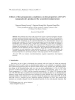
<i><b>Figure 1.1 Structure comparison between feedforward neural network (FNN, left) and </b></i>
<i>recurrent neural network (RNN, right). The yellow circles, blue circles and green circles represented input layer, hidden layer, and output layer, respectively. While FNN recommended to independent data, the output of RNN depend on the prior elements within the sequence, hence, the RNN has their distinct feedback connections in the hidden layer. </i>
The motivation for physical neural network implementation is to create fast information processing devices with low learning cost. We rely primarily on advanced material science for this physical implementation. ANNs models have recently been widely used in material science because of their unique features, which
</div><span class="text_page_counter">Trang 16</span><div class="page_container" data-page="16">allow them to be used as an alternative in electrical circuits with dynamic data processing [8]. Among the possible applications of various designs of material-based neural networks, reservoir computing (RC) is a promising route. RC is originally a recurrent neural network (RNN) based framework, therefore, it’s suitable for dynamic (temporal) information processing. As compared to conventional recurrent neural networks, RC offers the possibility of being able to learn quicker at a lower cost [9]. Its implementation based on an algorithm that learn data changes over time, input data are transformed into spatiotemporal pattern in a high-dimensional space by an RNN in the reservoir, then a pattern analysis from the spatiotemporal patterns is performed in the readout. The network nodes in the reservoir should change over time according to the input, as a result, the internal state of the reservoir is determined by both past and present inputs [10].
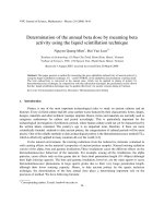
<i><b>Figure 1.2 RC framework where a reservoir for nonlinear mapping input into a </b></i>
<i>high-dimensional computational space (Left). The reservoir random network is unregulated and only the readout is trained by a simple supervised readout layer to learn the linear combinations of network states. Here, Ag/Ag<small>2</small>S aggregated NPs plays the role as reservoir layer by create a randomly connected network and combining with electrodes pattern to replicate RC system (Right). </i>
As illustrated in Figure 1.2, on the left side, a RC system consists of the input layer transmits time inputs, the reservoir, a nonlinear randomly connected network, for mapping input into a high-dimensional computational space, and the outputs layer is linked to a higher dimensional computational space. The reservoir random network is unregulated and only the readout is trained by a simple supervised readout layer to
</div><span class="text_page_counter">Trang 17</span><div class="page_container" data-page="17">optimizing the output weights and hence target task can be constructed just by performing a weighted linear combination of all the outputs. As a result, the main benefit of RC over other neural network methods is quick learning, which results in a lower training cost. Another benefit is that the dynamic behavior of reservoir random network may be advantageously implemented in hardware utilizing a variety of physical system in substrates and devices. For instances, RC could also be applied in a variety of physical systems such as photonic and memristive systems [11], thus, such physical reservoir computing is receiving increased attention in a variety of scientific areas. The physical realization of RC models has gained a lot of interest. Any system that is capable of exhibiting nonlinear dynamical responses has the potential to function as a reservoir [11]. A material-based reservoir must meet certain requirements in order to operate computing efficiently. Nonlinearity, phase shift and high dimensionality are three of these prerequisites [12]. When a RC system parameter variation causes a transition between non-chaotic and chaotic regimes, it is often recommended that the parameter be set close to the transition point (the so-called edge of chaos) where the transformation by a reservoir is neither very expanding nor very contracting [11]. This edge of chaos condition is crucial for all RC computing. However, because it is difficult to check in a material reservoir, these three properties are chosen instead of the edge of chaos. These electrical characteristics are needed for in-materio RC devices because they must demonstrate nonlinear sequential input into a high-dimensional computational space. The nonlinearity property enables reservoir to function as a nonlinear mapping, it is also essential for efficiently extracting nonlinear dependencies of input. High dimensionality is necessary to map input into high-dimensional space. The dimensionality related to the number of independent signals obtained from reservoir. This characteristic enables the extraction of input's spatiotemporal dependencies. Another essential property is phase shift, which represent for the influence of past inputs on current reservoirs state. This feature is especially crucial for describing sequential data with short-term memory.
</div><span class="text_page_counter">Trang 18</span><div class="page_container" data-page="18">1.1.3. Silver nanomaterials
In this nanoscale era, the advances in nanoscale technology are boosting a great impulse towards the miniaturization of device manufacturing, integration, and system design. Furthermore, nanoscale techniques have an enormous potential for developing novel materials and devices with distinct properties, balancing thermodynamic and kinetic effects. A hardware technique created employing nano-architectural approaches, provides a framework for the development of biologically inspired nanoscale logic and memory devices, known as the atomic switch [13]. The atomic switch is a memristive electro-ionic circuit element which provides multistate, nonlinear switching and synapse-like memory characteristics, operating through a bias-driven filamentary switching mechanism across a metal–insulator–metal junction [14]. A complex network comprised of nanomaterials (such as overlapping nanowire junctions [15] or aggregated nanoparticles [16]) enables the formation of a group of atomic switches. The distributed nonlinear dynamics of the atomic switching network (ASN) make it an ideal candidate for RC.
Considering their properties, noble metals such as silver nanomaterials are among the most intriguing elements. Recently, there has been a surge of interest in the study of the electrical characteristics of Ag/Ag<small>2</small>S, especially for its atomic switching network construction. Some Ag/Ag<small>2</small>S topologies and structures such as thin films [17] or nanowires [14] was investigated which manifesting atomic switching behavior, results in a consistent in I-V nonlinearity behavior and higher harmonics generation, exhibiting neuromorphic features. Such traits are projected to be improved by increasing relative surface area and built more interaction between the nanomaterials. Here, we investigated Ag/Ag<small>2</small>S nanoparticles (NPs) which has large surface area. In this study, the purpose is to investigate whether Ag/Ag<small>2</small>S aggregated NPs enable to play the role as reservoir layer by create a randomly connected network and combining with electrodes pattern to replicate RC system, as illustrated on the right side of Figure 1.2. Several investigations on nanomaterial-enabled RC computing in physical devices have been conducted, which are combined as references and
</div><span class="text_page_counter">Trang 19</span><div class="page_container" data-page="19">guidelines to inspire us to perform this work. Some representations were discussed in the following section.
<b>1.2. Literature survey: in-materio unconventional computing </b>
1.2.1. Atomic switch networks for reservoir computing
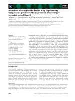
A next-generation computing system by ASN device which utilize Ag/Ag<small>2</small>S nanowire junction has been reported [15]. This ASN device contained 128 measurement electrodes, which is fabricated by using conventional lithographic methods by patterning platinum onto a thermally oxidized Si wafer followed by insulation with SU-8 and evaporated copper grid (Figure 1.3(a)). In the center, a complex network of overlapping silver nanowire junctions grown onto a multi-electrode array is functionalized to produce Ag∣Ag<small>2</small>S∣Ag atomic switches with controllable densities of up to 10<small>9</small> junctions/cm<small>2</small>, as shown in insect of Figure 1.3(b). The atomic switch operation is regulated by filament formation between silver nanowire junctions, result in this ASN device exhibit non-linear characteristics, validated for memristive activity, as depicted in Figure 1.3(b).
<i><b>Figure 1.3 (a) Next-generation atomic switching network (ASN) device structure comprise </b></i>
<i>of 128 lithographically patterned platinum measurement electrodes, insulating SU-8 dielectric layer point contacts and evaporated copper grid. (b) Memristive-like non-linear characteristics observed in single junctions of ASN device. Inset: enlarge view of silver nanowire junctions in the device center region. </i>
Utilizing the dynamic, non-linear guided by interacting atomic switches from silver
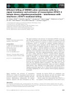
</div><span class="text_page_counter">Trang 20</span><div class="page_container" data-page="20">nanowire junctions, the ASN device was applied to the RC benchmark task of waveform generation. A 11 Hz bipolar sinusoidal voltage was injected to ASN for inducing switching activity, and the readout output was collected to optimized target wave forms: cosine, triangle, sawtooth square. The experimental accuracies in the 70–90% range were obtained, using 62 measurement electrodes, as shown in Figure 1.4.
<i><b>Figure 1.4 Result of RC benchmark task: waveform generation for ASN device with Ag/Ag</b><small>2</small>S nanowire junction. </i>
1.2.2. Gold nanoparticles network for reconfigurable Boolean logic
In an effort to realize unconventional computing in terms of materials engineering, a novel approach wherein new materials trained with new computational models can evolve as artificial intelligent systems to mimic logic gate functions. One such in-materio unconventional computing was studied in disordered Au nanoparticles, where the non-linear negative differential resistance output response was reconstructed to reconfigurable Boolean logic operations via real-time voltage optimizations with Evolutionary algorithm [16]. As shown in Figure 1.5 the device uses the nonlinear behavior generated by the interconnection of a disordered Au
</div><span class="text_page_counter">Trang 21</span><div class="page_container" data-page="21">nanoparticle network assembly in a 200 nm diameter circular area between the eight Ti/Au electrodes. At a low-temperature environment (≈ 0.3𝐾), the device exhibits Coulomb blockade and employs single-electron tunneling (SET) features. V<small>IN1</small> and V<small>IN2</small> are used as two electrodes input which introduced time-varying voltage signals. The other six electrodes are used to apply static control voltages V<small>1</small>–V<small>5</small> and measure the resultant current I<small>OUT</small>. A static voltage V<small>6</small> is also applied to the back gate. Based on the strongly nonlinear (switching) behavior of the SETs and their mutual interactions, these configuration voltages are repeatedly utilized to realize fully reconfigurable, robust Boolean logic in disordered Au NP networks.
<i><b>Figure 1.5 Schematic of disordered Au nanoparticles network reconfigurable Boolean logic. </b></i>
<i>The Au NPs, which are coupled by insulating molecules (1-octanethiols), are confined in a circular area (200 nm in diameter) constructed from 8 radial metal (Ti/Au) electrodes on top of a highly doped Si/SiO<small>2</small> substrate, which serves as a back gate. At low temperature (</i>≈
<i>0.3𝐾), as a result of the Coulomb oscillations of the individual NPs, this disordered NP </i>
<i>assembly generates an interconnected network of robust nonlinear periodic switches. These non-linear negative differential resistance output responses were reconstructed to reconfigurable Boolean logic operations via real-time voltage optimizations with Evolutionary algorithm.</i>
</div><span class="text_page_counter">Trang 22</span><div class="page_container" data-page="22">However, the drawback for this demonstration lay in the operating temperature condition is near-zero K, along with time inefficient training as each V parameter had to be trained individually. Therefore, in the field of material-based machine intelligence, what we desire for is a room temperature computation with straightforward and simultaneous parameter optimization model.
1.2.3. Spoken digit classification with silver iodide (AgI) nanowire networks.
Another investigation the ability of silver nanomaterials enables to realize physical
<i>RC was conducted by Sam Lilak et al [18]. An atomic switch networks comprising </i>
silver iodide (AgI) junctions has been physically characterized and utilized to classify spoken digit audio data. In this work, silver iodide was produced at ambient temperature by reaction of iodine vapor with silver nanowires in vapor phase. This material provides voltage-controlled resistance in both the bulk and when integrated into crossbar architectures, rendering it suitable as a memristive material for RC applications. As show in Figure 1.6, a 16-electrode grid of Pt was fabricated by photolithography, metal deposition and lift-off process, served as substrate for AgI ASN device enabling spatiotemporal stimulation and monitoring. AgI nanowire networks was tested for non-linear, temporal computation through the spoken digit classification.
</div><span class="text_page_counter">Trang 23</span><div class="page_container" data-page="23"><i><b>Figure 1.6 Schematic diagram of an AgI-based ASN device, from nanowire junction to chip. </b></i>
<i>(a) Filament formation process between two AgI nanowire junction. (b) Enlarge view of AgI nanowire network from scanning electron microscopy (SEM) image and optical image at the center of 16-electrode pattern. </i>
<i><b>Figure 1.7 (a) Flow chart for spoken digit recognition RC task using ASN-based devices </b></i>
<i>involved encoding and separation of raw audio data into frequency. Individual frequency was arranged to minimize input thrashing and then introduced as input voltage to the ASN device. Output data was collected from the rest electrodes. (b) Performance of the spoken digit classification task, as compared to using the “Input Only” mode, task performance was improved by the “Reservoir” readout method, as depicted via mean accuracy and standard deviation. Task performance still can be maintained under low-power operation of AgI ASNs. </i>
</div><span class="text_page_counter">Trang 24</span><div class="page_container" data-page="24">mel-AgI devices displayed distributed nonlinear dynamics over the whole nanowire network, resulting in a stable and repeatable nonlinear modification of the input signal. Based on these qualities, AgI nanowire networks were examined for spoken digit recognition RC task, as shown schematically in Figure 1.7(a). Firstly, raw audio data (spoken digit voice) were encoding and separation of into mel-frequency cepstrum coefficients (MFCCs). Individual MFCCs was arranged to minimize input thrashing and then introduced as input voltage to the ASN device. Output data was collected from the rest electrodes and optimized by linear regression. The result was depicted in Figure 1.7(b), the ASN reservoir demonstrated highly accurate, as compared to using the “Input Only” mode, task performance was improved by the “Reservoir” readout method, as depicted via mean accuracy and standard deviation. Task performance still can be maintained under low-power operation of AgI ASNs across a wide range of input voltages (0.5–10 V).
The novel AgI-based ASN devices described here acted as a dynamic, memristive reservoir for nonlinear temporal data processing and proved the potential to effectively classify spoken digits with high accuracy.
Combining all those preceding studies, these silver nanomaterial networks constitute both a promising material system ripe for further exploration and a possibility to advance the paradigm of in-materio RC computing forward practical applications. Hence, silver nanomaterials, particularly silver nanoparticles are considered as ideally research subjects in our study.
</div><span class="text_page_counter">Trang 25</span><div class="page_container" data-page="25"><b>1.3. Outline of research </b>
In the present study, we report the utilizing of Ag/Ag<small>2</small>S nanoparticles for developing material-based RC. The purpose is to investigate the possibility of using Ag/Ag<small>2</small>S nanoparticles to develop a new computing paradigm called in-materio reservoirs. Firstly, chapter one introduces the motivation, research field and literature survey to draw the objective and research scope for this study. Chapter two explains detail about synthesis material process, device fabrication and experiment set up for characterizing Ag/Ag<small>2</small>S NPs device.
Secondly, the characterization methods and working principle were investigated. The structural properties of Ag/Ag<small>2</small>S nanoparticles are confirmed by X-ray diffractometry (XRD) and transmission electron microscopy (TEM). Electrical characteristics are investigated via current-voltage (I-V) and voltage-time (V-t) measurement by using a Source Meter and a multifunctional data acquisition system. The characteristics requirements for building the in-materio physical reservoir computing, such as nonlinearity, high dimensionality, and phase shift have been investigated. These procedure and result depict in chapter three.
Lastly, after demonstrating that the Ag/Ag<small>2</small>S nanoparticle aggregates had the nonlinearity electrical behavior and additional characteristics required for RC hardware namely phase-shift and higher harmonics which are vital for the implementation of RC computing, in chapter four, RC benchmark task waveform generation is realized by a linear combination of outputs. Others more complicated RC task such as: objects classification, Boolean logic operations and spoken digit classification are also performed with microscale platinum electrodes to implement the nonlinear dynamics of Ag/Ag<small>2</small>S nanoparticles. Finally, chapter five presents the conclusion of this study along with some specific suggestions.
</div><span class="text_page_counter">Trang 26</span><div class="page_container" data-page="26"><b>CHAPTER 2 METHODOLOGY </b>
<b>2.1. Ag/Ag<small>2</small>S nanoparticles synthesis </b>The Ag/Ag<small>2</small>S nanoparticles were synthesized at room temperature by modified Schiffrin procedure [19] referring from earlier study of C. Battocchio et al [20]. As illustrated in Figure 2.1, experiment process is as follow: 200 mg silver nitrate (Signa-Aldrich, MW: 79.55 gr/mol) in deionized (DI) water was mixed with toluene solution of 360 mg tetraoctylammonium bromide (Signa-Aldrich, MW: 546.79 gr/mol), then 0.37 ml allyl mercaptan (Tokyo Chemical Industry, MW: 17.03 gr/mol) in toluene was added to the solution and left to react for 30 minutes while being stirred magnetically. Subsequently, a reducing agent of 260 mg sodium borohydride (Tokyo Chemical Industry, MW: 37.83 gr/mol) solution in DI water was added to the mixture and allowed to react for 2 hours under magnetically stirred. The water phase was then removed, and 250 ml ethanol was added to wash the excess of allyl mercaptan and toluene solution. The obtained solution then centrifugated at 4000 rpm for 20 minutes to separate the nanoparticles from the liquid phase. The Ag/Ag<small>2</small>S NPs was attained and ready to be used for further experiments.
<i><b>Brust-Figure 2.1 Ag/Ag</b><small>2</small>S NPs was synthesized following Brust-Schiffrin method. </i>
</div><span class="text_page_counter">Trang 27</span><div class="page_container" data-page="27"><b>2.2. Device fabrication </b>
For device realization, the optical lithography along with metal deposition was used to create the metal 16 electrodes. Firstly, electrodes pattern was designed by LayoutEditor software and used as the model for optical lithography. Next, SiO<small>2</small>/Si substrate was washed with acetone, immersed in isopropyl alcohol (IPA), washed again by DI water, each step takes 5 minutes, then dried with N<small>2</small> gas. Thereafter, 1 µm thickness of LOR-10 was put onto substrate using spin coater under 3000 rpm for 50 s, followed by heated it on hot place in 5 mins under 180 ℃. Then, 1.8 µm thin, homogenous layer of photosensitive resist is covered the substrate by sprinkling resist solution (S1818G filtered by 0.45 µm PTFE filter paper) onto the sample, which is then spun at 4000 rpm for 20 s. After baking the resist on hot plate (90 ℃, 5 mins), the sample is placed in a mask aligner, which is equipped with a high-powered light
<i>source performed by SUSS MicroTec photolithography machine, that exposes the </i>
resist film through the mask. By immersing the sample in developer MF-319 for 1 min, the corresponding parts of the resist film are removed, then rinse by DI water and dried with N<small>2</small> gas. The metallization step was done by depositing Pt/Ti (electrode material) with 24/6 nm of thickness on a SiO<small>2</small>/Si substrate, following metallization, the resist is typically removed by dimethyl-sulfoxide at 80 ℃ for 40 mins under sonicating in a lift-off process. There is a circular gap with 30 µm diameter in the central of electrodes array and the distance between two nearest electrodes is 4.5 µm. The 16 platinum electrodes pattern was archived and the RC in-materio reservoir device was formed by drop-casted 5 µL of the synthesized Ag/Ag<small>2</small>S NPs on the center of electrodes while putting on a hot plate set at 50 ℃ for ethanol solvent evaporation. A chip package was fabricated for the device, each electrode was connected to a pin, hence, multiples output electrodes could be recorded simultaneously to investigate the dynamic computing inside a reservoir. The device realization procedure was briefly illustrated in Figure 2.2.
</div><span class="text_page_counter">Trang 28</span><div class="page_container" data-page="28"><i><b>Figure 2.2. (a) The Ag/Ag</b><small>2</small>S NPs in-materio RC device realization by drop-casting those particles onto 16-electrodes produced by optical lithography, as a result the device was fabricated. The optical microscope image shows the center area enlarged view of electrodes pattern. There is a circular gap with 30 µm diameter in the central of electrodes array and the distance between two nearest electrodes is 4.5 µm. (b) A chip package was fabricated for the device with each electrode was connected to a pin for simultaneously measurement. </i>
</div><span class="text_page_counter">Trang 29</span><div class="page_container" data-page="29"><b>2.3. Characteristic measurement </b>
2.3.1. Structure characteristic measurement
To explore the characteristics of produced nanoparticles, a variety of characterization approaches were studied. X-ray diffraction spectrometry (XRD) and transmission electron microscopy (TEM) were used to investigate the structural properties of Ag/Ag<small>2</small>S NPs such as element identification, morphology, and particle size.
<i>2.3.1.1. X-ray diffraction spectrometer (XRD) </i>
X-ray diffraction (XRD) is a method for analyzing crystalline materials. Ag/Ag<small>2</small>S NPs sample preparing for XRD characterization is required in powder form. Following a successful synthesis as mentioned above, the Ag/Ag<small>2</small>S nanoparticle in ethanol solvent was collected and centrifuged, followed by a drying of the precipitates to get nanoparticle powder as show in Figure 2.3 (a). In this study, the sample was analysis using an X-ray diffractometer (Rigaku RINT-2100) with Cu Kα radiation at 40 kV (λ = 0.154 nm). The scan rate was 0.02 degrees per second. This method's operating process relies on an emitted X-ray beam with a λ wavelength that assails lattice structure in a crystal plane at an θ angle. The result for XRD characterization will be shown in section 3.1.1.
<i><b>Figure 2.3. (a) The sample holder covered by Ag/Ag</b><small>2</small>S powder prepared for X-ray diffraction (XRD) analysis process. (b) X-ray diffractometer (Rigaku RINT-2100) picture.</i>
</div><span class="text_page_counter">Trang 30</span><div class="page_container" data-page="30"><i>2.3.1.2. Transmission electron microscopy (TEM) </i>
Transmission electron microscopy (TEM) is a method for examining the characteristics of extremely tiny objects particularly in nanoscale. In this study, transmission electron microscopy (TEM, JEOL-2100) with acceleration voltage at 200 kV was utilized for morphology analysis of Ag/Ag<small>2</small>S nanoparticles. Because the wavelength of an electron is substantially short, TEM was used to examine particles at much higher magnification and resolution. Compared to scanning electron microscope, which can only scan and observed the sample's surface, TEM also produces better resolution pictures. From TEM image the morphology of nanoparticles is able to observe, and the particles diameter can be calculated. Sample preparation for TEM is also simple, there is a sample holder have grid shape and the Ag/Ag<small>2</small>S NPs in ethanol solvent was drop into the grid then get it dry by using hot plate at 50 ℃, the sample holder image and sample preparation are briefly illustrated in Figure 2.4. This is how TEM operate: a beam of electrons is fired by an electron gun. Using extreme high-level voltages of up to several million volts, electrons were accelerated to exceedingly high speeds. The vacuum system is required to ensure the acceleration process. Then, a condenser lens focuses the electron beam into a narrow beam. Electrons pass through the ultra-thin specimen and depending on the transparent degree of the sample to electrons, some components of the beam are transmitted. The objective lens converts the sample's output beam into a picture. The TEM analysis result will be shown in section 3.1.2.
<i><b>Figure 2.4. Transmission electron microscopy (TEM) sample preparation and TEM sample </b></i>
<i>grid holder structure. </i>
</div><span class="text_page_counter">Trang 31</span><div class="page_container" data-page="31">2.3.2. Electrical characteristic measurement
The purpose of fabricating the device is to investigate the possibility of Ag/Ag<small>2</small>S nanoparticles to be used as an in-materio reservoir computing hard-ware. Therefore, the required electrical property of RC devices must appear on this Ag/Ag<small>2</small>S NPs device. Several characterization techniques, including current-voltage (I-V) characteristics and RC characterize measurement, were used to explore the electrical properties of the Ag/Ag<small>2</small>S nanoparticles-based device.
<i>2.3.2.1. Current-voltage measurement </i>
Current-voltage measurement was carried out by using a Source Meter (Keithley 2400). The experiment set up was shown in Figure 2.5, the Ag/Ag<small>2</small>S NPs device was connected to probe via a Source Meter, to extract the electrical responses a bias 0 V to 4 V with 0.02 V step voltage in 1000 milliseconds time step was repeatedly applied sweeping of forward and reversed to the device, a 1 mA compliance current was set at to prevent the device damage. A PC wired to Source Meter with LabView software functionalized to control the measurement procedure. The I-V data were recorded at ambient temperature.
<i><b>Figure 2.5. Current-voltage measurement set up by using a Source Meter (Keithley 2400). </b></i>
<i>The experiment was carried out under room temperature.</i>
</div><span class="text_page_counter">Trang 32</span><div class="page_container" data-page="32"><i>2.3.2.2. RC characterize measurement. </i>
Time series data is the most commonly used sort of data for RC tasks. Exploiting the material network's dynamics is critical for RC to be efficiently trained to perform a given task. Therefore, it is essential to build up a measuring system that enable to record multiple output signals from different points of the Ag/Ag<small>2</small>S network over time to be used as the reservoir states. The Ag/Ag<small>2</small>S NPs device was connected to a measuring system that was set up to execute the RC characterization and RC tasks indicated in Figure 2.6. The input signal caused the dynamics of the Ag/Ag<small>2</small>S network is fed through a signal generating device (which can generate the desired input data). Subsequently, the multifunction data acquisition DAQ (National Instruments PXIe-6363) system measures and reads output signals gathered simultaneously from multiple electrode pads of the device design. Multifunction DAQ’s wires link the electrode to the electrical probes. To monitor the I/O signals, the PC plays the role as a software interface between the signal generating device and the DAQ using the LabVIEW program.
<i><b>Figure 2.6. Schematic of an electrical measurement setup used for obtaining the dynamic </b></i>
<i>outputs for constructing the RC characterization and carrying out RC task.The Ag/Ag<small>2</small>S reservoir device receives an input signal from the signal generating device via the input electrical probe, and the corresponding individual outputs from the device's numerous electrodes are read by the DAQ via the output electrical probe and the PC using LabVIEW for software optimization.</i>
</div><span class="text_page_counter">Trang 33</span><div class="page_container" data-page="33"><b>CHAPTER 3 DEVICE CHARACTERIZATION </b>
<b>3.1. Structural properties </b>3.1.1. X-ray diffraction spectrometer (XRD) result
For element identification for obtained nanoparticles, X-ray diffractometry (XRD, Rigaku RNIT-2100) with Cu Kα radiation 40kV (λ = 0.154 nm) and scanning rate was 0.02 °/s was performed. Figure 3.1 show the XRD profiles of the synthesized nanoparticles with the inset is enlarged view for the Ag<small>2</small>S peaks area indicated by blue squares which is overwhelmed by Ag peaks intensity indicated by orange circles. The Ag and Ag<small>2</small>S phase in XRD result was matched with the references of PDF No: 01-071-3762 Quality: I [21] and PDF No: 01-075-1061 Quality: B [22], respectively. As shown in the XRD profile, these two substances were assigned to the acquired peaks, and it was proven that the Ag<small>2</small>S phase and the Ag phase coexistence in the produced nanoparticles.
<i><b>Figure 3.1 Synthesized Ag/Ag</b><small>2</small>S NPs structure characteristics. X-ray diffractometry (XRD) pattern for archived nanoparticles sample, the obtained peaks were attributed to Ag and Ag<small>2</small>S peaks, and it was confirmed that these two substances coexistence in the produced nanoparticles. </i>
</div><span class="text_page_counter">Trang 34</span><div class="page_container" data-page="34">3.1.2 Transmission electron microscopy (TEM) result
The morphology of Ag/Ag<small>2</small>S nanoparticles were confirmed by transmission electron microscopy (TEM, JEOL-2100) with acceleration voltage at 200 kV. As shown in Figure 3.2(a), nanoparticles have spherical forms, the average particle sizes were estimated by calculating the diameter from measuring the area of nanoparticles from TEM images using Image J software. To determine the average diameter of nanoparticles, a Gaussian curve was fitted to the histogram of particle size distribution obtained from TEM image analysis, the average diameter was specified around 31.37 nm, which is depicted in Figure 3.2(b)
<i><b>Figure 3.2 (a) Transmission electron microscopy (TEM) image of Ag/Ag</b><small>2</small>S NPs with 100 nm scale bar. (b) The distribution of the diameters of particles calculated from TEM image, the average diameter of synthesized sample was extracted by fitting with Gaussian curve for histogram of particles size distribution. The average of particles diameter approximate 31.37 nm with standard deviation is around 15.53. </i>
<b>3.2. Electrical properties </b>
3.2.1. Current-voltage characteristic result (Non-linearity behavior)
To investigate the electrical properties, current-voltage measurement was carried out by using a Source Meter (Keithley 2400). The repeated sweeping of forward and reversed bias 0 V to 4 V with step voltage 0.02 V each one second was applied to the
</div><span class="text_page_counter">Trang 35</span><div class="page_container" data-page="35">device, the compliance current was set at 1 mA to prevent the device damage. As depicted in Figure 3.3(a) an intensely nonlinear response and a gradually increase in the output current were observed. In the first sweep, the current began to raise at 3 V and reached 0.5 mA, allowing the development of certain silver filaments among the nanoparticles. During the first sweep's reverse bias, the output current displayed nonlinear response with the curve of forward sweep and the current slowly decreased, representing filament disintegration. Following that, in the second sweep, the output current began to rise at an applied bias voltage of around 0.8 V, which was lower than the first sweep. Furthermore, considerable current variations occurred in the 2V to 4V range, indicating the production and destruction process of conduction paths proceeded randomly at various gap sites among NPs. A sufficient potential applied across the nanoparticles is the source for the production and destruction of silver filament between the particles. When the bias voltage was connected to the system, an amount of charging electrons was introduced into the device, initiating the redox reaction process at the surface of Ag/Ag<small>2</small>S nanoparticles [23]. The gap between each nanoparticle was created by Ag<small>2</small>S and the organic layer, after the voltage was applied, Ag nanoparticles oxidized the electrode, Ag<small>+</small> ions were reduced by the electron injected, silver metallic bridges were generated by the breakage of the insulating layer, and the conduction paths was formed among the nanoparticles. Additional bias sweep results in the gradually increase of the output current up to reach the compliance current 1 mA, indicating a strong connection was generated in the Ag/Ag<small>2</small>S nanoparticles network, as shown in the third sweeping voltage.
</div>