Optical Networks: A Practical Perspective - Part 67 pdf
Bạn đang xem bản rút gọn của tài liệu. Xem và tải ngay bản đầy đủ của tài liệu tại đây (730.78 KB, 10 trang )
630 PHOTONIC PACKET SWITCHING
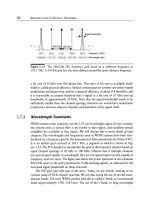
Figure
12.10 Block diagram of a soliton-trapping logical AND gate.
Figure
12.11 Illustration of the operation of a soliton-trapping logical AND gate. (a)
Only one pulse is present, and very little energy passes through to the filter output. This
state corresponds to a logical zero. (b) Both pulses are present, undergo wavelength shifts
due to the soliton-trapping phenomenon, and most of the energy from one pulse passes
through to the filter output. This state corresponds to a logical one.
will not be selected by the filter. Thus the filter output has a pulse (logical one) only
if both pulses are present at the input, and no pulse (logical zero) otherwise.
12.2 Synchronization 631
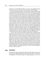
Figure
12.12 The function of a synchronizer. (a) The two periodic pulse streams with
period T are out of synchronization; the top stream is ahead by AT. (b) The two periodic
streams have been synchronized by introducing a delay AT in the top stream relative to
the bottom stream.
12.2
Synchronization
Synchronization
is the process of aligning two pulse streams in time. In PPS networks,
it can refer either to the alignment of an incoming pulse stream and a locally available
clock
pulse stream or to the relative alignment of two incoming pulse streams. Recall
our assumption of fixed-size packets. Thus if framing pulses are used to mark the
packet boundaries, the framing pulses must occur periodically.
The function of a synchronizer can be understood from Figure 12.12. The two
periodic pulse streams, with period T, shown in Figure 12.12(a) are not synchronized
because the top stream is ahead in time by AT. In Figure 12.12(b), the two pulse
streams are synchronized. Thus, to achieve synchronization, the top stream must be
delayed by AT with respect to the bottom stream. The delays we have hitherto con-
sidered, for example, while studying optical multiplexers and demultiplexers, have
been
fixed
delays. A fixed delay can be achieved by using a fiber of the appropriate
length. However, in the case of a synchronizer, and in some other applications in
photonic packet-switching networks, a
tunable delay
element is required since the
amount of delay that has to be introduced is not known a priori. Thus we will now
study how tunable optical delays can be realized.
632
PHOTONIC PACKET SWITCHING
c 1 Delay
C 2
Delay
Ck-
2 Delay
ck- 1
Delay c k
T/2 k- 2 T/2 k- 1
,.12•215
ooo ,.
Input switch~ ___~switchl Delayed
pulse ] ~176176 pulse
stream stream
~ ooo ~ ~
Stage 1 Stage k- 2
r
Stage k- 1
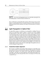
Figure 12.13 A tunable delay line capable of realizing any delay from 0 to
T - T/2 k-1
in steps of
T/2 k-1.
12.2.1
Tunable Delays
A tunable optical delay line capable of realizing any delay, in excess of a reference
delay, from 0 to
T- T/2 k-l,
in steps of
T/2 k-l,
is shown in Figure 12.13. The
parameter k controls the resolution of the delay achievable. The delay line consists
of k- 1 fixed delays with values
T/2, T/4 T/2 k-1
interconnected by k 2 • 2
optical switches, as shown. By appropriately setting the switches in the cross or
bar state, an input pulse stream can be made to encounter or avoid each of these
fixed delays. If all the fixed delays are encountered, the total delay suffered by the
input pulse stream is
T/2 + T/4 + + T/2 k-1 = T - T/2 k-1.
This structure can
be viewed as consisting of k - 1 stages followed by an output switch, as indicated
in Figure 12.13. The output switch is used to ensure that the output pulse stream
always exits the same output of this switch. The derivation of the control inputs
Cl, c2 Ck
to the k switches is discussed in Problem 12.3.
With a tunable delay line like the one shown in Figure 12.13, two pulse streams
can be synchronized to within a time interval of
T/2 k.
The value k, and thus the
number of fixed delays and optical switches, must be chosen such that
2-kT
<< r,
the pulse width. The resolution of the delay line is determined by the speed of the
switches used and the precision to which the delay lines can be realized. Practically,
the resolution of this approach may be on the order of 1 ns or so. We can use
this approach to provide
coarse
synchronization. We will also need to perform
fine
synchronization to align bits to within a small fraction of a bit interval. One approach
is to use a tunable wavelength converter followed by a highly dispersive fiber line
[Bur94]. If D denotes the dispersion of the fiber used, A)~ the output wavelength
range, and L the length of the fiber, then we can get a relative delay variation of 0
to
DA~.L.
If the output wavelength can be controlled in steps of 3)~, then the delay
resolution is
D3)~L.
12.2 Synchronization
633
Given a tunable delay, the synchronization problem reduces to one of determining
the relative delay, or
phase,
between two pulse streams. A straightforward approach
to this problem is to compare all shifted versions of one stream with respect to the
other. The comparison can be performed by means of a logical AND operation.
This is a somewhat expensive approach. An alternative approach is to use an optical
phase lock loop
to sense the relative delay between the two pulse streams. Just as
more than one phenomenon can be used to build an optical AND gate, different
mechanisms can be used to develop an optical phase lock loop. We discuss one such
mechanism that is based on the NOLM that we studied in Section 12.1.3.
12.2.2
Optical Phase Lock Loop
Consider an NOLM that does not use a separate nonlinear element but rather uses
the intensity-dependent refractive index of silica fiber itself as the nonlinearity. Thus
if a low-power pulse stream, say, stream 1, is injected into the loop~from arm A of
the directional coupler in Figure 12.8(a)~the fiber nonlinearity is not excited, and
both the clockwise and the counterclockwise propagating pulses undergo the same
phase shift in traversing the loop. As a consequence, no power emerges from the
output (arm B) in this case. If a high-power pulse stream, say, stream 2, is injected
in
phase
(no relative delay) with, say, the clockwise propagating pulse stream, because
of the intensity dependence of the refractive index of silica fiber, the refractive index
seen by the clockwise pulse, and hence the phase shift undergone by it, is different
from that of the counterclockwise pulse. This mismatch in the phase shift causes an
output to emerge from arm B in Figure 12.8(a). Note that if the high-power pulse
stream is not in phase (has a nonzero relative delay) with the clockwise propagating
pulse stream, the clockwise and counterclockwise pulses undergo the same phase
shift, and no output emerges from arm B of the directional coupler. To achieve
synchronization between pulse streams 1 and 2, a tunable delay element can be used
to adjust their relative delays till there is no output of stream 1 from the NOLM.
Note that the same problem of discriminating between the pulse streams 1 and
2 at the output of the directional coupler (arm B) as with the TOAD arises in
this case as well. Since pulses from stream 2 will always be present at the output,
in order to detect the absence of pulses from stream 1, the two streams must use
different wavelengths or polarizations. When different wavelengths are used, because
of the chromatic dispersion of the fiber, the two pulses will tend to walk away from
each other, and the effect of the nonlinearity (intensity-dependent refractive index)
will be reduced. To overcome this effect, the two wavelengths can be chosen to lie
symmetrically on either side of the zero-dispersion wavelength of the fiber so that
the group velocities of the two pulse streams are equal.
634 PHOTONIC PACKET SWITCHING
A phase lock loop can also be used to adjust the
frequency and phase
of a local
clock source~a mode-locked laser~to those of an incoming periodic stream. We
have seen in Section 3.5.1 that the repetition rate, or frequency, of a mode-locked
laser can be determined by modulating the gain of the laser cavity. We assume that
the modulation frequency of its gain medium, and hence the repetition rate of the
pulses, is governed by the frequency of an electrical oscillator. The output of the
NOLM can then be photodetected and used to control the frequency and phase of
this electrical oscillator so that the pulses generated by the local mode-locked laser
are at the same frequency and phase as that of the incoming pulse stream. We refer
to [Bar96] and the references therein for the details.
Another synchronization function has to do with extracting the clock for the
purposes of reading parts of the packet, such as the header, or for demultiplexing the
data stream. This function can also be performed using an optical phase-locked loop.
However, this function can also be performed by sending the clock along with the
data in the packet. In one example [BFP93], the clock is sent at the beginning of the
packet. At the switching node, the clock is separated from the rest of the packet by
using a switch to read the incoming stream for a prespecified duration corresponding
to the duration of the clock signal. This clock can then be used to either read parts
of the packet or to demultiplex the data stream.
12.3
Header Processing
For a header of fixed size, the time taken for demultiplexing and processing the
header is fixed, and the remainder of the packet is buffered optically using a delay
line of appropriate length. The processing of the header bits may be done electron-
ically or optically, depending on the kind of control input required by the switch.
Electrically controlled switches employing the electro-optic effect and fabricated in
lithium niobate (see Section 3.7) are most commonly used in switch-based network
experiments today. In this case, the header processing can be carried out electron-
ically (after the header bits have been demultiplexed into a parallel stream). The
packet destination information from the header is used to determine the outgoing
link from the switch for this packet, using a look-up table. For each input packet,
the look-up table determines the correct switch setting, so that the packet is routed
to the correct output port. Of course, this leads to a conflict if multiple inputs have a
packet destined for the same output at the same time. This is one of the reasons for
having buffers in the routing node, as explained next.
If the destination address is carried in the packet header, it can be read by
demultiplexing the header bits using a bank of AND gates, for example, TOADs,
as shown in Figure 12.7. However, this is a relatively expensive way of reading
12.4 Buffering
635
the header, which is a task that is easier done with electronics than with optics.
Another reason for using electronics to perform this function is that the routing and
forwarding functions required can be fairly complex, involving sophisticated control
algorithms and look-up tables.
With this in mind, several techniques have been proposed to simplify the task
of header recognition. One common technique is to transmit the header at a much
lower bit rate than the packet itself, allowing the header to be received and processed
relatively easily within the routing node. The packet header could also be transmitted
on a wavelength that is different from the packet data. It could also be transmitted on
a separate subcarrier channel on the same wavelength. All these methods allow the
header to be carried at a lower bit rate than the high-speed data in the packet, allow-
ing for easier header processing. However, given the high payload speeds involved
in order to maintain reasonable bandwidth utilization without making the packet
size unreasonably large, we will have to use fairly short headers and process them
very quickly this may not leave much room for sophisticated header processing.
See Problem 12.5 for an example.
12.4
Buffering
In general, a routing node contains buffers to store the packets from the incoming
links before they can be transmitted or forwarded on the outgoing links. Hence the
name
store and forward
for these networks. In a general store-and-forward network,
electronic or optical, the buffers may be present at the inputs only, at the outputs
only, or at both the inputs and the outputs, as shown in Figure 12.2. The buffers may
also be integrated within the switch itself in the form of random access memory and
shared among all the ports. This option is used quite often in the case of electronic
networks where both the memory and switch fabric are fabricated on the same
substrate, say, a silicon-integrated circuit, but we will see that it is not an option for
optical packet switches. We will also see that most optical switch proposals do not
use input buffering for performance-related reasons.
There are at least three reasons for having to store or buffer a packet before it
is forwarded on its outgoing link. First, the incoming packet must be buffered while
the packet header is processed to determine how the packet must be routed. This
is usually a fixed delay that can be implemented in a simple fashion. Second, the
required switch input and/or output port may not be free, causing the packet to be
queued at its input buffer. The switch input may not be free because other packets
that arrived on the same link have to be served earlier. The switch output port may
not be free because packets from other input ports are being switched to it. Third,
after the packet has been switched to the required output port, the outgoing link
636 PHOTONIC PACKET SWITCHING
i
switchl ~lswitchl ~lswitc~
"1 I "1 I "7 I :
"
Figure 12.14
tecture.
Example of a 2 x 2 routing node using a feed-forward delay line archi-
from this port may be busy transmitting other packets, thus making this packet wait
for its turn. The latter delays are variable and are implemented differently from the
fixed delay required for header processing.
The lack of good buffering methods in the optical domain is a major impediment.
Unlike the electronic domain, we do not have random access memory in the optical
domain. Instead the only way of realizing optical buffers is to use fiber delay lines,
which consist of relatively long lengths of fiber. For example, about 200 m of fiber
is required for 1 #s of delay, which would be sufficient to store 10 packets, each
with 1000 bits at 10 Gb/s. Thus usually very small buffers are used in photonic
packet-switching networks. Note that unlike an electronic buffer, a packet cannot
be accessed at an arbitrary point of time; it can exit the buffer only after a fixed
time interval after entering it. This is the time taken for the packet to traverse the
fiber length. This constraint must be incorporated into the design of PPS networks.
Of course, by repeated traversals of the same piece of fiber, packet delays that are
multiples of this basic delay can be obtained.
PPS networks typically make use of delay lines in one of two types of con-
figurations. Figure 12.14 shows one example of a
feed-forward
architecture. In
this configuration, a two-input, two-output routing node is constructed using three
2 x 2 switches interconnected by two delay lines. If each delay line can store one
packet that is, the propagation time through the delay line is equal to one slot the
routing node has a buffering capacity of two packets. If packets destined for the same
output arrive simultaneously at both inputs, one packet will be routed to its correct
output, and the other packet will be stored in delay line 1. This can be accomplished
by setting switch 1 in the appropriate state. This packet then has the opportunity to
be routed to its desired output in a subsequent slot. For example, if no packets arrive
in the next slot, this stored packet can be routed to its desired output in the next slot
by setting switches 2 and 3 appropriately.
The other configuration is the
feedback
configuration, where the delay lines
connect the output of the switch back to its input. We will study this configuration
in Section 12.4.3.
12.4 Buffering
637
There are several options for dealing with contention resolution in an optical
switch. The first option is to provide sufficient buffering in the switch to be able
to handle these contentions. We will see in order to achieve reasonable packet loss
probabilities, the buffers need to be able to accommodate several hundred pack-
ets. As we have seen above, this is not a trivial task in the context of optical
buffers.
Another option is to drop packets whenever we have contentions. This is not
attractive because such events will occur quite often unless the links are occupied by
very few packets compared to their capacities. For each such event, the source must
retransmit the packet, causing the effective link utilization to drop even farther.
A third option is to use the wavelength domain to help resolve conflicts. This can
help reduce the amount of buffering required in a significant way.
The final option is for the packet to be
misrouted
by the switch, that is, transferred
by the switch to the
wrong output.
This option, termed
deflection routing,
has
received considerable study in the research literature on PPS networks.
We start by describing the various types of buffering, and the use of the wave-
length domain to resolve conflicts, followed by deflection routing. The switch
architectures used in the following section are idealized versions for illustration
only; we will look at some actual proposals and experimental configurations in
Section 12.6.
12.4.1
Output Buffering
Consider the switch with output buffering shown in Figure 12.15. Let us assume that
time is divided into slots and packets arriving into the switch are aligned with respect
to these time slots. In each time slot, we have packets arriving at the input ports. Of
these, one or more packets may have to be switched to the same output port. In the
worst case, we could have a packet arriving at each input port, with all these packets
destined to a single output port. In this case, if the switch is designed to operate at N
times the line rate (N being the number of ports), these packets can all be switched
onto the output port. However, only one of these packets can be transmitted out
during this time slot, and the other packets will have to stored in the output buffer.
If the output buffer is full, then packets will have to be dropped. The packet loss
probability indicates how frequently packets are dropped by the switch. For each
such event, the source must retransmit the packet causing the effective link utilization
to drop even farther. We can minimize the packet loss probability by increasing the
buffer size. With sufficiently large output buffers, an output-buffered switch has the
best possible performance with respect to packet delay and throughput, compared
to other switch architectures. The throughput can be viewed as the asymptotic value
638
PHOTONIC PACKET SWITCHING
Figure
12.15 A generic switch with output buffers.
of the offered load at which the packet delay through the switch becomes very large
(tends to infinity).
We can use a simple model to understand the performance of the different buffer-
ing techniques. The model assumes that in each time slot, a packet is received at the
input with probability p. Thus p denotes the traffic load. It further assumes that
traffic is uniformly distributed, and therefore the packet is destined to a particular
output port with probability
1/N,
where N is the number of ports on the switch.
While this is admittedly not a very realistic model, it gives some understanding of
the trade-offs between the different buffering approaches. The parameters of interest
are the desired packet loss probability, the number of packet buffers needed, and
the traffic load. The number of packet buffers suggested by this model is typically
smaller than what is actually required, since in reality traffic is more bursty than
what is assumed by this model.
For the output-buffered switch, this simple model was analyzed in [HK88], which
shows that to get a packet loss of
10 -6 at
a traffic load of 0.8, we need about 25
packet buffers per output. With sufficiently large buffers, a throughput close to 1
can be obtained.
One issue with the output-buffered switch is that the switch needs to operate at
N times the line rate per port. That is, it needs to be able to switch up to N packets
per time slot from different inputs onto the same output. This is quite difficult to
implement with optical switches. For this reason, many optical switch proposals
emulate an output-buffered switch while still operating at the line rate per port. If
multiple packets arriving in a time slot are all destined to the same output port, the
switch schedules different delays for each of these packets at the input so that they
get switched to the output in different succeeding time slots. For example, the switch
handles the first packet immediately, delays the next packet by one time slot at the
input, delays the next by two slots, and so on.
12.4 Buffering
639
Figure 12.16 Head-of-line blocking in an input-buffered switch. Observe that the
packet destined for output 1 in input buffer 2 is blocked despite the fact that the output
is free.
12.4.2
12.4.3
Input Buffering
A switch with input buffering has buffers at the input to the switch but not at the
output. These switches have relatively poor throughput due to a phenomenon called
head-of-line
(HOL) blocking, which is illustrated in Figure 12.16. When we have
multiple input packets at the head of the line destined to a single output port, only
one packet can be switched through. The other packets, however, may block packets
behind them from being switched in the same time slot. For example, in Figure
12.16, we have packets at port 1 and port 2 at the head of their lines, both destined
for port 3. Say we switch the packet at port 1 onto port 3. The second packet in
line behind the head-of-line packet on port 2 is destined to output port 1 but cannot
be switched to that output, even though it is free. For the traffic model considered
earlier, this HOL blocking reduces the achievable throughput to 0.58 for large switch
sizes [HK88]. While we can improve the throughput by selecting packets other than
just the one at the head of the line, this is quite complicated and not feasible in
the context of optical switches. The other problem is that the packet's delay at the
input buffer cannot be determined before placing the packet in the buffer because it
depends on the other inputs. In the context of optical delay lines, it means that when
the packet exits the delay line, we may still not be able to switch it through as the
desired output may be busy. For these reasons, optical switches with input buffers
only are not a good choice.
Recirculation Buffering
In this approach, the buffers connect the outputs back to the inputs. Typically, some
of the switch ports are reserved for buffering only, and the output of these ports is
connected back to the corresponding inputs via buffers. If multiple packets destined