Fiber Optics Illustrated Dictionary - Part 75 potx
Bạn đang xem bản rút gọn của tài liệu. Xem và tải ngay bản đầy đủ của tài liệu tại đây (1.04 MB, 10 trang )
Fiber
Optics
Illustrated
Dictionary
away
at
full
speed.)
2.
The
tendency
to
continue
a
sig-
nal,
echo,
electrical
charge,
or
data
transmission
af-
ter
the
actual
communication
has
ceased
or
the
mes-
sage part
has
been
received.
3.In aphosphor display
system,
the
tendency
of
the
phosphors
to
continue
to
fluoresce
after
the
stimulus
has
stopped.
This
may
be
an
undesired
property,
causing
smear,
or
may
be
a
de-
sired
property,
enabling
the
image
to
remain
view-
able
while
the
rest of
the
frame
is
being
imaged.
persistence of
vision
A
phrase
that
describes
the
way
in
which
human
visual
perception "holds"
an
image
for
a brief
moment,
about
a
tenth
ofa
second,
even
if
the
objects
in
the
visual
field
have
changed
or
moved.
Thus,
humans
can
only
scan
or
perceive still
images
up
to
a
speed
of
about
24
to
60
frames
per
second.
Faster
than
that
and
they
are
no
longer
seen
as
still
images,
but
as
a
series
of
moving
or related
images,
especially if
the
forms
in
the
images
are
closely
re-
lated
to
the
previous
ones.
Researchers
Muensterberg
and
Wertheimer
demonstrated
in
the
early
1900s
that
this
was
a
property
of
brain
processing
and
percep-
tion
more
than
a
physical
property
of
the
retina.
These
characteristics of
visual
perception
have
greatly
in-
fluenced
the
design
and
development of
moving
vi-
sual
communications
technologies.
See
frame,
scan
lines.
Personal
Communication
Network
PCN.
See
Glo-
bal
System
for
Mobile
Communications
for
the
back-
ground
and
technology
base
for
PCN.
PCN
was
de-
veloped,
starting
in
the
late
1
980s,
as
a
modified
form
ofGSM
operating
in
the
1800-MHz
frequency
band
(GSM
is
900
MHz).
It
has
smaller
cell
sizes, requires
lower
power,
and
is
optirnized
to
handle
higher
den-
sity
traffic
than
GSM,
but
otherwise
is
essentially
the
same.
The
PCN
standard
was
finalized
in
1991.
It
is
primarily
used
in
the
United
Kingdom.
See
Global
System
for
Mobile
Communications.
Personal Communications Service.
PCS.
A
low-
power,
higher
frequency,
standards-based, wireless
mobile communications system, operating
in
the
1800-
and
I900-MHz
range,
implemented
in
the
mid-
1990s.
Most
PCS
systems
are
100%
digital.
In
con-
trast
to
cellular,
which
is
limited
to
A
and
B carriers,
PCS
operates
across
six
(A
to
F)
carriers.
In
other
words,
cellular
can
be
thought
of
as
a subset of
PCS
in
its
broadest
sense.
Three
operational categories of
PCS
have
been
de-
fined
by
the
Federal Communication Commission
(FCC)
as
shown
in
the
PCS
Categories chart.
In
PCS,
particular
channels
are
assigned
to
specific
cells,
with
provision
for
reuse.
A
channel
is
associ-
ated
with
one
uplink
and
one
downlink
frequency.
A
specific number
of
channels
is
assigned
to
an
operator's
authorized
frequency
block.
PCS
service
can
be
installed
as
a centralized
or
distributed
archi-
tecture,
and
supports
both
time
and
code division
multiple
access (TDMA, CDMA). Designed
to
broaden
market
distribution ofwireless services,
the
system
may
have
more
limited
range
than
traditional
cellular,
but
the
cheaper
connect
times
and
handsets
may
be
appealing
to
consumers.
Industry
watchers
are
predicting
steady
growth
in
mobile
communications.
732
In
Japan
alone,
there
were
more
than
20
million
In-
ternet-capable
PCS
system
subscribers
by
200
I.
See
AMPS,
cellular
phone,
DAMPS,
DCS,
GSM,
Per-
sonal
HandyPhone
Service.
PCS Categories
Category Notes
narrowband
PCS
PCS
operating
in
limited
bandwidth
in
the
900-MHz
spectrum
and
not
suited
to
high
speed
data
communications,
although
low-bandwidth
short
text
messages
would
work.
Best
suited
to
in-building
and
near
outside-premises
use,
pagers,
and
cordless
phones.
broadband PCS
PCS
in
the
1.9-GHz
spectrum
range
for
better
quality
voice
communications
and
higher
duplex-mode
data
communications.
unlicensed PCS
PCS
in
the
1910-
to
1930-
MHz
range,
suitable
for
in-
house
and
in-company
systems,
and
small
independent
service
providers.
Limited
to
low-power
signals.
personal computer Pc. A
compact,
relatively
low-
cost computer system designed
for
home,
school,
small
business,
and
prosumer (high-end consumer)
use.
The
first
fully
assembled,
affordable
PC
with a
keyboard and
CRT
monitor was probably the
SPHERE
computer
released
in
1975,
but
it
didn't
sell
well.
Subsequently,
the
Radio
Shack
TRS-80
series,
followed closely
by
the
Apple computers
and
the
Commodore
PET
were
all
commercially successful.
At
the
time
of
the
introduction ofpersonal comput-
ers
in
the
mid-
and
late-I
970s,
the
cost
ofa worksta-
tion-level computer
was
typically
$40,000
and
more,
so
the
price
tag
of
about
$2000
to
$6000
for
a per-
sonal
computer with useful peripherals (printer,
mo-
dem,
etc.)
was
revolutionary
in
terms
of
availability
to
individuals.
In
the
early
1980s,
when
networks
that
could
interconnect individual
PCs
began
to
prolifer-
ate
and
CPUs
became
more
powerful,
the
distinction
between
personal
computers
and
higher
end
systems
began
to
blur - a progression
that
continues
to
this
day,
with
personal
computers
of
the
1990s
being
more
powerful
than
minicomputers a
decade
earlier
and
laptop
computers of
the
2000s
being
more
powerful
than
mid-range
institutional
computing
systems
of
the
late
1980s.
The
development of
PC
networks also
opened
up
hybrid
systems,
with
PCs
sharing
the
com-
puting
power of mainframes
and
mainframes
using
PCs
as
1/0 devices.
© 2003 by CRC Press LLC
The
tenn
PC
has
been
generically
applied
to
systems
used
by
individuals
for
personal, educational,
and
business
purposes,
and
so
does
not
fit
the
tenn "per-
sonal"
in
its
strictest
sense.
Some
people
use
PC
to
refer
only
to
ffiM-compatibles,
which
is
not
really
a
correct
l1se
of
the
tenn
and
has
probably
proliferated
because
"ffiM-compatible"
is
such
a
mouthful.
The
distinction
between
a
PC
and
a
workstation
is
not
as
cut-and-dried
as
many
people
think.
By
the
time
you
add
a
graphics
card,
sound
card,
CD-ROM
drive,
more
memory,
and
network
interface
card
to
a
per-
sonal
computer,
its
cost
is
comparable
to
many
off-
the-shelf
workstation-level
computers.
See
Amiga,
Atari,
Intel,
Macintosh,
TRS-80,
workstation.
Personal Digital Assistant
The
Palm
Personal DigitalAssistant
(PDA)
provides
handheld mobile computing
through
a colorgraphics
display resolution better
than
early desktop comput-
ers.
Full point-and-click
Web
browsing capabilities
(right)
are
provided
by
the
SojtSource/Catarra display
client/proxyserverprograms communicating
through
a wireless
radio
link
to
the Internet.
Personal Digital Assistant
PDA.
A
handheld
com-
puterized wireless device optimized
for
common
time-scheduling
and
note-taking
activities
that
many
business
and
personal
users
particularly
desire.
These
include
calendars,
account
keepers,
note-takers,
cal-
culators,
alarm
signals,
modem
connections,
data-
bases,
etc.
Some
PDAs
support
handwriting
recog-
nition
through
a
penlike
interface,
others
have
small
text
keypad
input
screens,
and
some
have
both.
The
more
recent
PDAs
have
color
graphics
displays
and
the
capability
of
full
Internet
browsing
without
the
HTML
and security certificate restrictions
of
WAP-based
limited-resource
instruction
sets.
PDAs
were
introduced
in
the
late
1980s,
with
pen-
recognition
PDAs
coming
out
in
the
early
1990s.
Most
PDAs
work
on
batteries
or
AC
power
with
a
converter.
Some
work
only
with
batteries.
Battery
life
ranges
from
2
to
5
hours
on
most
systems,
depend-
ing
upon
usage.
Apple
ClockWorker
is
an
interesting evolution
in
PDA
technology.
This
little
300-MHz
RISC
chip
with
30-MBytes
of
RAM
and
70-Mbyte
memory
chip
out-
runs
many
full-sized
desktop
computers.
Even
more
surprising
is
that
it
is
powered
by
a
clockwork
mecha-
nism
developed
in
the
U.K.
Twelve
turns
of
the
AppleKey
are
said
to
provide
up
to
3
hours
of
con-
tinuous
use.
The
idea
is
not
entirely
new;
analog
wound
watches
have
existed
for
decades,
but
this
is
an
interesting
adaptation
to
computer
technology
be-
ing
tested
in
full-sized
notebook
computers.
See
PDA
macrobrowser,
PDA
microbrowser, SoftSource,
Wireless
Application
Protocol.
Personal Digital Cellular
PDC.
Fonnerly
called
Ja-
pan
Digital
Cellular,
this
is
a
time
division
multiple
access
(TDMA)
digital
cellular
phone
system
used
in
Japan
and,
to
a
small
extent,
in
the
Asia-Pacific
re-
gion.
PDC
seIVices
operate
in
the
800- and
1500-MHz
radio
frequency
bands.
It
is
an
important
standard
due
to
the
large
number
of
subscribers
(over
50
million)
using
PDC-based
services.
See
Personal
HandyPhone
Service.
Personal HandyPhone Service
PHP.
A
commercial
32
Kbps
mobile
data
Personal
Communications
Ser-
vice
(PCS)
popular
in
Japan.
PHP
was
established
in
1995
and
began
providing
services
to
sub~cribers
in
1997.
In
1998,
64
Kbps
services
were
introduced
in
some
areas.
The
PHS
network
can
be
accessed
by
subscribers
through
various
Personal
Digital
Assis-
tants
(PDAs)
and
notebook
computers.
The
PHS
net-
work
is
separate
from
or
totally
independent
of
the
public
switched
telephone
network
(PSTN).
Personal Identification
Number
PIN.
A
system
of
alphanumeric
characters, usually
numerals,
which
identifies
aparticular
user
or
holder
of
an
identifica-
tion
card.
PINs
are
commonly
used
for
credit
cards,
bank
cards,
ill
cards,
calling
cards,
and
other
fonns
of
wallet-sized
identification
to
access
security
doors,
ATMs,
phones,
and
vending
machines.
PersonalJava applications environment
See
Java.
Personal Wireless Telecommunications
PWT.
An
in-building
wireless telecommunications
transmis-
sion
standard
in
North
America
(U.S.,
Canada,
Puerto
Rico)
developed
in
the
mid-1990s.
It
is
similar
to
the
Digital European Cordless Telecommunications
(DECT)
standard
in
Europe.
It
is
intended
for
short
distance, high-bit-rate, packet-based
communica-
tions.
PWT
uses
unlicensed
Personal
Communications
Sys-
tem
(PCS)
spectrum
in
the
1.9-GHz
radio
frequency
band.
Standards
for
the
use
of
Frame
Relay
for
mobile
PWT-compliant
devices
(Project
4247)
and
for
ex-
panded
PWT
in
the
1850
to
1910
and
1930
to
1990
MHz
frequency
bands
were
initiated
within
the
TIA
and
EIA.
Enhanced
PWT
uses
licensed
PCS
spec-
trum.
peta-
P.
A
prefix
for
an
SI
unit
quantity
of
lOIS,
or
1,000,000,000,000,000
- a
really
huge
quantity.
See
exa-,
femto
petticoat insulator A
historic
utility
pole
electrical
line
insulator
that
still
has
practical
use.
Many
histo-
rians
have
suggested
they
were
developed
around
1910,
but
it
was
certainly
much
earlier,
as
glass
or
porcelain
petticoat
insulators
were
already
listed
as
a
requirement
for
outside
wiring
in
the
National
Elec-
trical
Code
of
1899.
The
earliest fonns
were
single
petticoats,
with
double-petticoats
developed
later.
733
© 2003 by CRC Press LLC
Fiber
Optics
Illustrated
Dictionary
The
name
refers
to
the
outer underskirt-like
shape
of
the
insulator,
which
has
flare
for
channeling
moisture
away
from
electrical
wires,
a
shape
practical
for
both
glass
and
non-glass
insulators.
See
insulator,
utility
pole.
PGP
See
Pretty
Good
Privacy.
PGP
Inc. A
company
jointly established
by
Philip
Zimmermann,
the
developer ofPretty
Good
Privacy,
and
Jonathan Seybold.
See
Pretty
Good
Privacy;
Zimmermann,
Philip.
PGPIMIME
Pretty
Good
Privacy/Multipurpose
In-
ternet
Extensions.
An
IETF
working
group
In-
ternet
messaging
standard
for
the
transmission of
se-
cure
network
communications.
Avariety of content
types
have
been
provided
for
MIME,
and
more
con-
tinue
to
be
added.
Unlike
SIMIME,
PGPIMIME
does
not
use
public
keys
distributed
through
X.509
digital
certificates.
PGP
can
generate
ASCII
armor
(required)
or
binary
output
for
the
encryption
of
data.
The
trend
is
for
the
signed
portion of
the
message
and
the
mes-
sage
body
to
be
treated
separately.
PGP/MIME
can
support
128-bit
encryption,
although
not
all
imple-
mentations
will
use
the
full
128
bits.
See
S/MIME,
RFC
1847,RFC 1848,RFC
2015.
phantom
circuit
In
telephony,
a
means
ofdevising
an
additional
circuit
by
utilizing
resources
from
ex-
isting
circuits
on
either
side.
Thus,
three
circuits
can
be
configured
to
prevent crosstalk
and
used
simulta-
neously
with
only
four
line
conductors.
The
use
of
phantom
circuits
has,
for
the
most
part,
been
super-
seded
by
a variety of multiplexing techniques.
See
Carty,
John
1.
phantom
group
In
telephony,
aphantom circuit
and
the
balanced
circuits
that
flank
it
and
from
which
it
draws
some
of
its
circuitry.
phase
alternate
line
PAL.
Acolor television
broad-
cast
and
display
standard
widely
used
in
the
United
Kingdom
and
a
number
of
European,
South
Ameri-
can,
and
Asian
countries.
The
name
originates
from
the
fact
that
the
color
signal
phase
is
inverted
on
al-
ternate
lines.
The
format
was
introduced
in
the
early
1960s.
It
displays
at
25
frames
per
second
and
can
support
up
to
625
scan
lines
(not
all
are
seen
on
the
screen;
some
at
the
bottom
may
be
obscured).
It
pro-
vides
a better picture
than
the
NTSC
format
preva-
lent
in
North
America
and
is
not
compatible
with
NTSC
or
SECAM.
PAL-M
is
a variation
on
PAL
which
supports
525
lines.
phase
change
rewritable
PCR.
A
type
of high-ca-
pacity
optical
storage
technology,
developed
gradu-
ally
over
the
period
from
the
early
1980s
to
the
mid-
1990s.
During
the
1980s,
Matsushita developed a
number
ofPCR
WORM
drives,
and
released a
read!
write
drive
in
1991.
PCR
enables
multiple
rewrites
on
the
same
cartridge.
Using
a
pulsed
laser
diode
at
a higher power
level,
the
recording
surface
of a
disc
can
be
changed
be-
tween
low
reflectivity
amorphous
states
to
crystalline
states,
enabling
data
to
be
erased
and
written/rewrit-
ten.
The
data
can
be
written
in
one
pass
rather
than
the
two
passes
required
for
a
number
of
magneto-op-
tical technologies.
Once
the
technology appeared
commercially promising, Matsushita developed a
734
combination
PCR/CD
drive,
announced
in
1994,
and
Toshiba
led
a development group
to
adapt phase
change technology
for
creating rewritable Digital
Versatile
Discs
(DVDs).
At
first,
industry adoption
and
standardization efforts were
not
broadly sup-
ported.
phase
conjugation A
phenomenon
discovered
in
the
1
960s,
phase conjugation
is
now
a
general
concept
used
to
describe a
number
ofnonlinear optical
phas-
ing
processes.
Phase
conjugation
involves
the
precise
reversing of
the
direction of
the
phase
and
propaga-
tion
of a
wave
such
that
it
travels
back
through
the
same
path
through which
it
originally
arrived.
Thus,
optical
phase
conjugation
is
the
precise reflection of
a light
beam
back
through
its
original
path.
Phase
conjugation
has
many
applications.
It
can
be
used
in
the
development of
tracking
systems,
lens-
less
imaging
technologies (e.g.,
holograms),
and
de-
fect
detection
systems.
It
can
also
be
used
to
filter a
signal
or
to
regenerate a signal
that
has
degraded
en
route,
which
would
be
a
boon
to
many
types
of
com-
munication transmissions. NASAlJPL
is
using
the
concept
to
propose
designs
for
very
fine
fiber
optic-
based
probes
for
imaging
in
tightly
confined
spaces.
See
phase
conjugation
mirror.
phase
conjugation
mirror
PCM.
A reflecting
mir-
ror
that
may
be
used
in
conjunction
with
other
mir-
rors
in
laser light
beam
directing systems,
for
ex-
ample,
but
which
is
distinguished
by
its
capability of
precisely reversing
the
direction
ofa
wave
hitting
the
mirror.
Contrast
this
with
conventional
mirrors,
in
which
the
direction of
the
reflected
wave
is
related
to
the
angle
at
which
the
wave
hits
the
mirror.
In
ad-
dition,
in
a conventional
mirror,
only
the
sign
of
the
wave
vector component
is
changed,
while
in
a
PCM,
the
entire
propagated
beam
reverses
direction
and
the
phase
of
the
beam
is
conjugated
or
joined
together.
The
phase
conjugation process
can
be
enhanced,
de-
pending
upon
the
environment
in
which
the
process
is
carried
out.
Freon
has
potential
as
a
stable
medium.
In
the
early I
990s,
photorefractive polymers
were
developed
in
IBM
laboratories.
Since
then,
layered
versions
have
increased
their
usefulness
for
industrial
purposes.
New
polymer-based photorefractive
com-
pounds
may
replace
crystals
for
some
types
of
PCM
applications
as
their
technology
improves
and
the
cost
dramatically
drops.
See
phase
conjugation, photore-
fraction.
phase
drive
PD.
A
type
ofoptical
data
storage
drive
based
upon
phase-change recording
such
that
the
op-
tical
medium
can
be
rewritten.
See
change
rewritable.
phase
jitter Aparticular
type
ofundesirable
aberra-
tion
in
which
analog
signals
are
abnormally
shortened
or
lengthened.
See
jitter.
phase-shift keying PSK. A type
of
modulation
scheme which
distin~ishes
between a binary"I"
(one)
and
a
binary
"0'
(zero),
by
changing
the
phase
of
the
transmitted
signal
180°
if
the
next
input
unit
is
a binary "0"
(zero).
If
it
is
binary
"I"
(one),
then
a
phase
shift
is
not
executed.
See
frequency
modula-
tion,
frequency shift
keying,
on/off
keying,
quadra-
ture
phase-shift
keying.
© 2003 by CRC Press LLC
Phase-Shift
Keying
irJ,
'"
'.
(
\
(
\
~
,
I
\
I
v
J
1\
1,
\
)
I
j
\
(:)I~e L
"e
',,"
."
I
1\
(\
I \ 1 ,
"J,
\ I \ J
!_~__
\ j \ J
·l
,,+-
.Cycle·
·I
~'¥",,~"'II4I
~+-
','
I'
'.'
".;-,~,~,
+,
nl-~
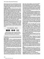
A wave period is one segment from the repeating
sinusoidal cycles
of
the wave taken over time from a
reference point on the wave. The period varies with
the wave - longer wavelengths have longer periods.
In A, the period
of
the wave begins at zero
(0).
In
B,
the wave has been shifted
by
a quarter
of
its
period
such that it
is
referencedfrom the highest
point
in the
wave cycle rather than the
point
at
which it crosses
the X axis.
The length
of
the wave
period
hasn t changed, only
the time point in the phase
at
which it is referenced,
relative to thefirst wave.
If
the two differentphases in
the wavewereplottedon top
of
oneanother, they would
undulate with the same
period
length, shape,
and
am-
plitude - only the phase has been shifted.
By
creating a series
of
shifts in the waves, relative
to the preceding wave, it is possible
to
use each indi-
vidual wave
to
represent a binary value. Thus a half-
period shift
in
a four-phase system changes a 2-bit
binary valuefrom 00 to 10
andfrom
10 to
00.
phase-locked loop
PLL.
A
technology
used
in
sili-
con-based
integrated
circuits
(ICs),
a
PLL
circuit
con-
trols
an
oscillator
at
a
constant
phase
angle
relative
to
a
reference
signal.
The
three
basic
aspects
ofa
digi-
tal
PLL
are
a controllable oscillator, a
filter,
and
a
phase
detector/comparator
combined
within
a
closed-
loop
frequency
feedback
system.
PLLs
are
useful
for
signal
processing
and
synchronization
applications
such
as
controlling
automatic
phase
adjustments
in
a
signal.
The
signal
can
be
referenced
by
the
PLL
in
various
ways;
it
can
be
based
upon
acarrier
signal
or
linear
or
nonlinear
baseband
references.
PLL
was
traditionally
analog,
but
there
are
now
also
digital
versions
and
both
are
suitable
for
various
types
of
applications.
PLL
has
been
around
for
several
de-
cades;
it
is
commonly used
to
synch a reference
broadcast
signal
to
the
horizontal
oscillator ofa
tele-
vision
receiver,
for
example.
Because
it
is
a
basic
tim-
ing
technology,
it
is
found
in
components
ranging
from
voltmeters
and
spectrometers
to
cell
phones
and
space-based
tracking
and
synchronization
systems.
In
communications
devices,
newer
PLL
circuits
sup-
port
products
with
higher
data
transfer
rates,
higher
frequencies,
and
smaller
footprints.
Commercial
dual
phase-locked
loop-based
ICs
are
small,
low-power-
consumption
components
that
can
offer
frequencies
up
to
2.5
GHz
(in
some
cases,
up
to
4.8
GHz),
mak-
ing
them
suitable
for
radio
transceivers
for
a
variety
of
types
ofproducts,
including
cellular
phones
and
pcs.
PLL
ICs
can
also
be
used
as
secondary
circuits
for
providing
intermediate
frequency
radio
waves
that
are
commonly
used
in
cell
phone
receivers.
PLL
circuits
can
be
readily
modeled
in
software
for
educational
and
design
purposes. Java-based
PLL
modelers
are
available
on
the
Web.
Phelps, George M. (1820-1895)
An
American
ma-
chinist
and
inventor
best
known
for
his
telegraphic
key
and
printer
inventions,
although
he
also
designed
stock
tickers
(a
type
of specialized telegraph)
and
early
telephone
equipment.
As
a
youth,
Phelps
was
apprenticed
as
a machinist
to
his
uncle,
Jonas
H.
Phelps,
to
build
scientific
instruments.
The
Phelps
and
Gurley
surveying
instruments
company
evolved
into
Gurley
Precision
Instruments,
which
is
still
in
business.
George
Phelps
set
up
shop
in
1850,
in
Troy,
New
York,
and
began
designing
and
patenting
a
wide
va-
riety
ofprecision
electromechanical
devices,
includ-
ing
telegraph
keys
(e.g.,
a
camelback
key).
He
was
known
for
elegance
of
design
and
superior
workman-
ship.
When
approached
about
improving
upon
the
popular
but
complex
telegraphic
instrument
ofR.E.
House,
Phelps
joined
with
Jarius
Dickerman
to
form
Phelps
and
Dickerman
and
House's Printing
Tele-
graph
Instrument Manufacturer, located
in
Ferry
Street
in
Troy.
Thus,
Phelps
built
House
instruments
for
several
years.
The
American
Telegraph
Company
purchased
the
Phelps
and
Dickerman
holdings,
retaining
Phelps
as
a superintendent. After the American Civil
War,
American Telegraph was purchased
by
Western
Union,
again
retaining
Phelps
for
his
knowledge
and
experience
in
the
field.
Western
Union
also
acquired
735
,xgP
,
l
f
.'
,
'~f
© 2003 by CRC Press LLC
Fiber
Optics
Illustrated
Dictionary
the
patent
rights
to
Phelps' printing telegraph. Phelps
was
assigned
to
work
on
a"harmonic telegraph,"
the
forerunner
to
the
telephone, adevice first patented
in
the
u.s.
by
A.
Graham
Bell.
Phelps
was
an
associate ofThomas Edison
and
cre-
ated
some
of
the
patent models
for
Edison's early
in-
ventions. Phelps became
the
superintendent of
West-
em Union
Telegraph
in
New
York
and
remained
as
a
staff inventor
in
his
later
career.
He
may
also
have
been associated with the Field brothers,
who
were
instrumental
in
laying
the
first successful transatlan-
tic telegraph cable.
See
Phelps Combination Printer.
PHIGS Programmer's Hierarchical Interactive
Graphics
System.
An
official standard
for
3D
graph-
ics
from
the
late
1980s.
The
PHIGS+ extension
added
sophisticated rendering ofrealistic looking objects
on
raster displays. Simple PRIGS (SPRIGS)
is
a
pow-
erful, display-independent subset
of
PRIGS which
in-
corporates
some
PRIGS+ features.
Phillips code A shorthand telegraphic code as-
sembled/revised
from
existing
systems
by
Walter
Polk
Phillips, published
in
1879.
Originally
an
American
Telegraph messenger, Phillips became
an
accom-
plished
press
telegrapher
(2731
wph)
and
his
code
was
widely
used
for
decades.
See
73
in
Numerals
chapter.
phoneme A
unit
of
speech,
considered
to
be
the
small-
est distinguishable unit, which
may
vary
from
lan-
guage
to
language
and
among
dialects
of
aparticular
language. Phonemes
are
of
interest to programmers
for
speech recognition
and
speech generation appli-
cations.
See
speech recognition.
Photo
CD
Kodak Digital Science Photo
CD
System.
An
image storage
and
retrieval format developed
by
Kodak
and
introduced
in
1992.
PhotoCD
is
a means
to
store digitized
still
images
in
various resolutions
on
a compact
disc
so
it
can
be
read back
from
CD-
ROM
drives.
It
is
used
by
many stock photo suppli-
ers
and
graphic design professionals.
Conventional35mm
film
shot
with a traditional cam-
era can be taken to photofinishers supporting
PhotoCD
and
developed
into
both
pictures
and
digi-
tal
images.
At
the
lab,
the
file
is
scanned with a high
resolution drum scanner and saved
onto
Photo
CD
discs.
If
there
is
room, additional pictures can
be
added
to
the
disc
later,
and
read
back
with
a multi-
session CD-ROM
XA
drive
and
an
appropriate soft-
ware driver (including Apple QuickTime Photo
CD
extension,
SOl's
IRIX, Sun's Solaris, IBM's
OS2/WARP,
AmigaOS 3.1,
IBM
AIX,
etc.).
A Photo
CD
disc
can
hold about
100
images, that
is,
about
three
or
four
rolls
of
film.
The
images
are
stored
in
Photo
YCC
color encoding, with multiple resolu-
tion
levels. Pixel resolutions include:
2048
x 3072,
1024
x 1536,512 x
768,
256
x
384,
128
x
192.
The
Photo
CD
Pro
format also includes
4096
x
6144.
See
compact
disc.
Photocopy Machine - Original Invention
C.
F.
CARLSON
~L£CfllOrIiOTOORArIlT
Pll
April
-I. lt311
Oct. 6, 1942.
INVENTOR
2,297,691
OeL
6,
1942.
C,
P.
C""LSOH
1;l.CCfllOfltOTOGurtty
'Ilel!
AprIl
'i.
II;»
2,297.691
The 1942 Carlson patentshows the various basic parts
of
a photocopier (right), with a detail
of
the drum mecha-
nism (left). Large companies were not willing
to purchase the new technology. A small company calledXerox did!
736
© 2003 by CRC Press LLC
photocopyA
dry
transfer
replication
process
from
an
optically
imaged
source, sometimes
also
called a
xerograph,
after
Xerox,
the
company
that
popularized
the
technology.
C.F.
Carlson
was
awarded
a
patent
for
a
photocopy
invention
in
1942
and
failed
to
sell
it
to
some
of
the
larger
business-oriented
companies.
But
a
small
company
called
Xerox
took
a
chance
on
the
technology.
See
the
Carlson
patent
diagram.
photodetector
PD.
A
component
or
biological
sys-
tem
that
responds
to
stimulation
by
light.
Plants
have
photosensitive
structures
and
mechanisms
that
enable
them
to
detect
sunlight
and
orient
themselves
towards
it
and
certain
natural
and
synthetic materials
have
photodetecting
properties
that
can
be
incorporated
into
industrial
device
assemblies.
Since
light
has
a
number
of
wave-like
and
particle-like
properties
and
emits
heat
at
different
levels
depending
upon
loca-
tion
and
time
of
day,
the
definition
ofphotodetector
is
somewhat
broad,
reflecting
the
capability
of
react-
ing
to
the
presence
oflight
without
necessarily
speci-
fying
what
aspect
of
light
is
causing
the
reaction.
In
general,
photodetectors
are
subclassified
as
thermal
detectors
and
photon
detectors.
Simple
photodetector
components
may
respond
only
to
the
presence
(or
absence)
of
light
within
certain
pa-
rameters
and
some
may
be
sensitive
to
light
without
discriminating
its
intensity
or
character.
More
sophis-
ticated
photo
detectors
may
be
"tuned"
to
detect
spe-
cific
wavelengths
or
regions
of
wavelengths
and
some
are
also
sensitive
to
the
magnitude
ofa
light
stimu-
lus.
Even
at
its
most
basic
level,
however,
photode-
tection
is
an
important
capability
at
the
heart
of
many
systems.
Photodetectors
are
widely
used
in
imaging
devices,
security
systems,
robotic
vision,
and
signal-
ing
and
transmission
systems.
In
practical applications, the response
of
a
photodetecting
substance
is
often
very
weak
and
may
require
further
processing
to
make
it
useful.
Ampli-
fication
of
very
subtle
reactions
to
light
has
limits,
due
to
noise
that
is
introduced
when
a
weak
signal
is
amplified.
Much
of
semiconductor
technology
is
de-
voted
to
improving
the
signal-to-noise
ratio
of
am-
plified
signals.
In
addition,
photodetectors
are
often
environmentally
sensitive.
Light
is
ubiquitous
and
it
is
often
challenging
to
detect
only
that
light
that
is
of
interest.
For
example,
athermal-sensitive
detector
in
a
hot
environment
such
as
a
desert,
may
need
to
be
cooled
in
order
to
detect
other
sources
of
light
(e.g.,
a
signal
light).
An
astronomical
photo
detector
(for
studying
light
from
celestial
bodies)
works
more
ef-
fectively
if
placed
in
orbit
around
the
Earth
rather
than
in
the
observatory
ofa university
in
the
middle
ofa
large
city,
due
to
the
interaction
of
ambient light
sources.
Depending
upon
the
type
of
detector, commercial
photo
detectors
are
typically
described
in
terms
of
re-
sponsivity
(the
sensitivity
and
magnitude
oftheir
re-
action
to
light),
efficiency
(how
much
signal
is
gen-
erated
per
photon
stimulus),
response
time,
signal-to-
noise
ratios
and
types
of
noise
(e.g.,
Johnson
noise),
and
the
linearity
of
the
response.
Figures
of
merit
may
also
be
used.
Film
photography
is
an
example
of
directly
harness-
ing
the
selective
photosensitivity
of
certain
chemicals
by
embedding
them
in
a
film
substrate
and
briefly
exposing
them
to
light.
The
image
captured
in
film
can
then
be
transferred
to
paper
by
yet
another
pho-
tosensitive process
(with
stray light
excluded
in
a
darkroom).
Sometimes
photodetection
is
only
one
step
in
a
series
of
detection
and
conversion
processes.
F
or
example,
a
scintillating
device
that
converts
elec-
tromagnetic
energy
outside
the
optical
spectrum,
such
as
X-rays,
into
optical wavelengths,
may
feed
the
signal
to
a
photodetector.
From
there
it
may
go
to
a
photomultiplier that further converts
the
signal
to
electrical
impulses.
Thus,
a photodetector
assembly
can
indirectly
detect
wavelengths
outside
the
optical
spectrum.
A
complex
light
impulse
can
be
characterized
by
us-
ing
a
device
in
which
multiple photo
detectors
are
tuned
to
respond
to
different
optical
frequencies.
The
data
derived
from
individual
elements
in
the
photo-
detector
array
can
be
signal
processed
to
produce
a
complex
overall
statistical picture of
the
light-emit-
ting
characteristics of
sample
specimens
or
light-car-
rying
transmissions
media.
The
creation
of
semiconductor
photo
detectors
is
as
much
art
as
science
and
much
of
the
fabrication
is
at
the
molecular
level,
crossing
boundaries
in
geology,
quantum
physics,
chemistry,
and
biology.
Structures
for
photo
detectors
can
be
grown
in
molecular
beam
epitaxy
(MBE)
systems
on
semi-dielectric
substrates.
Such
components
are
being
developed
for
new
high-
speed
photodetectors, giving
them
properties
for
meeting
the
greater
bandwidth
and
distance
demands
of
microwave
fiber
optic
links.
See
photoelectric
cell,
phototube,
thermopile,
traveling-wave
tube.
photodiodeA
semiconductor
photodetector
compo-
nent
for
converting
light
energy
into
electrical
energy.
See
photodetector.
Sample
Photodiodes
/ /
/
Photodiodes
are
semiconductorphotodetecting
com-
ponents. They come
in
a wide variety
of
shapes,
sizes,
andlevels
of
sensitivity
to
photonic
energy.
Illustrated
here
are
common
configurationsfor a
gallium-arsenide
diode
(left)
and
an
indium-gallium-arsenide
diode.
photodiode, avalanche
APD.
A
semiconductor
com-
ponent
commonly
made
of
silicon
(Si)
or
indium-
737
© 2003 by CRC Press LLC
Fiber
Optics
Illustrated
Dictionary
gallium-arsenide/indium-phosphide
(InGaAs/InP).
Silicon
APDs
are
p-n
junction
solid-state
detectors
with
high
internal
gain.
They
are
reasonably
immune
to
electric
fields
and
sensitive
enough
to
detect
single
photons
at
room
temperature.
APDs
are
used
for
optical
detection
for
a
variety
of
applications
including
fiber
optic
communication
re-
ceivers, fluorescence detectors, photon counters,
time-of-flight
ranging
devices,
and
cryptography.
Fi-
ber
optic
receivers
commonly
use
p-i-n
photodiodes
or
APDs
for
detecting
and
converting
an
optical
sig-
nal
into
an
electrical
signal.
New
indium-gallium-arsenide/silicon
(InGaAs/Si)
APDs
have
been
developed
under
a
grant
funded
by
AFRL/DARPA
with
separate
absorption
and
multi-
plication
(SAM)
regions
for
use
in
near-infrared
fre-
quencies.
These
offer
faster,
more
sensitive
photode-
tection
at
wavelengths
that
were
not
previously
prac-
tical.
See
avalanche
diode,
Zener
diode.
photoelectric
cell
A
type
of
electronic
sensing
device
activated
by
light
and
widely
used
in
security
systems,
automatic
lighting
systems
(e.g.,
street
lights),
auto-
matic
doors,
etc.
A
photoelectric
cell
can
be
made
by
coating
cesium
on
one
of
the
electrodes
in
a
vacuum
tube.
This
technology
was
used
in
early
television
cameras.
See
photo
detector.
photography
The
art
and
science
of
registering
light
from
objects
in
a
scene
and
storing
them
in
the
form
of
an
image.
Later
it
became
possible
to
produce
multiples
of
these
images
by
a
number
of
means.
Most
photography
involves
capturing
three-dimensional
imagery
in
a
two-dimensional
format.
Light
is
usu-
ally
recorded
from
the
visible
spectrum,
but
there
are
cameras
and
films
designed
to
record
heat
and
infra-
red
radiation
which
show
images
in
a
form
different
from
the
way
humans
perceive
them,
and
electron
microscopes record
the
movement of a beam of
electrons.
Traditional
photography
was
developed
in
the
early
1800s
by
a
number
of inventors including
Joseph
Nicephone
Niepce,
a
French
inventor,
who
developed
a
process
called
heliography
or
sun
drawing,
on
pa-
per
coated
with
silver
chloride.
Other
pioneers
in-
cluded
Daguerre
(originator of
the
daguerreotype),
Herschel,
Talbot,
and
Archer.
One
of
the
earliest
pho-
tos
was
captured
with
silver chloride
by
Thomas
Wedgewood
in
1802.
More
than
150
years
passed
be-
fore
3D
photography,
in
the
form
of
holographs,
be-
came
practical.
Newer
digital
cameras
can
immedi-
ately
relay
an
image
to
a
computer
network
so
the
image
can
be
viewed
almost
instantly
at
great
dis-
tances
from
the
actual scene of the event.
See
Daguerre,
Louis
Jacques
Mande;
heliography.
photometerAn
instrument
for
determining
the
inten-
sity
of
transmitted
or
reflected
light,
sometimes
called
an
opticalpower
meter.
A
photometer
is
a
type
of
ra-
diometer
and
photometers
that
measure
the
intensity
of
frequencies
beyond
the
human
visual
range
are
sometimes
termed
radiometer/photometer
devices.
Photometers
are
used
in
scientific
research,
photog-
raphy,
and
many
aspects
of
experimental
and
com-
mercial
optics.
Human
visual
senses
are
quite
good
738
at
determining
relative
brightness,
but
photometric
instruments
are
needed
to
make
objective
assessments
of
light
intensity
within
and
beyond
the
human
vi-
sual
range.
Photometers
come
in
many
shapes
and
sizes
from
simple
photography
or
classroom
models
to
high-end
scientific
research
instruments.
They
may
be
used
to
measure
power
levels
in
laser
beams,
optical
signals
in
modulated
light
beams,
and
solar
radiation.
Pho-
tometers
are
used
to
measure
the
intensity of
traffic
lights
(which
may
dim
over
time)
to
make
sure
they
are
bright
enough
to
be
seen
clearly
by
motorists.
Goniophotometers
are
common
in
the
lighting
indus-
try.
Photometers
aid
in
assessing
light
propagation
through
different
types
of
waveguides
in
the
design
and
development
of
optical
network
technologies.
The
range
of
sensitivity
ofa
photometer
is
dependent
upon
its
price
and
intended
application.
The
spectral
range
within
which
it
is
sensitive
also
varies,
but
com-
monly
photometers
measure
visible
and
infrared
fre-
quencies.
A
basic
classroom
photometer
may
include
several
measurement
scales
with
sensitivity
to
power
levels
ranging
from
about
20
microwatts
to
20
milli-
watts.
Measurement
scales
may
be
linear
or
logarith-
mic.
Some
industrial
photometers
have
optional,
in-
terchangeable
sensor
heads
for
different
applications.
Simultaneous
measurements
of
more
than
one
wave-
length
are
possible
with
some
scientific
models.
The
reading
from
a
photometer
may
be
output
to
a
built-
in
LCD
display
or
may
be
transmitted
to
other
devices
such
as
oscilloscopes,
recorders,
or
computer
periph-
eral
cards.
Photometers
designed
for
microscopes
may
have
an
adjustable
iris
to
enable
the
sample
to
be
viewed
while
the
light
is
measured.
A
housing
for
filters
may
also
be
included.
In
astronomy,
where
light
intensity
provides
informa-
tion
on
the
properties
of
celestial
bodies,
photometers
are
important
research
tools
and
may
be
integrated
with
spectrographs
in
telescopic
systems.
Sophisti-
cated
optical
fiber-based
photometers
are
now
avail-
able
for
studying
fast
variable
astronomical
phenom-
ena.
Multiple
fibers
enable
reference
images
to
be
as-
sessed
in
conjunction
with
the
phenomena
being
ob-
served.
Fiber
optics
may
be
used
to
link
individual
telescopes
in
a
telescopic
array.
The
first known drawing of a photometer
was
by
Peter
Paul
Rubens,
who
illustrated a
book
on
optics
by
F.
d'
Aguilon,
published
in
1613.
P.
Bouguer
de-
scribed
several
simple
photometers
in
a
treatise
pub-
lished
posthumously
in
1760.
This
was
an
expansion
of
an
earlier
essay,
published
in
1729
and
Bouguer
is
considered
by
many
to
be
the
inventor
of
the
photom-
eter.
1 0.
Colladon
developed
a
practical
application
of a
photometer
for
his
engineering
proj
ects
in
the
mid-1800s.
Prism-based
spectrophotometers
became
available
on
the
market
after
World
War
II
but
the
technology
remained
relatively
limited
and
expensive
until
the
1960s,
when
grating spectrophotometers
became
available.
Since
then
advancements
in
elec-
tronics
have
made
photometers
increasingly
small
and
powerful.
By
the
1990s,
built-in
filters,
exchangeable
© 2003 by CRC Press LLC
sensing
heads,
LCD
displays,
and
computer
interfaces
were
readily
available.
Fiber
optics
and
lasers
are
now
incorporated
into
a
number
of
types
of photometers. For
example,
in
chemical
photometry,
a laser
can
be
used
as
a
light
source
for
illuminating
a
sample
to
measure
its
pho-
tometric
characteristics.
When
the
coherent
light
hits
the
obstacle
(sample),
the
light
is
scattered
and
may
be
detected
by
a
fine
fiber
filament
that
directs
the
light
that
enters
the
fiber
to
a
photomultiplier,
where
it
is
passed
on
to
a
processing
system
and
display.
See
Aguilon,
Fran~ois
de;
Bouguer,
Pierre;
luminance;
photopolarimeter;
radiometer.
photomultiplier
PM.
A light-sensitive
component
that
emits
electrons
in
response
to
stimulus
by
pho-
tons
(of
sufficient
energy
levels).
This
is
a
very
use-
ful
means
to
convert
electromagnetic
energy
in
the
optical
spectrum
into
electrical
energy
that
can
be
used
to
activate
and
control
other
components.
photomultiplier tube
PMT.
Typically,
an
evacuated
glass
component
containing
a
photocathode
that
emits
electrons
when
subjected
to
photonic
energy
suffi-
cient
to
trigger
aphotoelectric
effect.
The
photocath-
ode
operates
at
a
high
negative
voltage
and
the
elec-
trons
emitted
are
accelerated
towards
a
series
(chain)
of
dynodes
that
are
positioned
along
the
electron
path
between
the
electron-emitting
cathode
and
the
elec-
tron-attracting
anode.
The
dynodes
generate
addi-
tional
electrons
through
secondary-emission
multipli-
cation.
PMTs
can
be
configured
with
multiple
anodes,
ar-
ranged
in
linear
(e.g.,
1x
16)
or
grid
patterns
(e.g.,
8x
8)
for
use
with
fiber
faceplate
scintillating
appli-
cations,
for
example.
Photomultiplier
tubes
can
respond
to
a
wide
range
of
wavelengths
from
ultraviolet
to
infrared,
but
respon-
sivity
and
emission
effectiveness
are
dependent,
in
part,
upon
the
materials
used.
In
general,
PMTs
are
fast-response,
low-noise
components
practical
for
a
wide
variety
of
applications,
including
laser
technol-
ogy,
radiation
measurement,
spectroscopy,
high
en-
ergy
physics
research,
and
others.
Photomultipliers
are
sensitive
enough
to
count
pho-
tons
at
very
low
light
levels
(down
to
one
photon)
and
thus
are
highly
efficient
at
distinquishing
signal
from
noise.
Thermal
noise
can
be
reduced
by
cooling
and
ambient
light
and
magnetic
interference
can
be
re-
duced
with
proper
shielding.
Commercial
photomultiplier
tubes
commonly
have
14,
20,
or
21
pins.
The
primary
connections
are
to
the
10,12,
or
14
dynodes,
the
anode,
cathode,
focus
elec-
trode,
and
shield.
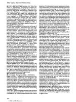
Simplified Drawing ofBasic Photomultiplier
Components
and
Dynode
Function
photocathode
anode
photocathode
anode
This is a highly simplifieddraWing
of
a basicphotomultiplier tube usedto convert
and
amplify aphotonicsignal.
The photocathode
at
the top converts electromagnetic energy in theform
of
photons into electron emissions which
are attractedto the anode
at
the base
of
the tube.
As
the electrons travel towardthe anode, they encounter a series
of
dynodes in the middle 0/the tube, poweredwith voltages that are calibratedto one anotherto control the magnitude
o/electron emissions.
As
an electron/rom the cathode (or the precedingdynode) hits a dynode, it is reflected along
with secondary emissions governed by the voltage applied
to
the dynode to the next dynode in the chain, causing a
cumulative amplification
of
the signal. When the electrons reach the anode, the signalisprocessed
by
a smallcircuit
within the base
and
output through the contacts comingfrom the bottom
of
the base to inteiface with other compo-
nents (21-pin sockets are common). A magnetic shield thatfits over the base can shield the electrical circuitsfrom
external inteiference.
As
illustratedin the line diagrams, the voltages appliedto the reflective dynodes are relatedto
the number
of
electrons emitted, with higher voltages (right) providing greater gain (within operating limits).
Thus, very weaksignals, even as smallas onephoton, can
be
measured
and
manipulatedwithphotomultipliers to
facilitate research in particle physics
and
to fabricate sensors,
and
scientific
and
industrial quality assurance,
testing,
and
sampling instruments.
739
© 2003 by CRC Press LLC
Fiber
Optics
Illustrated
Dictionary
A
phototube
is
a
simpler
version
of
the
photomulti-
plier
tube
(without
dynodes).
See
dynode,
photo-
sensor.
photomultiplier tube base A
mechanical
and
volt-
age
distribution/dividing
component
for
coupling
with
a
photomultiplier
tube.
The
tube
base
may
op-
tionally
include
a
magnetic
shield
to
protect
it
from
Earth-
and
equipment-originating
magnetic
fields.
The
shield
may
also
protect
the
coupled
photomulti-
plier
tube
from
ambient
light
and
magnetic
emissions.
The
photomultiplier
tube
typically
connects
to
the
base
through
14
or
21
pins.
Outputs
from
the
base,
such
as
connections
to
the
anode
or
a
specific
dyn-
ode,
are
typically
through
50-ohm
coaxial
connec-
tions.
Some
versions
include
low-noise
preamplifi-
ers
incorporated
into
the
base
for
use
with
scintilla-
tion
detectors.
Photomultiplier
tube
bases
have
also
been
designed
for
use
with
multiple
photomultiplier
tubes
(e.g,
in
arrays).
Voltages
for
the
tubes
in
the
assembly
may
PhotoPhone
-
Bell
and
Tainter's
Light-Based
Communications Invention
A.
G,
BELL"
S.
TAINTER.
Photophone
Transmitter.
Patented
Dec.
14.
1880.
:J:i?~.t.
No.
235,.496
•
:, _ ~
,
~
_.
~ I
Jl
J
The
Photophone
was
based
upon
the concept
of
using light
as
amediumforthe transmission
of
sound.
Sunlight was
used
to
translate acoustic vibrations into light signals
that
were
reflected
to
a receiver where they
were
converted
to
electrical signals
through
the use oflight-sensitive selenium
(the
same material usedfor early television inventions).
By
substituting aparabolic surface, Bellfound
he
could
increase
the
intensity
of
the
signals and
was
able
to
transmit
signals over adistance
of
several hundredmeters
on
asunny
day.
Bell
was
very excitedabout thepotential
of
wireless
communications and took out four patents
on
the
Photophone with assistance
from
Sumner
Tainter.
{Library
of
Congress
American Memory Collection and
U.S.
Patent Office (upper right).]
740
© 2003 by CRC Press LLC
be
controlled individually,
in
groups,
or
unison.
Cockcroft-
Walton
voltage
multipliers
have
been
sug-
gested
in
place
of
resistive
voltage
dividers
for
PMTs
that
are
densely
packed,
in
order
to
minimize
dissi-
pated
power.
See
dynode,
photomultiplier
tube.
photombltiplier
tube
chamber
A
housing
for
physi-
cally
protecting,
electromagnetically
shielding,
and
cooling
photomultiplier
tubes.
Depending
upon
the
temperatures required, the housing
may
include
single-
or
double-paned
windows
to
prevent
conden-
sation
or
icing.
A
variety
of
materials
are
available
for
the
windows,
including
Plexiglas®,
Pyrex™,
or
fused
silica.
Fused
silica
is
effective
over
a
broader
spectrum
of
wavelengths.
See
photomultiplier
tube.
photonic crystal A photonic
bandgap
technology
described
and
developed originally
by
E.
Yablo-
novitch,
developed
further
by
Ozbay
at
Ames
Labo-
ratory,
Southampton
Researchers,
S.
Kawakami
and
his
collaborators
in
Japan,
and
a
number
of
others.
These
photonic
crystals
have
periodic
dielectric
struc-
tures
that
exhibit
large
anisotropy,
high
dispersion,
and
photonic
bandgap
properties.
The
bandgap,
which
is
similar
in
concept
to
gaps
in
semiconductor
devices
with
a lattice-like structure
and
holes
or
"wells,"
makes
it
possible
to
selectively
filter
certain
optical
frequency
ranges
by
means
not
available
with
con-
ventionallenses
or
existing
semiconductors.
Varying
the
refractive
index
of
the
component
or
in-
troducing
point
defects
within
an
othelWise
perfect
dielectric
structure
have
the
potential
for
localizing
light,
essentially
trapping
it
selectively.
The
size
of
the
holes
could
further
be
controlled
to
manipulate
energy
levels.
Yablonovitch
et
al.
have
further
de-
scribed
how
3D
circuit
designs
could
extend
the
tech-
nology
into
lower
wavelengths.
In
2002,
Chen
and
Suzuki
described
an
integrated
fiber-photonic
crys-
tal
system
with
a
uniform
bandgap
and
low
insertion
loss.
This
has
potential
for
optical
switches
and
rout-
ers.
Also
in
2002,
OFS
Laboratories
introduced
a
new
fiber
design
incorporating a photonic
bandgap
for
tuning
the
transmission
through
the
fiber.
There
is
much
excitement
surrounding
photonic
crys-
tal
technology.
It
has
been
suggested
that
highly-ef-
ficient
light
reflectors
for
fiber
optics
transmission
sources
(e.g.,
LEOs)
and
computers
operating
in
the
hundreds
of
terahertz
computing
range
could
be
de-
signed
with
the
technology.
MIT
has
developed
freely
available
software
to
model
the
dispersion
relations
in
photonic
crystals
in
order
to
visualize
the
band
structures.
It
is
available
for
download online
as
MIT
PHotonic-Bands. See
Kawakami,
Sujiro;
photonic
crystal
fiber.
photonic
crystal
fiber
PCF.
A type
of
micro-
structured optical fiber with low-index refractive
materials
fabricated
within higher-index materials
(e.g.,
silica).
They
may
be
categorized
as
low
index
(photonic
bandgap)
or
high
index
guiding
fibers
that
produce
total
internal
reflection
through
a
lower
ef-
fective
index.
PCFs
were
first
demonstrated
in
the
mid-l
990s
and
have
made
it
easier
to
harness
the
properties
inherent
in
optical
transmissions
through
novel
fiber
fabrica-
tion patterns. Dispersion properties, linearity, a
broader
range
of
numerical
apertures,
and
other
fac-
tors
can
be
utilized
and
better controlled
through
PCFs,
increasing
the
practical
range
of
optical
com-
ponents
and
telecommunications
devices
that
can
be
devised.
See
photonic
crystal.
Photonic
Information
Processing Systems
Labo-
ratory
PIPS.
A
research
lab
founded
by
N.A.
Riza,
a
pioneering
optical
engineer,
at
the
School
of
Optics
and
Center
for
Research
and
Education
in
Optics
and
Lasers
(CREOL)
at
the
University
of
Central
Florida.
The
School
of
Optics
offers
interdisciplinary
gradu-
ate
programs
in
optics.
See
Riza,
Nabeel.
/>Photonics
Components
and
Subsystems
Newsletter
PCSN.
Global
coverage
of
technology,
applications
and
photonics
markets.
Published
monthly
by
Infor-
mation
Gatekeepers,
Inc.
PhotophoneA
historic
device
that
transmitted
voice
by
means
of
light
waves,
invented
by
A.
Graham
Bell
in
1880.
Charles
Sumner
Tainter,
an
experienced
sci-
entific
instrument-maker,
had
a
significant
hand
in
the
practical
embodiment
of
the
idea.
Bell
put
great
stock
in
the
invention,
filing
for
four
patents
for
the
device
and
its
associated
selenium
cells.
The
concepts
are
still
sound
and
the
invention
ahead
of
its
time
and
worth
mentioning
in
detail.
At
least
as
early
as
1878,
Bell
was
developing
the
idea
for
the
Photophone.
He
described
the
possibility
of
"hearing
a
shadow"
by
the
action
of
interrupting
a
~:e~
~:::~~~~~:it°~:~~~~u~
i~:e~C:~1:~ir~
•
May
1878.
In
January
1879,
he
wrote
a
note
describ-
ing
how
he
had
worked
out
the
idea
as
"
the
art of
causing
electrical
signals
and
audible
sounds
in
distant
places
by
the
action
of
light.
It
has
been
discovered
that
certain
substances
such
as
silenium
[sic]
have
their
electrical
resistance
af-
fected
by
light.
When
a
peice
[sic]
of
silenium
in
a
crystalline
con-
dition
is
placed
upon
the
circuit
with
a
telephone
and
voltaic
battery
a
sound
is
audible
from
the
tele-
phone
when
a
beam
of
light
is
allowed
to
fall
upon
the
silenium.
When
a
galvonometer
is
substituted
for
the
tele-
phone
the
needle
is
deflected indicating
the
in-
crease
of current,
when
the
light
falls
upon
the
silenium
thus
showing
that
the
electrical
resistance
of
the
silenium
is
diminished
under
the
action
of
light.
My
invention
consists
in
utilizing
this
property
of
silenium
for
the
purpose
of
causing
telegraphic
sig-
nals
from
a
galvenometer
[sic]
or
audible
sounds
from
a
telephone
in
distant
places
without
the
ne-
cessity
ofa
conducting
wire
between
the
transmit-
ting
and
receiving
stations
The
transmitting
instrument
consists
ofa
power-
ful
~
source
of
light
and
of
an
apparatus
for
interrupting
or
varying
its
intensity.
The
receiving instrument consists of a
lens
by
means
of
which
the
distant
light
is
focussed
[sic]
upon
a peice
of
crystalline silenium,
which
is
741
© 2003 by CRC Press LLC