Model-Based Design for Embedded Systems- P23 doc
Bạn đang xem bản rút gọn của tài liệu. Xem và tải ngay bản đầy đủ của tài liệu tại đây (768.39 KB, 30 trang )
Nicolescu/Model-Based Design for Embedded Systems 67842_C019 Finals Page 636 2009-10-14
636 Model-Based Design for Embedded Systems
2.5 5 7.5 10 12.5 15 17.5 20
BPT 32 S
1
– 1.1μm pitch
BPT 45 S
1
– 1.1μm pitch
BPT 65 S
1
– 1.1μm pitch
BPT 32 S
2
– 1.1μm pitch
BPT 45 S
2
– 1.1μm pitch
BPT 65 S
2
– 1.1μm pitch
Static power (mW) vs. interconnect length—optical link
Link length (mm)(a)
(b)
30
25
20
15
10
5
0
1.4E – 02
1.2E – 02
1.0E – 02
8.0E – 03
6.0E – 03
4.0E – 03
2.0E – 03
0.0E + 00
2.5 5 7.5 10 12.5 15 17.5 20
BPT 32 S
1
– 1.1μm pitch
BPT 45 S
1
– 1.1μm pitch
BPT 65 S
1
– 1.1μm pitch
BPT 32 S
2
– 1.1μm pitch
BPT 45 S
2
– 1.1μm pitch
BPT 65 S
2
– 1.1μm pitch
Dynamic power (W) vs. interconnect length—optical link
Link length (mm)
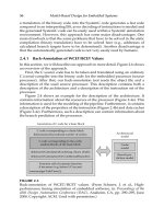
FIGURE 19.13
Power vs. interconnect length for BPT 65, 45, and 32 nm technologies
(a) Average static power (in mW). (b) Average dynamic power (in W).
and to lower detector capacitance, which lowers the receiver circuit quiescent
current.
Dynamic power reductions between S
1
and S
2
, of the order of 2–4, are
observed. This is attributed mainly to lower transistor capacitances because
of lower bias current in the driver (due to the reduction in source threshold
current) and because of lower modulation currents in the driver (due to the
increase in source efficiency and detector responsivity).
Nicolescu/Model-Based Design for Embedded Systems 67842_C019 Finals Page 637 2009-10-14
Platform for Model-Based Design of Integrated Multi-Technology Systems 637
45
40
35
30
25
20
15
10
5
0
2.5 5 7.5 10
Link length (mm)(a)
(b)
Total power (mW) vs. interconnect length—optical link
12.5 15 17.5 20
BPT 32 S
1
–1.1μm pitch
BPT 45 S
1
–1.1μm pitch
BPT 65 S
1
–1.1μm pitch
BPT 32 S
2
–1.1μm pitch
BPT 45 S
2
–1.1μm pitch
BPT 65 S
2
–1.1μm pitch
BPT 65
S
1
–1.1μm pitch
BPT 45
S
1
–1.1μm pitch
BPT 32
S
1
–1.1μm pitch
BPT 65
S
2
–1.1μm pitch
BPT 45
S
2
–1.1μm pitch
BPT 32
S
2
–1.1μm pitch
10
9
8
7
6
5
4
3
2
1
0
Link length (mm)
Power reduction factor vs interconnect length
0 5 10 15 20 25
FIGURE 19.14
(a) Total power (in mW) vs. interconnect length for BPT 65, 45, and 32 nm
technologies. (b) Average total power comparison for varying interconnect
length and technologies at 1.1 μm pitch: reduction factor.
Using static and dynamic power information, the total energy can be cal-
culated (Figure 19.14).
The overall power is shown to be reduced between S
1
and S
2
by fac-
tors of between 2 and 4. The greatest reduction is achieved at higher link
lengths, which is the expected context for the use of such optical links. For
Nicolescu/Model-Based Design for Embedded Systems 67842_C019 Finals Page 638 2009-10-14
638 Model-Based Design for Embedded Systems
S
2
, power reduction can be considered to be a major argument in favor of
optical interconnect. For S
1
, it is clear that the static power comparison is
the weak point for optical interconnect, because of continuous biasing of the
source (avoiding turn-on times to achieve the required bit rate) and of the
receiver circuit (the circuit bandwidth is directly related to quiescent bias
current). The reduction in source threshold current and in detector capaci-
tance in S
2
has a significant impact on both these factors, to the extent that the
static power in optical links, while still higher than that of electrical intercon-
nect, is no longer dominant. Dynamic power in optical interconnect is further
reduced with the smaller overall circuit transistors used in this analysis. The
total power comparison shows power reduction factors between 5x and 10x
for link lengths above 10 mm and for the two most advanced technology
nodes. It is likely that comparisons using technologies with transistor gate
lengths below 32 nm will further improve this comparison since on the elec-
trical side the static power dissipation will increase with leakage current. We
can thus consider that the optical device improvements constitute the main
path to the solution to the following recommendation: “Power, and partic-
ularly static power, is a key performance metric to optimize during explo-
ration of optical interconnect device specifications.” This is an illustration of
the type of feedback our approach can give to photonic device engineers.
19.5 Conclusions and Ideas for the Future
In this chapter, we have looked at several aspects of heterogeneous design
methods in the context of increasing diversification of integration technolo-
gies. The rationale and analysis of the situation in terms of technological evo-
lution and severe gaps in design technology show a clear need for advances
in this domain. The experimental Rune
II
heterogeneous design platform
addresses some of these needs—in particular we have shown how design
processes can be formalized over multiple abstraction levels and multiple
domains using a common model for design knowledge formulation called
AMS/MT IP. To address the need to represent this knowledge at higher
abstraction levels in order to retain compatibility with system-level design
methods, we have demonstrated the feasibility of the use of UML and estab-
lished parallels between the UML concepts and widely used concepts in
AMS/MT descriptions. We have successfully used these concepts to build
class diagrams for functional and structural models of integrated optical
link component libraries, and implemented a synthesis scenario to explore,
in a quite detailed way, the available design space over a number of very
different dimension types. This design method and technology is partic-
ularly useful for the repetitive design of fixed optical link structures sub-
ject to varying design constraints, technology parameters, and performance
Nicolescu/Model-Based Design for Embedded Systems 67842_C019 Finals Page 639 2009-10-14
Platform for Model-Based Design of Integrated Multi-Technology Systems 639
requirements. We have illustrated the direct application of our approach for
optical link synthesis and technology performance characterization by ana-
lyzing optical link performance for two sets of photonic component parame-
ters and three CMOS technology generations. Importantly for technological
development, the results of such analyses can generate useful feedback from
system designers to component designers.
In our view, the next major step in technological evolution for SoC con-
cerns 3D integration. This approach, exploiting the vertical dimension, pro-
vides an opportunity to continue to achieve the performance levels predicted
by the extrapolation of Moore’s law, but using a different technological
approach. The main impact is to enable the construction of highly complex
systems (e.g., multiple core data-processing systems with multiple memory
banks in close spatial proximity; highly heterogeneous systems using mul-
tiple technologies for specific functional layers) while reducing the cost of
communication by several orders of magnitude. The direct consequences of
this approach are to (1) improve isochronous signal coverage and (2) allow
evolution toward modular integrated systems. Such an approach should also
in the long term enable novel vertical interconnect solutions (e.g., embedded
repeaters, vertical switches, etc.). While by no means technologically simple,
it does represent a major design paradigm shift away from the conventional
approach of traditional Moore’s law scaling toward “equivalent scaling” and
“functional diversity” through unconventional approaches.
In this context, several tradeoff situations can be clearly shown to require
heterogeneous design methods, which cannot as yet be processed by existing
tools. Some examples are given here.
• Tradeoffs for data-processing systems using, for example, 45 nm
CMOS for processor cores and a specific technology (Flash–DRAM) for
memory. While the gain over conventional planar architectures is clear
(high core-memory bandwidth and high memory capacity leading to
reduction/elimination of cache structure, enabling orders of magni-
tude improvements in processing time for algorithms requiring high
data-rate memory access), the organization of the memory and its spa-
tial organization in relation to achievable through-silicon via (TSV)
density and characteristics, and to the number and size of processor
cores, has to be explored.
• Partitioning in transformations from a planar chip to a 3D architecture.
It will, for example, be necessary to explore comparisons between a
complete system on chip built from an aggressive planar CMOS tech-
nology and a technological partition between using the same aggres-
sive CMOS technology for data processing, but a less aggressive, more
stable CMOS technology for I/O functions, analog, power, voltage reg-
ulators to achieve interfacing and to compensate for variability, etc.
The tradeoffs here concern cost, variability, performance, power, and
process simplification.
Nicolescu/Model-Based Design for Embedded Systems 67842_C019 Finals Page 640 2009-10-14
640 Model-Based Design for Embedded Systems
• Tradeoffs for mobile computing nodes in a 3D context using, for
example, an aggressive CMOS technology for processor cores, specific
advanced technology for memory, mature technology for analog, and
a specific technology for RF (e.g., passive RF MEMS). Here, the focus is
on overall power minimization exploiting the reduced communication
cost between the data-processing layer(s) (interpreting received
symbols with more complex interpolation functions) and the RF layer
(relaxed constraints on RF MEMS tunability and speed based on algo-
rithm efficiency).
Acknowledgment
This work was partially funded by the European FP6 IST program under
PICMOS FP6-2002-IST-1-002131.
References
[BIN2005] P. R. A. Binetti et al., A compact detector for use in photonic
interconnections on CMOS ICs, in Proceedings of the Symposium
IEEE/LEOS (Benelux Chapter), Mons, Belgium, 233–236, 2005.
[CAR2004] C. T. Carr, T. M. McGinnity, and L. J. McDaid, Integration of
UML and VHDL-AMS for analogue system modeling, BCS For-
mal Aspects of Computing, 16(1), 80–94, 2004.
[CHA2004] V. Chaudhary, M. Francis, W. Zheng, A. Mantooth, and L.
Lemaitre, Automatic generation of compact semiconductor
device models using Paragon and ADMS, in Proceedings of the
IEEE International Behavioral Modeling and Simulation Conference
(BMAS) 2004, San Jose, CA, 107, 2004, IEEE, Piscataway, NJ.
[ENI2007] Strategic Research Agenda, European Nanoelectronics Initia-
tive Advisory Council (ENIAC), 2007.
[FU2004] T. Fukazawa et al., Low loss intersection of Si photonic wire
waveguides, Japanese Journal of Applied Physics, 43(3), 646–647,
2004.
[FUJ2000] R. Fujita, R. Ushigome, and T. Baba, Continuous wave lasing in
GaInAsP microdisk injection laser with threshold current of 40
μA, Electronics Letters, 36(9), 790–790, 2000.
Nicolescu/Model-Based Design for Embedded Systems 67842_C019 Finals Page 641 2009-10-14
Platform for Model-Based Design of Integrated Multi-Technology Systems 641
[GIE2005] G. Gielen et al., Analog and digital circuit design in 65 nm
CMOS: End of the road? in Proceedings of the Design Automation
and Test in Europe, Munich, Germany, 2005.
[GIR2002] G. Girault and R. Valk, Petri Nets for Systems Engineering,
Springer, Berlin, Germany, 2002.
[HAM2003] M. Hamour, R. Saleh, S. Mirabbasi, and A. Ivanov, Analog IP
design flow for SoC applications, Proceedings of the International
Symposium on Circuits and Systems (ISCAS), Bangkok, Thailand,
IV-676, 2003.
[ITR2007] The International Technology Roadmap for Semiconductors
(ITRS), Sematech, 2007.
[MAS1991] R. E. Massara, Optimization Methods in Electronic Circuit Design,
Longman Scientific & Technical, Harlow, U.K., 1991.
[MOR1994] J. J. Morikuni et al., Improvements to the standard theory for
photoreceiver noise, IEEE Journal of Lightwave Technology, 12,
1174, 1994.
[OCO2003] I. O’Connor, F. Mieyeville, F. Tissafi-Drissi, G. Tosik, and F.
Gaffiot, Predictive design space exploration of maximum band-
width CMOS photoreceiver preamplifiers, in IEEE International
Conference on Electronics, Circuits and Systems, Sharjah, United
Arab Emirates, 483–486, December 14–17, 2003.
[OCO2006] I. O’Connor, F. Tissafi-Drissi, G. Revy, and F. Gaffiot,
UML/XML-based approach to hierarchical AMS synthesis, in
Advances in Specification and Design Languages for SoCs,A.
Vachoux (ed.), Kluwer Academic Publishers, Dordrecht, the
Netherlands, 2006.
[OCO2007] I. O’Connor et al., Systematic simulation-based predictive syn-
thesis of integrated optical interconnect, IEEE Transactions on
Very Large Scale Integration (VLSI) Systems, 15(8), 927–940,
August 2007.
[RIC2005] E. Riccobene, P. Scandurra, A. Rosti, and S. Bocchio, A SoC
design methodology involving a UML 2.0 profile for SystemC,
in Proceedings of the Design Automation and Test in Europe (DATE)
2005, Munich, Germany, 704–709, 2005, IEEE Computer Society,
Washington, DC.
[ROE2006] G. Roelkens, D. Van Thourhout, R. Baets, R. Notzel, and
M. Smit, Laser emission and photodetection in an InP/In-
GaAsP layer integrated on and coupled to a silicon-on-insulator
waveguide circuit, Optics Express, 14(18), 8154–8159, 2006.
Nicolescu/Model-Based Design for Embedded Systems 67842_C019 Finals Page 642 2009-10-14
642 Model-Based Design for Embedded Systems
[ROO2005] F. Roozeboom et al., Passive and heterogeneous integration
towards a Si-based system-in-package concept, Thin Solid Films,
504(1–2), 391–396, May 2006.
[SAK2001] A. Sakai, G. Hara, and T. Baba, Propagation characteristics
of ultrahigh-Δ optical waveguide on silicon-on-insulator sub-
strate, Japanese Journal of Applied Physics—Pt. 2, 40(383), L383–
L385, 2001.
[VAC2003] A. Vachoux, C. Grimm, and K. Einwich, SystemC-AMS require-
ments, design objectives and rationale, in Proceedings of the
Design Automation and Test in Europe (DATE) 2003, IEEE Com-
puter Society, Munich, Germany, 388–393, 2003.
[VAN2005] Y. Vanderperren and W. Dehaene, UML 2 and SysML: An
approach to deal with complexity in SoC/NoC design, in Pro-
ceedings of the Design Automation and Test in Europe (DATE)
2005, Munich, Germany, 716–717, 2005, IEEE Computer Society,
Washington, DC.
[VAN2007] J. Van Campenhout et al., Electrically pumped InP-based
microdisk lasers integrated with a nanophotonic silicon-on-
insulator waveguide circuit, Optics Express, 15(11), 6744–6749,
2007.
Nicolescu/Model-Based Design for Embedded Systems 67842_C020 Finals Page 643 2009-10-2
20
CAD Tools for Multi-Domain Systems
on Chips
Steven P. Levitan, Donald M. Chiarulli, Timothy P. Kurzweg, Jose A.
Martinez, Samuel J. Dickerson, Michael M. Bails, David K. Reed, and
Jason M. Boles
CONTENTS
20.1 Introduction 644
20.2 Chatoyant Multi-Domain Simulation 646
20.2.1 System Simulation in Chatoyant 646
20.2.2 Device and Component Models 647
20.2.3 Simulation Issues 649
20.2.4 Electrical and Optoelectronic Models 650
20.2.4.1 Example Modeling of CMOS Circuits 652
20.2.5 Mechanical Models 652
20.2.6 Optical Propagation Models . . . 657
20.2.6.1 Gaussian Models 658
20.2.6.2 Scalar Diffractive Models 659
20.2.6.3 Angular Spectrum Technique 663
20.2.7 Simulations and Analysis of Optical MEM Systems 666
20.2.7.1 Full Link Example 667
20.2.7.2 Optical Beam Steering/Alignment System 668
20.2.7.3 Angular Spectrum Optical Simulation of the
GratingLightValve 674
20.3 HDL Co-Simulation Environment 679
20.3.1 Architecture . 680
20.3.1.1 System Generator 680
20.3.1.2 Runtime Environment: Application of Parallel
DiscreteEventSimulation 681
20.3.1.3 Conservative versus Optimistic Synchronization 682
20.3.1.4 Conservative Synchronization Using UNIX IPC
Mechanisms 683
20.3.2 Co-Simulation of Experimental Systems 685
20.3.2.1 Fiber Image Guide 685
20.3.2.2 Smart Optical Pixel Transceiver 685
20.3.2.3 FIG Runtimes 687
20.3.2.4 SPOT Runtimes 688
20.4 Summary 689
20.4.1 Conclusions 690
Acknowledgments 691
References 691
643
Nicolescu/Model-Based Design for Embedded Systems 67842_C020 Finals Page 644 2009-10-2
644 Model-Based Design for Embedded Systems
20.1 Introduction
In the last several years there has been much success in the realm of
multi-domain, mixed-signal system on chip (SoC) technology. Devices rang-
ing from heterogeneous multi-core processors to micro-electromechanical
systems (MEMS) to labs-on-chips are becoming highly integrated into
chip-scale packages. However, the complexity of this multi-technology inte-
gration increases the difficulty of verifying such systems.Since different tech-
nology domains, such as electrical (digital and analog), optical (free-space
and fiber), and mechanical (micro and macro), coexist in one package, there
has emerged a need for tools that can verify such heterogeneous systems.
For these integrated micro-systems the goal is to model large numbers of
both linear and nonlinear components with sufficient speed and accuracy
to explore the design space at the system level. Beyond functional design,
mixed-technology tools, working at the system level, must support the tra-
ditional models of performance (e.g., speed, power, and area) as well as the
special needs of mixed-technology systems. This means being able to analyze
such things as crosstalk, noise, and mechanical tolerance in an interactive
environment, and leads to the requirement of a computationally efficient yet
accurate mixed-technology simulation framework. These problems are exac-
erbated by the need to model the behavior of the controlling digital hardware
and/or software and the feedback between these two worlds. Most impor-
tantly, the tools must be able to capture the interaction of these realms in
order to support the designer in making both architectural and technological
tradeoffs.
These requirements emphasize the need for high-level models for optical,
electronic, and electromechanical components, accurate and computationally
efficient analog simulation, and an interface to traditional digital simulation
and embedded software development tools. To date, no single CAD tool has
been able to completely model the complexity of these multi-domain systems
on chips (MDSoCs). Current MDSoC design methodology is to use a vari-
ety of “point tools” for each domain present in the design, and then stitch
together the results using an additional tool. This process is both time con-
suming and inefficient.
Therefore, the need to perform high-level system simulations in a single
framework has driven both academia and industry to the development of
“system simulation” environments. Since most of these support top-down
design, the focus is on hardware and software codesign and verification.
Some examples of commercially available products include Seamless from
Mentor Graphics, Incisive Simulator Products from Cadence, and MultiSim
from Electronics Workbench. Many academic tools have also been developed
such as Ptolemy [1] from the University of California at Berkeley, Pia [2] from
Nicolescu/Model-Based Design for Embedded Systems 67842_C020 Finals Page 645 2009-10-2
CAD Tools for Multi-Domain Systems on Chips 645
the University of Washington, and CoSim [3] from the TIMA Laboratory at
the Institut National Polytechnique Grenoble and SGS-Thomson.
Most of these simulation environments target hardware–software
co-simulation and rely on other simulators to perform tasks such as mechan-
ical finite element analysis (FEA), optical propagation analysis (e.g., RSoft),
and circuit-level simulation (e.g., SPICE). Some of the modern tools, such as
System Vision from Mentor Graphics, allow for complete system modeling
and simulation in mechanical and mixed-signal electrical domains, but do
not support optical or fluidic systems.
In this chapter we introduce a tool that can simulate and thus ver-
ify the behavior of MDSoCs from the system architectural level down to
the physical level of such technologies. This is accomplished by using the
mixed-domain, mixed-signal simulation environment, Chatoyant [4], and a
commercial mixed-language HDL simulator, ModelSim. The combination of
these two simulators is accomplished using UNIX-style inter-process com-
munication (IPC) as an implementation method for parallel discrete event
(DE) simulation.
The methodology here is similar to the work presented in an earlier chap-
ter by Lee and Zheng [5]. However, we have developed our models hierar-
chically such that lower-level “component” models support continuous time
semantics, while composition of those models is done with discrete time
semantics. Components pass complex messages among themselves under a
global simulation framework. Similar to the ideas of Gheorghe, Nicolescu,
and Boucheneb in this volume [6], message semantics are defined by com-
mon message classes. Additionally, conversion between these analog mod-
els and the multivalued digital models of a hardware description language
(HDL) simulator is mediated by a set of predefined semantic rules.
The rest of this chapter is organized as follows: It begins with the inves-
tigation of methods for modeling digital free-space optoelectronic systems.
These are systems that incorporate electronic digital and analog components,
optoelectronic interface devices, such as laser and detector arrays, and free-
space optical interconnects that are composed of passive and active optical
elements. These models have been successfully incorporated into an opto-
electronic system-level design tool called Chatoyant [4,7–9]. We present the
features of Chatoyant that are useful in the modeling, simulation, and anal-
ysis of MDSoCs. Next, we introduce electrical, mechanical, and optical mod-
els that are used as building blocks in multi-domain system design. We then
present the analog/digital co-simulation environment and discuss issues in
synchronization and signal conversion between the analog domains, man-
aged by Chatoyant, and the digital domain, managed by ModelSim. Finally,
we show the utility of the co-simulation environment with several example
systems.
Nicolescu/Model-Based Design for Embedded Systems 67842_C020 Finals Page 646 2009-10-2
646 Model-Based Design for Embedded Systems
20.2 Chatoyant Multi-Domain Simulation
Chatoyant is a mixed-domain, mixed-signal simulation environment devel-
oped at the University of Pittsburgh. It is capable of simulating MEMS and
optical MEMS or MOEMS at a system and architectural level. This permits
design space exploration by examining the effects of variations in component
parameters on system performance and the interaction of these components
across technology domains. For example, one can model the small adsorp-
tion of optical power in a MEMS mirror, and how that power, as heat, causes
the mirror to deform. That deformation, in turn, could degrade the quality
of the analog signal that is modulating the light beam used for chip-to-chip
communications between a processor and L3 cache in a 3D optoelectronic
package. Of course, the degraded signal could be recovered with good ana-
log circuitry, but it could also have error correcting codes embedded in dig-
ital data. Some typical questions a system-level designer would ask in this
case are these: Where should they invest more design, fabrication effort, and
product expense? Should it be better mirrors, lower power optics with better
analog signal processing, or more bits of ECC code? Design exploration and
tradeoff analysis of this nature motivated the development of Chatoyant.
20.2.1 System Simulation in Chatoyant
The Chatoyant environment is a series of multipurpose libraries that are built
upon the Ptolemy framework from the University of California, Berkeley.
Ptolemy provides the basic infrastructure for different domains of simulation
such as dynamic data flow (DDF), static data flow (SDF), and discrete event
(DE). Chatoyant builds upon the simulation domains provided by Ptolemy
by adding components that perform analog netlist simulation, optical mod-
eling and analysis, and mechanical elemental analysis [10].
Chatoyant is based on a methodology of system-level architecture design.
In this methodology, architectures are defined in terms of models for
“modules,” the “signals” that pass between them, and the “dynamics” of
the system behavior. For electrical, mechanical, and optical systems, sig-
nals are represented as electronic waveforms, mechanical deformations, and
modulated carriers, (i.e., beams of light). Using the characteristics of these
signals, we define models for the system components in terms of the man-
ner in which they transform the characteristic parameters of these signals.
Chatoyant’s component models are written in C++ with sets of user-defined
parameters for the characteristics of each module instance.
Component models are based on three modeling techniques. The first is
a “derived model” technique where analytic models are used based on an
underlying physical model of the device. These can be very abstract “0th-
order” models, or more complex models involving time varying functions,
Nicolescu/Model-Based Design for Embedded Systems 67842_C020 Finals Page 647 2009-10-2
CAD Tools for Multi-Domain Systems on Chips 647
internal state, or memory. The second class of models is based on empiri-
cal measurements from fabricated devices. These models use measured data
and interpolation techniques to directly map input signal values to output
values. The third technique is reduced-order or response surface models. For
these models, we use the results of low-level simulations, such as finite ele-
ment solvers, or simulators, and generate a reduced-order model, that covers
the range of operating points for the component. We have implemented this
technique using a variety of methods from a polynomial curve fit, or simple
interpolation over the range of operation, to nonlinear model order reduction
[11,12].
We have successfully used all three of these methods to create four com-
ponent libraries: The optoelectronic library, which includes devices such
as vertical cavity surface emitting lasers (VCSELs), multiple quantum well
(MQW) modulators, and p-i-n detectors. The optical library contains compo-
nents such as refractive and diffractive lenses, lenslets, mirrors, and aper-
tures. The electrical library includes CMOS drivers and transimpedance
amplifiers, and the mechanical library contains beams, plates, and mechani-
cal assemblies such as scratch drive actuators (SDA) and deformable mirrors.
Signal information is carried between modules using a C++ “message
class.” To maximize our modeling flexibility, the signals in Chatoyant are
composite types, representing the attributes of position and orientation for
both optical and mechanical signals, voltages and impedances for electronic
signals, and wave front, phase, and intensity for optical signals. The compos-
ite type is extensible, allowing us to add new signal characteristics as needed.
The advantage of using such a class is that one single message contains opti-
cal, electrical, or mechanical information, and each component type-checks
the data, extracting the relevant information. The message class also carries
time information for each message in the stream of data.
The DE simulation scheduler allows modeling of multi-dynamic sys-
tems where every component can alter the rate of consumed/produced data
during simulation. The scheduler also provides the system with buffering
capability. This allows the system to keep track of all the messages arriving
at one module when multiple input streams of data are involved.
Before the discussion of individual signal models and to further under-
stand the development of our system-level simulation tool, we first introduce
our device and component modeling methodology.
20.2.2 Device and Component Models
In our methodology, we make a distinction between device-level and
component-level modeling. Device-level models focus on explicitly model-
ing the processes within the physical geometry of a device such as fields,
fluxes, stresses, and thermal gradients. For component-level models these
distributed effects are characterized in terms of device parameters, and
Nicolescu/Model-Based Design for Embedded Systems 67842_C020 Finals Page 648 2009-10-2
648 Model-Based Design for Embedded Systems
the models focus on the relationships between these parameters and state
variables (e.g., optical intensity, phase, current, voltage, displacement, or
temperature) as a set of linear or nonlinear differential equations. In the
electronic domain these are often called “small signal models” or “circuit
models.”
Circuit-level (or more generally, component-level) modeling techniques
can be used for optoelectronic device modeling, but, for most models, the
degree of accuracy does not match that required for performance analysis in
these types of devices. Fast transient phenomena, the dependencies on the
physical geometry of the device, and large-signal operation are generally not
well characterized by these kinds of models. Device-level simulation tech-
niques offer the degree of accuracy required to model fast transients (e.g.,
chirp), fabrication geometry dependencies, and steady-state solutions in the
optical device [13]; however, modeling these processes requires specialized
techniques and large computational resources that produce results that are
not compatible with simulators required for other domains. For instance, it is
difficult to model the behavior of a laser in terms of carrier population densi-
ties, and at the same time, the emitted light in terms of electromagnetic field
propagation.
There are two obvious techniques to deal with this problem of device
simulation versus circuit simulation. The first is the use of two levels of sim-
ulation, a device-level simulation for each unique domain, coupled to a com-
mon circuit-level simulation that coordinates the results of each. However,
for the case of device and circuit co-simulation, this technique has all the
drawbacks previously mentioned for the device-level simulation with the
additional computational resources required to coordinate analog simula-
tors, which means not just in making time-stamps match but to force them to
converge to a common point of operation [14,15].
Rather, our approach is to increase the accuracy of the circuit-level
(component-level) models. That is, to incorporate the transient solution,
along with other second order effects, of the device analysis within the
circuit-level simulation. This is accomplished by creating circuit models for
these higher order effects and incorporating them into the circuit model
of the optoelectronic device. Different methodologies can be used to trans-
late the device-level expressions, which characterize the semiconductor
device operation (e.g., Poisson’s, carrier current, and carrier continuity equa-
tion) into a set of temporal linear/nonlinear differential equations [13,16].
The advantage of having this representation is that we can simulate elec-
tronic and optoelectronic models in a single mixed-domain component-level
simulator.
These enhanced component models can then fit in a DE simulation
engine, since convergence of the analog models is compartmentalized in
each device. The result is an abstract representation of the system consist-
ing of a set of loosely coupled modules interchanging information as energy
signals. However, this approach brings the challenge of choosing which
Nicolescu/Model-Based Design for Embedded Systems 67842_C020 Finals Page 649 2009-10-2
CAD Tools for Multi-Domain Systems on Chips 649
circuit/component modeling techniques will be optimal for accurate and fast
characterization of the different modules involved in this system.
20.2.3 Simulation Issues
Traditional circuit simulators based on numerical integration solvers offer
the required accuracy to solve linear and nonlinear DE systems; however,
they are too computationally expensive to consider for evaluating individual
modules in a mixed-domain framework [17,18]. In the linear case, success-
ful low order reduction techniques have been used to model high-density
interconnection networks with excellent computational efficiency [19–22]. In
the nonlinear case, however, the success is only partial. Work has been con-
ducted to apply reduction techniques to obtain macro-models for the inter-
connection section and use them in circuit simulators, such as SPICE [23], as
a way to simplify the computational task carried out by such solvers [18,22].
Merging both techniques maintains the accuracy offered by circuit simula-
tors, but also the problems associated with them.
Two problems with this technique are the difficulties guaranteeing the
convergence of the solution and the relatively high computational load. Pio-
neer nonlinear network modeling using piecewise models in a timing simu-
lator RSIM [24] was conducted by Kao and Horowitz [25]. While well suited
for delay estimation in dense nonlinear networks, the limited complexity
of models and tree analysis technique used do not allow piecewise linear
(PWL) timing analyzers to simulate higher order effects that are of signifi-
cant importance in the modeling of typical optoelectronic devices.
The fact that the density of the network generated for modeling of
our optoelectromechanical devices is moderate allows us to consider PWL
modeling merged with linear numerical analysis as a way to achieve the
desired accuracy with a lower computational demand. More importantly, the
amount of feedback between active devices in such models is limited when
compared with dense VLSI networks, which makes the scheduling task fea-
sible even for increased numbers of regions of operation for each device.
For simulation, we perform a linear numerical analysis in order to solve
the differential equation necessary to obtain an accurate solution, using
piecewise modeling to overcome the iteration process encountered in the
integration technique used in traditional circuit simulators for the nonlinear
case. Linearizing the behavior of the nonlinear devices by regions of opera-
tion simplifies the computational task to solve the system. This also allows us
to trade accuracy for speed. Most importantly, PWL models for these devices
allow us to integrate mechanical, electrical, and optical components in the
same simulation. We have successfully used this technique to model electric,
optical, and mechanical components, and are currently expanding this same
methodology to incorporate fluid models. These models will be discussed in
the next section.
Nicolescu/Model-Based Design for Embedded Systems 67842_C020 Finals Page 650 2009-10-2
650 Model-Based Design for Embedded Systems
20.2.4 Electrical and Optoelectronic Models
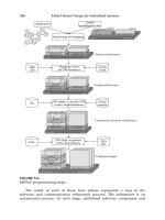
Our optoelectronic modeling is accomplished as shown in Figure 20.1. Given
a device, such as an optical transmitter, we perform linear and nonlinear sub-
block decomposition of the circuit model of the device. This decomposes the
design into a linear multiport subblock section and nonlinear subblocks. The
linear multiport subblock can be thought of as characterizing the intercon-
nection network or parasitics while the nonlinear subblocks characterize the
active devices.
Then, modified nodal analysis (MNA) [26] is used to create a matrix rep-
resentation for the device, as shown in Figure 20.2. In this figure, [S] is the
storage element matrix, [G] is the conductance matrix, [x] is the vector of
state variables, [b] is a connectivity matrix, [u] is the excitation vector, and [I]
is the current vector.
The linear subblock elements can be directly matched to this represen-
tation, but the nonlinear elements need to first undergo a further trans-
formation. We perform piecewise modeling of the active devices for each
nonlinear subblock. When we form each nonlinear subblock, an MNA tem-
plate is used for each device in the network. The use of piecewise models is
based on the ability to change these models for the active devices depending
on the changes in conditions in the circuit, and thus the regions of operation.
The templates generated can be integrated to the general MNA contain-
ing the linear components adding their matrix contents to their correspond-
ing counterparts. This process is shown in Figure 20.2 for the S matrix. This
same composition is done for the other matrices. The size of each of the
Linear
Device
Nonlinear
Piecewise model
Out
In
MNA
template
Modified nodal analysis
MNA composition
Linear solver
(s domain)
g
u
FIGURE 20.1
Piecewise modeling for electrical/optoelectrical devices. (From Kurzweg,
T.P. et al., J. Model. Simul. Micro-Syst., 2, 21, 2001. With permission.)
Nicolescu/Model-Based Design for Embedded Systems 67842_C020 Finals Page 651 2009-10-2
CAD Tools for Multi-Domain Systems on Chips 651
Modified nodal matrix
(S)(x΄) = – (G)(x) + (b)(u); (I) = (b
T
)(x)
(S) Storage element matrix
(S)
Nodes = N
C
L
0
0
C
T
L
T
(G) Conductance matrix
(x) State variables
(b) Connectivity matrix
(u) Excitation vector
(I) Current vector
Template from a
bounded nonlinear
element (i.e., nodes < N
)
(S)
T
FIGURE 20.2
MNA representation and template integration. (From Kurzweg, T.P. et al., J.
Model. Simul. Micro-Syst., 2, 21, 2001. With permission.)
template matrices is bounded by the number of nodes connected to the
nonlinear element.
Once the integrated MNA is formed, a linear analysis in the frequency
domain can be performed to obtain the solution of the system. Constraining
the signals in the system to be piecewise in nature allows us to use a sim-
ple transformation to the time domain without the use of costly numerical
integration.
During each time step in the simulation, the state variables in the mod-
ule will change and might cause the active devices to change their modes
of operation. Therefore, we recompute and recharacterize the PWL solution
caused by changes between piecewise models. Depending on the number of
segments used in the PWL model, on average there will be a large number of
time steps during which the system representation is unchanged, justifying
the computational savings of this technique.
Understanding that the degree of accuracy of PWL models depends
mainly on the step size chosen for the time base, we have incorporated an
adaptive control method for the simulation time step [26]. A binary search
over the time step interval is the basis for this dynamic algorithm. The algo-
rithm discards nonsignificant samples, which do not appreciatively affect the
output, and adds samples when the output change is greater than a user-
defined tolerance. The inclusion of the samples during fast transitions or sup-
pression of time-points during “steady-state” periods optimizes the number
of events used in the simulation.
To support the interaction of electrical models, Chatoyant’s message class
contains parameters that represent general electrical signals that are passed
between electrical devices. Three parameters that are in the message class for
electrical signals are output potential, V, capacitance, C
sb
, and conductance,
g
sb
. The last two fields define the output impedance of the signal, providing
Nicolescu/Model-Based Design for Embedded Systems 67842_C020 Finals Page 652 2009-10-2
652 Model-Based Design for Embedded Systems
a model of loading between electrical devices. We next show an example of
how we use our electrical technique in the modeling of CMOS circuits.
20.2.4.1 Example Modeling of CMOS Circuits
To illustrate our modeling of the active optoelectronic devices in modular
networks, we focus on CMOS driver circuits based on the simple comple-
mentary inverter. Considering the classical nonlinear V–I equations for MOS
transistors (Level II) as characterizing the behavior of every FET device, a
linearization of drain-source current (I
ds
) is presented using
ΔI
ds
= g
m
(P)Δυ
gs
+g
ds
(P)Δυ
ds
(20.1)
where P represents the PWL region of operation for the device. Transcon-
ductance (g
m
) and conductance (g
ds
) are the parameters characterizing the
device. In Figure 20.3a, the parasitic effects (C
ds
, C
gs
,andC
ds
) are introduced.
An MNA template is created from this representation and is shown in Figure
20.3b. This MNA formulation allows us to incorporate the FET as a three-port
element into the MNA of a complete optoelectronic module. The nonlinear
nature of the FET is modeled by piecewise changes in values of the parame-
ters (g
ds
, g
m
, C
ds
, C
gs
,andC
ds
) depending on the region of operation which
are functions of v
g
, v
d
,andv
s
.
To show the speed and accuracy of the PWL approach, we performed sev-
eral experiments comparing our results to that of SPICE 3f4 (Level II). The
test was a multistage amplifier with a significant number of drivers. PWL
models were tested versus SPICE at 10 and 1000 MHz. Figure 20.4 shows
that the speed-up achieved for the same number of time-points is at least
two orders of magnitude compared to SPICE. Accuracy was less than 10%
RMS error. These results show that PWL models are well suited to perform
accurate and fast simulations for the typical multistage CMOS drivers and
transimpedance amplifiers widely used in optoelectronic applications. In the
next section, we show how this same procedure for modeling electronic sig-
nals can be extended for modeling mechanical structures.
20.2.5 Mechanical Models
The general module for solving sets of nonlinear differential equations using
PWL can be used to integrate complex mechanical models in our design tool.
The model for a mechanical device can be summarized in a set of differential
equations that define its dynamics as a reaction to external forces. This model
must then be converted to the form seen in the electrical case to be given to
the PWL solver for evaluation.
In the field of MEM modeling, there has been an increasing amount of
work that uses a set of ordinary differential equations (ODEs) to character-
ize MEM devices [27–29]. ODE modeling is used instead of techniques such
as finite element analysis, to reduce the time and amount of computational
Nicolescu/Model-Based Design for Embedded Systems 67842_C020 Finals Page 653 2009-10-2
CAD Tools for Multi-Domain Systems on Chips 653
(a)
∆v
gs
C
gd
C
db
∆v
ds
∆I
dsn
g
ds
C
gs
g
m
∆v
gs
G
S
D
(b)
*
x
n
+***=–
=
×SG× bu I ×
b
T
g
ds
g
m
g
m
–1
–1
–1
–1
–1
0
0
0
0
0
0
0
00
0
0
0
0
0
00
–1
– g
ds
(– g
ds
–g
m
)
(g
ds
–g
m
)
00 0
0
0
0
00
0
v
d
v
g
v
s
i
d
i
g
i
s
–1
0
0
0
0
0
–1
0
0
0
0
0
–1
0
0
0
0
0
u
d
u
g
u
s
i
D
i
G
i
S
0
0
0
0
0
0
0
0
0
–1
0
0
–1
0
0
–1
0
0
(C
gd
+ C
ds
)
– C
gd
– C
ds
0
0
0
(C
gd
+ C
gs
)
– C
gd
– C
gs
0
0
0
(C
gs
+ C
ds
)
– C
gs
– C
ds
0
0
0
0
0
0
0
0
0
0
0
0
0
0
0
0
0
0
0
0
0
v
d
.
v
g
.
v
s
.
i
d
.
i
g
.
i
s
.
FIGURE 20.3
MOSFET (a) model, (b) template. (From Kurzweg, T.P. et al., J. Model. Simul. Micro-Syst., 2, 21, 2001. With permission.)
Nicolescu/Model-Based Design for Embedded Systems 67842_C020 Finals Page 654 2009-10-2
654 Model-Based Design for Embedded Systems
Spice vs. PWL
1000
100
10
1
Size (# of Fets)
Time (s)
0 50 100 150 200
PWL (10 MHz)
Spice (10 MHz)
Spice (1 GHz)
PWL (1 GHz)
FIGURE 20.4
Spice versus PWL models in a system of multiple FETs.
resources necessary for simulation. The model uses nonlinear differential
equations in multiple degrees of freedom and in mixed domains. The tech-
nique models a MEM device by characterizing its different basic components
such as beams, plate-masses, joints, and electrostatic gaps, and by using local
interactions between components.
Our approach to modeling mechanical elements is to reduce the mechan-
ical ODE representation to a form matching the electronic counterpart, seen
in the equation in Figure 20.2. This enables the use of the PWL technique pre-
viously discussed for simulating the dynamic behavior of electrical systems.
With damping forces proportional to the velocity, the motion equation of
a mechanical structure with viscous damping effects is
F =[K]U +[B]V +[M]A (20.2)
where
[K] is the stiffness matrix
U is the displacement vector
[B] is the damping matrix
V is the velocity vector
[M] is the mass matrix
A is the acceleration vector
F is the vector of external forces affecting the structure
Obviously, knowing that the velocity is the first derivative and the accelera-
tion is the second derivative of the displacement, the above equation can be
recast to
F =[K]U +[B]U
+[M]U
(20.3)
Nicolescu/Model-Based Design for Embedded Systems 67842_C020 Finals Page 655 2009-10-2
CAD Tools for Multi-Domain Systems on Chips 655
Similar to the electrical modeling, this equation represents a set of linear
ODEs if the characteristic matrices [K], [B], and [M] are static and indepen-
dent of the dynamics in the body. If the matrixes are not static and indepen-
dent (e.g., with aerodynamic load effects), they represent a set of nonlinear
ODEs.
To reduce the above equation to a standard form, we use a modification
of Duncan’s reduction technique for vibration analysis in damped struc-
tural systems [30]. This modification allows for the general mechanical
motion equation to be reduced to a standard first order form, similar to
Equation 20.1, which allows for the complete characterization of a mechani-
cal system.
0 M
MB
U
U
+
−M 0
0 K
U
U
=
0
I
F (20.4)
Using substitutions, the equation is rewritten as
[
Mb
]
X
+
[
Mk
]
X =
[
E
]
F (20.5)
where the new state variable vector X =
U
U
.
Each mechanical element (beam, plate, etc.) is characterized by a template
consisting of the set of matrices [Mb]and[Mk], composed of matrices [B],
[M], and [K] in the specified form seen above. If the dimensional displace-
ments are constrained to be small and the shear deformations are ignored,
the derivation of [Mb]and[Mk] is simplified and independent of the state
variables in the system. Additionally, the model for elements is formulated
assuming a one-element idealization (e.g., two nodes for a beam). Conse-
quently, only the static resonant mode is considered. Multiple-element ide-
alization can be performed combining basic elements to characterize higher
order modes.
As an example of our mechanical modeling methodology, we present the
response of an anchored beam in a 2D plane with an external force applied
on the free end. The template for the constrained beam is composed of the
following matrices [31]:
K =
EI
z
l
3
⎡
⎢
⎣
Al
2
I
z
00
012−6l
0 −6l 4l
2
⎤
⎥
⎦
; M =
ρAl
420
⎡
⎣
140 0 0
0 156 −22l
0 −22l 4l
2
⎤
⎦
;
B = δ
⎡
⎣
100
010
000
⎤
⎦
(20.6)
where
E is Young’s modulus
I
z
is the inertia momentum in z
Nicolescu/Model-Based Design for Embedded Systems 67842_C020 Finals Page 656 2009-10-2
656 Model-Based Design for Embedded Systems
A is the area of the beam
l is the length
ρ is the density of the material
δ is the viscosity factor in the system acting over x and y components
The analysis of this element is obtained using the PWL technique pre-
sented above. Constraining the input/output signals to PWL waveforms, the
time domain response is completed in one step, without costly numerical
integration.
To test our results, a comparison against NODAS [28] was performed.
Figure 20.5 shows the frequency response and corresponding resonant fre-
quencies for this constrained beam (183 μm length, 3.8g μm width, poly-Si)
from both our PWL technique and NODAS. The transient response to 1.8
nN nonideal step (rise time of 10 μs) rotational torque is also simulated. The
rotational deformation to this force is shown in Figure 20.6. The compari-
son between our results and those of NODAS are very close. NODAS uses
SABER, a circuit analyzer performing numerical integration for every ana-
lyzed point, which results in costly computation time. Our linear piecewise
solver is computational expensive during the eigenvalue search; however,
this procedure is performed only one time, at the beginning of the simula-
tion run. Overall, this results in a more computationally efficient simulation.
However, as previously mentioned, the accuracy of the analysis depends on
the granularity of the piecewise characterization for the signals used in the
system, which can increase computation time.
Typically, this beam is only a part of a bigger device made from
individual components that are characterized using similar expressions.
NODAS
PWL simulator
150.04 KHz
154.59 KHz 1.52 MHz
1.48 MHz
f
1
f
2
Resonant frequencies
210.0
195.0
180.0
165.0
150.0
135.0
120.0
105.0
f (Hz)
dB(_)
10.0 k 100.0 k 1 meg 10 meg
(a)
210
195
180
165
150
135
120
105
10 k 100 k 1 meg
f (Hz)
10 meg
dB
(b)
FIGURE 20.5
Frequency response of a beam (a) NODAS, (b) Chatoyant.
Nicolescu/Model-Based Design for Embedded Systems 67842_C020 Finals Page 657 2009-10-2
CAD Tools for Multi-Domain Systems on Chips 657
0.3
0.27
0.24
0.21
0.18
0.15
0.12
0.09
0.06
0.03
0
0 10 20 30 40 50 60 70 80 90 100
rad
(b)
(a)
0.3
0.27
0.24
0.21
0.18
0.15
0.12
0.09
0.06
0.03
0.0
0.0
(rad)
10 u 20 u 30 u 40 u 50 u
t(s)
60 u 70 u 80 u 90 u 100 u
FIGURE 20.6
Transient response of a BEAM (a) NODAS, (b) Chatoyant.
The generalization of the previous case to an assembly of elements or
mechanical structure is fairly straightforward. The general expression, seen
in Equation 20.3, characterizes the whole structure defined by a set of nodes,
from which every individual element shares a subset. The next step, simi-
lar to the previously considered electronic case, is merging the individual
templates together, composing the general matrix representation for the
composed structure. However, a common coordinate reference must be used
for this characterization of mechanical structures since every template or ele-
ment is characterized in a local reference system. The process of translation of
these local templates to the global reference system can be described by [31]
[S]=[A]
T
[
¯
S][A] (20.7)
where
[A]represents the translation matrix from local displacements to global dis-
placements (a function of the structure’s geometry)
[
¯
S] represents the local template
[S] is the corresponding global representation
The next step is the addition of these global representations into the general
matrix form, using the matrices’ nodal indexes as reference. Finally, the PWL
solver can be used on the composed system’s general matrix and simulated.
The use of a PWL general solver for mechanical simulation decreases the
computational task and allows for a tradeoff between accuracy and speed.
The additional advantage of using the same technique to characterize elec-
trical and mechanical models allows us to easily merge both technologies in
complex devices that interact in mixed domains.
20.2.6 Optical Propagation Models
Our optical propagation models are based on two techniques: Gaussian
and diffractive scalar. Gaussian models give us fast, accurate results for
macroscale systems and systems that exhibit limited diffraction. Slower
Nicolescu/Model-Based Design for Embedded Systems 67842_C020 Finals Page 658 2009-10-2
658 Model-Based Design for Embedded Systems
diffractive scalar models must be used when diffraction effects dominate the
system.
20.2.6.1 Gaussian Models
Our macroscale optical signal propagation technique is based on Gaussian
beam analysis, allowing paraxial light to be modeled by scalar parame-
ters, and components to be modeled by an optical “ABCD matrix,” which
describes how light is affected by a component [32]. The Gaussian beam is
defined by the nine parameters seen in Table 20.1.
As the parameters in the table indicate, our optical propagation is actually
a mixture of ray analysis and Gaussian analysis. We first find the posi-
tion and direction of the center of the Gaussian beam, using ray propaga-
tion methods. We then “superimpose” the Gaussian beam over this ray to
model its intensity, waist, phase, and depth of focus. The advantage of using
this combination of ray and Gaussian beam analysis is its computational
efficiency. The resulting simulation speed supports interactive system-level
design.
The nine scalar parameters defining the optical signal are represented
in Chatoyant’s message class and passed between components. Each com-
ponent “constructs” an internal model of the beam from these parameters,
alters the beam according to the component function, and then “decom-
poses” the beam back into the propagation parameters, which are returned
to the message class and passed to the next object. The internal model of
the component might simply consist of beam steering, as below, or require
optical power integration, imaging, or optoelectronic conversion.
Using Gaussian beam propagation, components are modeled with the
previously mentioned ABCD matrix. For example, we examine the interac-
tion between a Gaussian beam and a thin lens. To study the beam/lens inter-
action, we start with a definition of the Gaussian beam’s q-parameter, which
characterizes a Gaussian beam of known peak amplitude [32]:
q = z
w0
+jz
0
(20.8)
TABLE 20.1
Gaussian Beam Parameters
Parameter Description
x, y Central position of the Gaussian beam
Rho, theta Directional cosines of the Gaussian beam
Intensity Peak intensity of the Gaussian beam
z
0
Rayleigh range, depth of focus
z
w0
Distance to the next minimum waist
Lambda Wavelength of the light
Phase Phase of the central peak of the beam
Nicolescu/Model-Based Design for Embedded Systems 67842_C020 Finals Page 659 2009-10-2
CAD Tools for Multi-Domain Systems on Chips 659
where the real part is the distance to the minimum waist, and the imaginary
is the Rayleigh range, from which the waist of the beam is determined. The
new Gaussian beam is defined by the following:
q
2
=
Aq
1
+B
Cq
1
+D
(20.9)
where A, B, C, D is the matrix that defines a component. In the case of a thin
lens, A =1,B =0,C =−1/f, D = 1, where f is the focal length of the lens.
Solving for q
2
, and determining the real and imaginary parts, the new z
0
and
zw
0
for the emerging Gaussian beam can be found:
z
0
=
f
2
·z
0
(f −zw
0
)
2
+z
2
0
(20.10)
zw
0
=
f(f · zw
0
−zw
2
0
−z
2
0
)
(f −zw
0
)
2
+z
2
0
(20.11)
The position and direction of the beam is determined from common ray
tracing techniques:
y
2
= Ay
1
+Bθ
1
θ
2
= Cy
1
+Dθ
1
(20.12)
However, as the systems that we wish to design continue to diminish in size,
diffractive effects are a major concern. For example, in optical MEM design,
the size of the components, apertures, and small structures bring diffractive
effects into play, along with the use of diffractive elements such as Fres-
nel zone plates, binary lenses, gratings, and computer generated holograms
(CGH) [33]. Therefore, new design methods are needed that utilize optical
models that can provide accurate diffractive results with reasonable compu-
tational costs. In addition to diffractive effects, other characteristics of opti-
cal signals are important, such as polarization, scattering, phase, frequency
(wavelength) dependence, and dispersion, this last being a requirement for
modeling fiber optic components.
20.2.6.2 Scalar Diffractive Models
To identify which modeling technique is best suited for our needs, we need
to analyze the MDSoCs that we wish to model and evaluate the available
optical propagation techniques. Current optical MEM systems have compo-
nent sizes of roughly tens to hundreds of microns and propagation distances
in the hundreds of microns. With these sizes and distances on the order of
ten to a thousand times the wavelength of light, optical diffractive models
are required.
Figure 20.7 is a description of models of increasing abstraction that begins
at the top with the fundamental vector wave equations, or Maxwell’s equa-
tions, and branches through the different abstraction levels of scalar model-
ing techniques. Along the arrows, notes are added stating the limitations and
approximations that are made for each formulation.
Nicolescu/Model-Based Design for Embedded Systems 67842_C020 Finals Page 660 2009-10-2
660 Model-Based Design for Embedded Systems
Vector wave equations–Maxwell equations
Scalar equations
Rayleigh–Sommerfeld
Fresnel–Kirchoff
Angular spectrum approximation
(near field)
Compute angular spectrum
solve with Fourier transform
Fresnel approximation (near field)
Fraunhofer approximation (far field)
Quadratic phase exponential = 1
solve with Fourier transform
Binomial expansion for the distance from
aperture to observation plane
spherical wave replaced by quadratic
phase exponential (parabolic fronts)
Boundary conditions on field strength
or normal derivative
use for planar components
Diffracting element >> λ
observation plane not close to diffracting element
Boundary conditions on field strength and
normal derivative
use for nonplanar components
FIGURE 20.7
Scalar modeling techniques.
The size and scale of the optical components of MDSoC systems of at least
10 times greater than the wavelength of light lead to the use of scalar diffrac-
tion models. Scalar equations are directly derived from Maxwell’s equations.
Maxwell equations, with the absence of free charge, are [34–36]
∇×
E =−μ
∂
H
∂t
∇×
H =−ε
∂
E
∂t
∇·ε
E = 0 ∇·μ
H = 0 (20.13)
These equations can be recast into the following form:
∇
2
E −
n
2
c
2
∂
2
E
∂t
= 0 ∇
2
H −
n
2
c
2
∂
2
H
∂t
= 0 (20.14)
If we assume that the dielectric medium is linear, isotropic, homogeneous,
and nondispersive, all components in the electric and magnetic field can be