Model-Based Design for Embedded Systems- P29 docx
Bạn đang xem bản rút gọn của tài liệu. Xem và tải ngay bản đầy đủ của tài liệu tại đây (515.26 KB, 10 trang )
Nicolescu/Model-Based Design for Embedded Systems 67842_C009 Finals Page 246 2009-10-13
246 Model-Based Design for Embedded Systems
HDS API
HAL
CPU
Comm.
HALAPI
Task 1 Task 2 Task q
Intra-SubSys comm.
Intra-SubSys comm.
Abstract CPUs
& native SW execution
HdS API
HdS API
Comm. OS
Task 1 Task 2 Task n
Abstract CPUs
& native SW execution
HdS API
HdS API
Comm. OS
Task 1 Task 2 Task n
Abstract intra-
sub system comm.
& native SW execution
HdS API
Task 1 Task 2 Task n
Abstract intra-
sub system comm.
& native SW execution
HdS API
Task 1 Task 2 Task n
Abstract intra-
sub system comm.
Abstract intra-
sub system comm.
Abstract intra-
sub system comm.
Task 1 Task 2 Task n
Abstract intra-
sub system comm.
Task 1 Task 2 Task n
Intra-sub syst comm.
CPU
Peripherals
Intra-sub syst comm.
CPU
Peripherals
Intra-sub syst comm.
Partitioning and mapping
Mapping comm.
on HW resources
SW adapt. to specific HW
comm. implementation
Comm.
implem.
Comm.
archit.
Global
architecture view
SW-SS
HW-SS
Application
HdS
API
OS
SW adapt. to specific
CPUs and memory
CPUs
ISS
HAL
System architecture
Virtual architecture
Transaction accurate architecture
Virtual prototype
Inter-subsystem communication
F
1
F
2
F
3
F
4
F
5
F
8
F
7
F
9
F
10
F
11
Intra-subsyst comm.
Intra-subsyst comm.
CPU
Peripherals
Abstract inter-subsystem communication
Abstract intra-
subsystem comm.
Task 1 Task 2 Task n
Abstract intra-
subsystem comm.
Abstract inter-subsystem communication
Abstract intra-
subsystem comm.
& native SW execution
HdS API
Task 1 Task 2 Task n
Abstract intra-
subsystem comm.
Inter-subsystem communication
Abstract CPUs
& native SW execution
HdS API
HAL API
Comm. OS
Task 1 Task 2 Task n
Intra-subsystem
communication
Inter-subsystem communication
HDS API
HAL
CPU
Comm.
HALAPI
Task 1 Task 2 Task p
HDS API
HAL
CPU Peripherals
Intra-subsyst.comm.
Comm OS
HAL API
Task 1 Task 2 Task n
Intra-subsyst.comm.
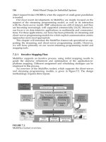
FIGURE 9.6
MPSoC programming steps.
The result of each of these four phases represents a step in the
software and communication refinement process. The refinement is an
incremental process. At each stage, additional software component and
Nicolescu/Model-Based Design for Embedded Systems 67842_C009 Finals Page 247 2009-10-13
Programming Models for MPSoC 247
architecture details are integrated with the previously generated and
validated components. This results to a gradual transformation of a high
level representation with abstract components and high level programming
models into a concrete low level executable software code. The transforma-
tion has to be validated at each design step. The validation can be performed
by formal analysis, simulation, or combining simulation with formal analy-
sis [23]. In the following, we will use simulation-based validation to ensure
that the system behavior respects the initial specification.
During the partitioning and mapping of the application on the target archi-
tecture, the relationship between application and architecture is defined. This
refers to the number of application tasks that can be executed in parallel, the
granularity of these tasks (coarse grain or fine grain), and the association
between tasks and the processors that will execute them.
The result of this step is the decomposition of the application into tasks
and the association between tasks and processors. The resulting model is the
system architecture model. The system architecture model represents a func-
tional description of the application specification, combined with the parti-
tioning and mapping information. Aspects related to the architecture model
(e.g., processing units available in the target hardware platform) are com-
bined into the application model (i.e., multiple tasks executed on the pro-
cessing units). Thus, the system architecture model expresses parallelism in
the target application through capturing the mapping of the functions into
tasks and the tasks into subsystems. It also makes explicit the communication
units to abstract the intra-subsystem communication protocols (the commu-
nication between the tasks inside a subsystem) and the inter-subsystem com-
munication protocols (the communication between different subsystems).
The second step implements the mapping of communication onto the hard-
ware platform resources. At this phase, the different links used for the
communication between the different tasks are mapped on the hardware
resources available in the architecture to implement the specified protocol.
For example, a FIFO communication unit can be mapped to a hardware
queue, a shared memory or some kind of bus-based device. The task code
is adapted to the communication mechanism through the use of adequate
HdS communication primitives. The resulting model is named virtual archi-
tecture model.
The next step of the proposed flow consists of software adaptation to specific
communication protocol implementation. During this stage, aspects related to
the communication protocol are detailed, for example, the synchronization
mechanism between the different processors running in parallel becomes
explicit. The software code has to be adapted to the synchronization method,
such as events or semaphores. This can be done by using the services of OS
and communication components of the software stack. The resulting model
is the Transaction Accurate Architecture model.
The final step corresponds to specific adaptation of the software to the tar-
get processors and specific memory map. This includes the integration of the
Nicolescu/Model-Based Design for Embedded Systems 67842_C009 Finals Page 248 2009-10-13
248 Model-Based Design for Embedded Systems
processor dependent software code into the software stack (HAL) to allow
low level access to the hardware resources and the final memory mapping.
The resulting model is called Virtual Prototype model.
These different steps of the global flow correspond to different software
components generation and validation at different abstraction levels.
9.6 Experiments with H.264 Encoder Application
In this section, we apply the proposed programming environment for a com-
plex MPSoC architecture. The target application corresponds to the H.264
encoder, also called AVC (advanced video coding). Firstly, the specification
of the target architecture and application are given, and then, the program-
ming steps at the system architecture, virtual architecture, transaction accu-
rate architecture, and virtual prototype levels are described, respectively.
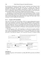
9.6.1 Application and Architecture Specification
The H.264 encoder application is a video processing multimedia applica-
tion that supports coding and decoding of 4:2:0 YUV video formats [24]. The
main functions of the H.264 encoder are illustrated in Figure 9.7. The input
image frame (F
n
) of a video sequence is processed in units of a macroblock,
each consisting of 16 pixels. To encode a macroblock, there are three main
steps: (1) prediction, with the main blocks motion estimation-ME, motion
compensation-MC, and frame filtering; (2) transformation with quantization
(T, Q, and Reorder); and (3) entropy encoding (CABAC in this case). The
H.264 standard supports seven sets of capabilities, which are referred to
T
F
n
ME
Q
Reorder
CABAC
NAL
bitrate control
F
n–1
F
n
Choose
intra pred.
Intra
pred.
Intra
T
–1
Q
–1
MC
Inter
Prediction
.yuv
+
+
+
–
Filter
FIGURE 9.7
H.264 encoder.
Nicolescu/Model-Based Design for Embedded Systems 67842_C009 Finals Page 249 2009-10-13
Programming Models for MPSoC 249
MEM SS ARM9 SS
DXM
NI
SRAM
NI
ARM9
ROM
POT SS
Hermes NoC
NI
Timer
Mailbox
AIC
SPI
NI
DMA
PIC
Mailbox
PMEM
REG1
DMEM1 DSP1
NI
DMA
PIC
Mailbox
PMEM
REG2
DMEM2
DSP2
DSP2 SS
DSP1 SS
FIGURE 9.8
Diopsis R2DT with Hermes NoC.
as profiles, targeting specific class of applications. In this section, the main
profile will be used as an application case study.
The target MPSoC architecture is named Diopsis R2DT (RISC + 2 DSP)
tile [25]. As shown in Figure 9.8, it contains three SW-SS: one ARM9 RISC
processor subsystem and two ATMEL magicV VLIW DSP processing sub-
systems.
The hardware nodes represent the global external memory (DXM) and
POT (peripherals on tile) subsystem. The POT subsystem contains the
peripherals of the ARM9 processor and the I/O peripherals of the tile. All
the three processors may access the local memories and registers of the other
processors and also the distributed external memory (DXM). The different
subsystems are interconnected using the Hermes network on chip (NoC),
which supports two types of topologies: Mesh and Torus [26].
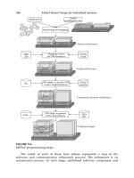
9.6.2 Programming at the System Architecture Level
Programming at the system architecture level consists of functional model-
ing of the application, partitioning the application into the tasks, and map-
ping them onto the processing subsystems.
Therefore, the H.264 application functions are mapped onto the available
SW-SS, as shown in Figure 9.9. Thus, the DSP1-SS is responsible for encoding
a frame of the video sequence. The DSP2-SS compresses the encoded frame.
The ARM9-SS creates the final bitstream and computes the bit-rate controller.
The application executes in pipeline fashion and requires three application
data transfers between the processors: COMM1 between DSP1 and DSP2,
COMM2 between DSP2 and ARM9,andCOMM3 between ARM9 and DSP1.
The resulting system architecture is modeled using the Simulink envi-
ronment. To validate the H.264 encoder algorithm, the system architecture
Nicolescu/Model-Based Design for Embedded Systems 67842_C009 Finals Page 250 2009-10-13
250 Model-Based Design for Embedded Systems
T
T
–1
Q
–1
+
+
+
–
F
n
F
n–1
F
n
Q
Reorder
T1 T2
T3
CABAC
Build NAL
bitrate control
Prediction
Filter
COMM3
COMM1
ARM9-SS
DSP2-SS
DSP1-SS
COMM2
.yuv
FIGURE 9.9
System architecture model of H.264.
model is simulated using a discrete-time simulation engine. The input test
video is a 10 frames video sequence in QCIF YUV 420 format. The simula-
tion requires approximately 30 s on a PC running at 1.73 GHz with 1 GBytes
RAM.
The H.264 simulation allowed validating the functionality, but also mea-
suring early execution requirements. Thus, the total number of iterations nec-
essary to decode the 10 frames video sequence was equal with the number
of frames. This is because of the fact that all the application functions imple-
mented in Simulink operate at the frame level. The communication between
the DSP1 and DSP2 processors uses a communication unit that requires a
buffer of 288,585 words to transmit the encoded frame from the DSP1 pro-
cessor to the DSP2 in order to be compressed. The DSP2 processor and the
ARM9 processor communicate through a communication unit that requires
a buffer of 19,998 words. The last communication unit between the ARM9
and DSP1 processors requires one word buffer size in order to store the
quanta value required for the encoder. The total number of words exchanged
between the different subsystems during the encoding process of the 10
frames video sequence, using main profile configuration of the encoder algo-
rithm, was approximately 3085 kWords.
9.6.3 Programming at the Virtual Architecture Level
Programming at the virtual architecture level consists of generating the C
code for each task from the system architecture model. The generated tasks
code for the H.264 encoder application uses send_data( )/recv_data( )APIs
for the communication primitives and is optimized in terms of data memory
requirements.
Table 9.4 shows the task code and data size of the software at the virtual
architecture level. The first two columns represent the code, respectively the
data size of the functions that are independent of the design and optimiza-
tion methods, which are part of an independent library. The third and fourth
Nicolescu/Model-Based Design for Embedded Systems 67842_C009 Finals Page 251 2009-10-13
Programming Models for MPSoC 251
TABLE 9.4
Task Code Generation for H.264 Encoder
Library Code Library Data Multitasking Code Multitasking Data
Size (Bytes) Size (Bytes) Size (Bytes) Size (Bytes)
270,994 132 366,060 148
DXM
SRAM
T3
T3
T1
T2T1
T2
Abstract ARM9-SS
Comm1
Comm2
Comm3
Abstract DSP2-SSAbstract DSP1-SS
Abstract POT-SS
DMEM1 REG1 DMEM2 REG2
HdS API
HdS API
HdS API
Abstract hermes NoC
FIGURE 9.10
Global view of Diopsis R2DT running H.264.
columns show the code and data size obtained with memory optimization
techniques.
The hardware at the virtual architecture level consists of a SystemC hard-
ware platform, consisting of abstract processor subsystems and interconnect
components. Figure 9.10 illustrates a conceptual view of the virtual architec-
ture for the Diopsis R2DT with Hermes NoC.
The virtual architecture can be simulated not only to validate the tasks
code, but also to gather important early performance measurements to pro-
file the interconnect charge, for instance, the number of words exchanged
between the tasks through the network component or the total packets initi-
ated for the transfer by various subsystems.
Figure 9.11 shows the total words passed through the NoC in case of dif-
ferent communication mapping schemes. Hence, when all the communica-
tion buffers are mapped on the DXM memory, as shown in Figure 9.10, the
NoC is accessed to transfer 6,171,680 words during the encoding process of
the 10 frames. In another case, comm1 is mapped on DXM, comm2 on REG2
and comm3 on DMEM1. This case required 5,971,690 words to be transferred
through the NoC. A third case maps comm1 on DMEM1, comm2 on DMEM2,
and comm3 on SRAM and it generates 3,085,840 words to be operated by
the NoC.
Nicolescu/Model-Based Design for Embedded Systems 67842_C009 Finals Page 252 2009-10-13
252 Model-Based Design for Embedded Systems
Total words
DXM + SRAM + DXM
DMEM1 + SRAM + DXM
DXM + DXM + REG1
DMEM2 + DXM + SRAM
DMEM1 + DMEM2 + SRAM
DXM + DMEM2 + DMEM1
DXM + DXM + DXM
0 1,000,000 2,000,000 3,000,000 4,000,000 5,000,000 6,000,000 7,000,000
5,971,700
3,085,850
6,171,670
3,285,820
3,085,840
5,971,690
6,171,680
FIGURE 9.11
Words transferred through the Hermes NoC.
TABLE 9.5
Results Captured in Hermes NoC Using DXM as Communication
Scheme
Read/Write Total Sent
H.264 NoC Address Requests Packets Sent MBytes
DXM 0 ×0 0 83,352 17,324
ARM9-SS 1 ×0 2,426 4,853 68
DSP1-SS 1 ×1 39,260 78,522 16,167
DSP2-SS 1 ×2 41,663 83,327 2,090
Table 9.5 summarizes the results captured during the simulation of the
H.264 encoder application in case of the first communication scheme, with all
the buffers mapped on the DXM memory. The first and the second columns
represent the correspondence between the different cores connected to the
NoC and the NoC addresses. The third column represents the total num-
ber of reads and writes requested over the NoC. Based on these values, the
designer may define a better mapping of hardware cores over the NoC or
the size of packets. The fourth and the fifth columns (Packets and MBytes
sent) allow evaluating the real amount of communication injected into the
NoC through each network interface. In this example, the DXM was the core
that inserted the biggest amount of data in the NoC. The DXM packets are
originated from read requests and confirmation packets.
In all the communication mapping schemes, the simulation time required
to encode the 10 image frames using QCIF YUV 420 format was approxi-
mately 40 s on a PC running Linux OS at 1.73 GHz.
Nicolescu/Model-Based Design for Embedded Systems 67842_C009 Finals Page 253 2009-10-13
Programming Models for MPSoC 253
9.6.4 Programming at the Transaction Accurate
Architecture Level
Programming at the transaction accurate architecture level means to build
each software stack running on the processors. This consists of combining
the tasks code with the OS and communication libraries. Thus, the H.264
tasks code previously designed is combined with a tiny OS necessary for the
interrupts management and the tasks initialization, and the implementation
of the send_data( )/recv_data( )communication primitives. The processors
execute single task on top of the OS.
The transaction accurate architecture of the Diopsis R2DT tile with Her-
mes NoC is illustrated in Figure 9.12. The hardware platform is composed
of the three processor subsystems (ARM9-SS, DSP1-SS, and DSP2-SS), one
global MEM-SS, and the peripherals on tile subsystem (POT-SS), all sub-
systems having the local architecture detailed. The different subsystems are
interconnected through an explicit Hermes NoC.
The simulation of the transaction accurate architecture allows validating
the integration of the tasks code with the OS and communication libraries,
but it also provides better performance estimation, such as communication
performances.
At this level, in order to analyze the overall system performance, we
experimented with several communication architectures by changing the
interconnection component and/or communication mapping scheme. The
NoC allows various mapping schemes of the IPs over the NoC with different
impact on performance. In this work, two different mappings of the IP cores
MEM-SS
DXM
NI
SRAM
ARM9-SS
NI
Abstract
ARM9
Hermes noc
POT-SS DSP1-SS DSP2-SS
NI
Timer
Mailbox
Mailbox
Mailbox
AIC SPI
NI
DMA
PIC
REG1
DMEM1
Abstract
DSP1
NI
DMA
PIC
REG2
DMEM2
Abstract
DSP2
HdS API
Comm
OS
HAL API
HdS API
Comm
OS
HAL API
HdS API
Comm
OS
HAL API
T1
T3
T2
SW Stack DSP1
SW Stack ARM9
SW Stack DSP2
FIGURE 9.12
Global view of the transaction accurate architecture for Diopsis R2DT with
Hermes NoC running H.264 encoder application.
Nicolescu/Model-Based Design for Embedded Systems 67842_C009 Finals Page 254 2009-10-13
254 Model-Based Design for Embedded Systems
Y\ X 0 1 2
0 MEM-SS POT-SS -
1 ARM9-SS DMA1 DMA2
2 - DSP1-SS DSP2-SS
Scheme A
Y\X 0 1 2
0 DMA1 - -
1 ARM9-SS MEM-SS DSP2-SS
2 POT-SS DSP1-SS DMA2
Scheme B
FIGURE 9.13
IP cores mapping schemes A and B over the NoC.
over the Mesh and Torus NoC are experimented: Scheme A and Scheme B,
respectively. Figure 9.13 summarizes these schemes by presenting the corre-
spondence between the Network Interface and the IP core, e.g., the MEM-SS
is connected in Scheme B at the network interface with address 1 × 1(bothx
and y coordinates are 1).
Table 9.6 presents the results of the transaction accurate simulations
for various interconnection components (AMBA bus, NoC) with different
topologies for the NoC (Torus, Mesh), different IP cores mapping over the
NoC and diverse communication buffer mapping schemes. The estimated
performance indicators are: estimated execution cycles of the H.264 encoder,
the simulation time using the different interconnect components on a PC
running at 1.73 GHz with 1 GBytes RAM and the total routing requests
for the NoC. These results were evaluated for the two considered IP map-
ping schemes shown in Figure 9.13 (A and B) and for three communication
buffer mapping schemes: DXM+DXM+DXM, DMEM1+DMEM2+SRAM
and DMEM1+SRAM+DXM. The AMBA had the best performance, as it
implied the fewest clock cycles during the execution for all the communi-
cation mapping schemes. The Mesh NoC attained the worse performance in
case of mapping all the communication buffers onto the DXM and similar
performance with the Torus in case of using the local memories.
This is explained by the small numbers of subsystems interconnected
through the NoC. In fact, NoCs are very efficient in architectures with
more than 10 IP cores interconnected, while they can have a compara-
ble performance results with the AMBA bus in less complex architectures.
Between the NoCs, the Torus has better path diversity than the Mesh. Thus,
Torus reduces network congestion and decreases the routing requests. Also,
Scheme A of IP cores mapping provided better results than Scheme B for the
DMEM1+DMEM2+SRAM buffer mapping. For the other buffer mappings
the performance of Scheme A was superior to Scheme B. In fact, the ideal
IP cores mapping scheme would have the communicating IPs separated by
only one hop (number of intermediate routers) over the network to reduce
latency.
9.6.5 Programming at the Virtual Prototype Level
Programming at the virtual prototype level consists of integrating the HAL
layer into the software stack for each particular processor subsystem and to
Nicolescu/Model-Based Design for Embedded Systems 67842_C009 Finals Page 255 2009-10-13
Programming Models for MPSoC 255
TABLE 9.6
Execution and Simulation Times of the H.264 Encoder for Different Interconnect, Communication, and IP Mappings
Execution Average
Communication IPs Time at Simulation NoC Interconnect
Mapping Mapping 100 MHz Simulation Execution Cycles/ Routing Latency
Scheme Interconnect over NoC (ns) Time (min) Cycles Second Requests (Cycles/Word)
DXM + DXM + DXM Mesh Scheme A 64,028,725 36 min 3,201,436 1482 96,618,508 25
DXM + DXM + DXM Torus Scheme A 46,713,986 28 min 29 s 2,335,699 1527 78,217,542 16
DMEM1 + DMEM2
+SRAM
Mesh Scheme A 28,573,705 12 min 54 s 1,428,685 1846 13,118,044 10
DMEM1 + DMEM2
+SRAM
Torus Scheme A 26,193,039 12 min 1,309,652 1819 12,674,692 9
DMEM1 + SRAM +
DXM
Mesh Scheme A 26,233,039 14 min 55 s 1,594,237 1466 13,144,538 11
DMEM1 + SRAM +
DXM
Torus Scheme A 26,193,040 14 min 48 s 1,309,652 1475 14,479,723 10
DXM + DXM + DXM Mesh Scheme B 35,070,577 18 min 34 s 1,753,529 1574 24,753,610 9
DXM + DXM + DXM Torus Scheme B 35,070,587 19 min 8 s 1,753,529 1527 24,753,488 9
DMEM1 + DMEM2
+SRAM
Mesh Scheme B 31,964,760 17 min 8 s 1,598,238 1555 18,467,386 13
DMEM1 + DMEM2
+SRAM
Torus Scheme B 31,924,752 16 min 14 s 1,595,238 1639 15,213,557 13
DMEM1 + SRAM +
DXM
Mesh Scheme B 31,964,731 18 min 38 s 1,598,237 1430 18,512,403 15
DMEM1 + SRAM +
DXM
Torus Scheme B 31,924,750 16 min 42 s 1,596,238 1593 18,115,966 14
DXM + DXM + DXM AMBA — 17,436,640 8 min 24 s 871,832 1730 — 9
DMEM1 + DMEM2
+SRAM
AMBA — 17,435,445 7 min 18 s 871,772 1990 — 9
DMEM1 + SRAM +
DXM
AMBA — 17,435,476 7 min 17 s 871,774 1995 — 9